Note: Descriptions are shown in the official language in which they were submitted.
CA 02460988 2004-03-18
WO 03/026236 PCT/CA02/01419
Transmit Amplitude Independent Adaptive Equalizer
BACKGROUND
1. FIELD OF THE INVENTION
This invention relates generally to the field of equalizers. More
particularly, the
invention provides a transmit amplitude independent adaptive equalizer that is
capable of
compensating for transmission losses in an input signal when the transmit
signal amplitude is
unknown. The invention is particularly well suited for use in digital
communication
components, such as receivers, equalizers, high-speed backplanes, Printed
Circuit Board Trace
equalizers, automatic gain control devices, and other types of digital
communication
components.
2. DESCRIPTION OF THE RELATED ART
The use of an equalizer to compensate for loss resulting from the non-
idealities of a
transmission medium is known. Fig. 1 is a block diagram showing an equalizer
12 implemented
in a typical digital communications system 10 in which an input signal 14 is
transmitted through
a transmission medium 16. Typical transmission media 16 used for transmission
of digital
signals over relatively short distances include, for example, printed circuit
board (PCB) traces
and coaxial cables. These, and other known transmission media, typically cause
significant
frequency dependant losses in digital signals being transmitted over the media
and consequently
distort the digital data, often resulting in pulse spreading and interference
between neighboring
pulses (known as intersymbol interference). In addition, the input signal 14
is further corrupted
during transmission by noise 1 ~ induced by the transmission medium 16. The
equalizer 12
regenerates the transmitted signal 20 by providing gain to compensate for the
frequency
1
CA 02460988 2004-03-18
WO 03/026236 PCT/CA02/01419
dependant losses caused by the transmission medium 16 (up to some maximum
length) while
preferably minimizing the effect of noise 18. This function is typically
achieved by applying a
transfer function to the received signal 20 that approximates the inverse of
the transmission
losses.
Fig. 2 is a graph 30 showing the loss (in dB) incurred in the transmission
medium 16,
plotted as a function of both the length (1) of the medium 16 and the
frequency ( f ) of the
signal. Generally, the loss over a transmission medium (such as a coaxial
cable or PCB trace)
may be approximated in the frequency domain by the following equation:
L( f) = a 'c~'~+~III~ .
where f is the frequency, 1 is the length of the transmission medium, j = ~ ,
ks is the skin
effect loss constant of the transmission medium, and ka is the dielectric loss
constant of the
transmission medium. The value of L( f ) is plotted in Fig. 2 for transmission
media of two
different lengths: Length 1'(shorter) and Length 2 (longer). As the length (l)
of the transmission
medium increases, the loss increases. In addition, as the frequency ( f )
increases, the loss
increases.
To counteract the transmission loss shown in Fig. 2, an equalizer 12 should
have a
frequency characteristic that is the inverse of the loss function of the
transmission medium. The
inverse loss function may be approximated as follows:
1 =G(f)=1+KH(f);
L(f)
where K is a control variable that is proportional to the length (l) of the
transmission medium.
The value of K typically varies from zero to unity (or some other constant) as
the transmission
medium approaches its maximum length.
2
CA 02460988 2004-03-18
WO 03/026236 PCT/CA02/01419
Fig. 3 is a graph 40 showing the inverse loss function G( f ) , plotted in dB
on the same
axes as the loss function L( f ). As shown in this figure, the inverse loss
function G( f ) provides
a frequency dependant gain equivalent to the loss L( f ) incurred in the
transmission medium.
The characteristics of the inverse loss function G( f ) are explained in more
detail in United
r
States Patent Application No. 09/055,5 1 S .(hereinafter referred to as "the
'S 1 S Application")
which is owned by the Assignee of the present application, and which is hereby
incorporated into
the present application by reference.
Fig. 4 is a block diagram of an equalizer core SO that implements the inverse
loss
function G( f ) . The equalizer core SO includes a transfer function block S2
( H( f ) ), a multiplier
S8, and an adder S6. This circuit SO applies variable gain to an input signal
S7 by applying the
transfer function H( f ) in order to generate a resultant signal and then by
multiplying the
resultant signal from the transfer function block S2 by a gain control signal
S8 (K). The gain
control signal S8 (K) preferably controls the amount of gain applied by the
transfer function
H( f ) by multiplying the output of the transfer function block S2 by a factor
typically varying
from zero (0) to unity (1) depending upon the length (l) of the transmission
medium 16. For
instance, when the transmission medium I6 is at a maximum length, the transfer
function H( f
is generally multiplied by unity (1) to provide the maximum gain. The output
of the multiplier is
then summed with the input signal S7 by the adder S6 in order to produce an
equalized output
signal S9 corresponding to the inverse loss function (1+ KH(f)). An exemplary
circuit for
implementing the transfer function block S2 is described in the above-
referenced 'S 15
Application.
Fig. S is a block diagram of an alternative equalizer core 60 that implements
a bandwidth-
limited inverse loss function. In this circuit 60, a low-pass filter 62 is
added to the equalizer core
3
CA 02460988 2004-03-18
WO 03/026236 PCT/CA02/01419
50 shown in Fig. 4 to reduce noise encountered in the transmission medium 16.
This alternative
implementation 60 reduces the amplification of high frequency noise, and thus
increases the
signal-to-noise ratio (SNR) of the equalized output signal 64. A graphical
representation 70 of
the bandwidth-limited inverse loss function 72, plotted on the same axes as
the Ioss function
L( f ) is shown in Fig. 6.
Fig. 7 is a block diagram showing a multiple-stage equalizer core 80 having
three
equalizer stages 82, 84 and 86, each of which implements the inverse loss
function G( f ) . The
three cascaded equalizer stages 82, 84 and 86 are preferably the same as the
equalizer core 50
shown in Fig. 4. Alternatively, the multiple-stage equalizer core 80 could
include a plurality of
bandwidth-limited stages as shown in Fig. 5, or other types of cores. In any
case, each equalizer
stage 82, 84 and 86 includes a gain control signal (K1, K2 or K3) that is used
to control the gain
implemented by the transfer function H( f ) in proportion to the length of the
transmission
medium 16. The advantages of utilizing a multiple-stage equalizer core are
explained in detail in
the '515 Application.
Operationally, each stage 82, 84 and 86 in the multiple-stage equalizer core
80 is
configured to equalize signals transmitted over transmission media up to a
percentage of the total
maximum transmission medium length. For instance, if the multiple-stage
equalizer .core 80 is
capable of equalizing losses incurred in a printed circuit board ("PCB") trace
of up to 30 inches,
then each core stage 82, 84, and 86 will typically be configured to equalize
losses in PCB traces
of up to 10 inches. The stages 82, 84 and 86 are then cascaded such that they
operate
sequentially to equalize PCB traces of up to 30 inches.
Fig. 8 is a graph 90 showing how the gain control signals Kl, K2 and K3 in the
multiple-
stage equalizer core 80 are varied according to the length of the transmission
medium. The value
4
CA 02460988 2004-03-18
WO 03/026236 PCT/CA02/01419
K, shown along the x-axis in Fig. 8, represents the percentage of the transfer
function H( f ) that
needs to be applied to an input signal in order to supply the gain necessary
to equalize a
transmission medium of a given length. As the transmission medium length
increases, the gain
necessary to equalize the transmission losses in the medium also increases.
Fig. 8 shows that
the gain control signals Kl, K2 and K3 cause gain to be supplied sequentially
by the equalizer
stages 82, 84 and 86. For instance, if each equalizer stage 82, 84 and 86 is
capable of providing
the necessary gain to equalize 10 inches of a PCB trace, then the gain control
signal Kl would
typically control the gain necessary for PCB traces from 0 to 10 inches, the
combined gain
control signals Kl (at unity) and K2 would typically control the gain
necessary for PCB traces
from 10 to 20 inches, and the combined gain control signals Kl (at unity), K2
(at unity) and K3
would typically provide the gain for PCB traces from 20 to 30 inches. For
example, if the PCB
trace were 15 inches in length and each equalizer stage 82, 84 and 86 can
equalize 10 inches,
then Kl would be at its maximum value (unity), K2 would be at the value
necessary tv cause the
second equalizer stage 84 to equalize a 5 inch transmission medium, and K3
would be zero.
Fig. 9 is a block diagram showing an exemplary equalizer system 100 such as
described
in the referenced 'S 15 Application. This equalizer system 100 includes an
equalizer core 102, a
slicer 104, an automatic gain control circuit (AGC) 106, a transmitter 108,
and a transmission
medium 110. The equalizer core 102 may be either a single-stage core as shown
in Figs. 4 or 5
or a multiple-stage core as shown in Fig. 7, and operates, as described above,
to compensate for
the losses incurred in the transmission medium 110. The output 112 of the
equalizer core 102 is
coupled to the slicer 104, which converts the output signal 112 from the core
102 to a digital
output signal 114 having a known swing (A) that.approximates the swing (B) of
the data sent
from the transmitter 108. Since the swing (B) of the transmitted data is known
and reproduced
CA 02460988 2004-03-18
WO 03/026236 PCT/CA02/01419
as the swing (A) of the digital output signal 114 from the dicer 104, the
difference in energy
between the equalizer core output signal 112 and the digital output signal 114
approximates the
energy lost in the transmission medium 110, which is proportional to its
length. The AGC I06
compares the energy of the equalizer core output signal 112 with the energy of
the digital output
signal 114 from the dicer 104 to generate the gain control signal K.
The AGC 106 includes a core-side band-pass filter 116, a core-side envelope
detector
I18, a slicer-side band-pass filter 120, a slicer-side envelope detector 122,
an adder 124, and a
sequences 126. Operationally, the AGC 106 filters the core and digital outputs
112 and I I4 to
mid-band frequencies using the band-pass filters 116 and 120. The advantage of
filtering the
core and digital outputs 112 and I I4 to their mid-band frequencies is
explained in detail in the
'S 1 S Application. Following this filtering function, the AGC I 06 then
detects the signal energy
of the two band-limited signals with the envelope detectors 118 and 122.
Finally, it determines
the difference between the two signal energies with the adder 124, which
provides the gain
control signal K. If the equalizer core I02 is single-stage, then the gain
control signal K is
typically coupled directly to the core 102 to control the variable gain as
described above. If,
however, the equalizer core i02 is of the multiple-stage type, then the
sequences 126 is used to
convert the gain control signal K from the adder 124 into a plurality of
multiple-stage gain
control signals Ki, such as Kl, K2 and K3 described above with reference to
Figs. 7 and 8. In
either case, the gain control signals) K (or Ki) enable the equalizer core 102
to equalize the core
output signal 112 by forcing it to the same energy level as the digital output
signal 114 from the
slices 104. A further description of the AGC 106 is provided in the above
referenced 'S1S
Application.
6
CA 02460988 2004-03-18
WO 03/026236 PCT/CA02/01419
One skilled in the art will appreciate that the signal swing (B) at the
transmitter 108 must
be known a priori and accurately replicated by the slicer 104 if the equalizer
system 100 shown
in Fig. 9 is to achieve optimal performance. Any significant difference
between the signal swing
(B) at the transmitter 108 and the signal swing (A) of the digital output
signal 114 will directly
result in a gain (equalization) error. For example, an increase in the swing
(B) of the transmitted
signal will force the AGC loop 106 to settle at a lower gain than necessary to
compensate for the
transmission loss (under-equalization). Similarly, a decrease in the swing (B)
of the transmitted
signal will result in over-equalization. Even if the swing (B) of the
transmitted signal were
tightly controlled, similar equalization errors may be caused by mismatch in
the digital output
swing (A) generated by the slicer 104. Such mismatch errors may be caused, for
example, by
variations in temperature, power supply voltages, or manufacturing processes.
SUMMARY
A transmit amplitude independent adaptive equalizer is provided. One
embodiment of
the equalizer comprises an equalizer core, a controllable-swing slicer and an
amplitude control
loop. The equalizer core is coupled to an input signal from a transmission
medium, and
generates a core output signal by applying a frequency dependant gain to the
input signal to
compensate for losses incurred in the transmission medium. The controllable-
swing slicer is
coupled to the core output signal and a swing control input, and converts the
core output signal
into a digital output signal having a variable swing that is controlled by the
swing control input.
The amplitude control loop is coupled to the core output signal and the
digital output signal, and
generates the swing control input by comparing the core output signal with the
digital output
signal.
7
CA 02460988 2004-03-18
WO 03/026236 PCT/CA02/01419
A second embodiment of the equalizer comprises an equalizer core, a fixed-
swing dicer,
and a control loop. The equalizer core is coupled to an input signal from a
transmission medium
and a gain control input, and generates a core output signal by applying a
frequency dependant
gain to the input signal. The frequency dependant gain is controlled by the
gain control input
and compensates for losses incurred in the transmission medium. The fixed-
swing slicer is
coupled to the core output signal and converts the core output signal to a
digital output signal
having a fixed digital output swing. The control Ioop is coupled to the core
output signal and the
digital output signal and normalizes the core and digital output signals with
respect to their low-
frequency energy levels, compares the normalized core output signal with the
normalized digital
output signal to approximate a normalized energy level difference, and
generates the gain control
input.
A third embodiment of the equalizer comprises a variable gain amplifier, a
variable gain
amplifier control loop, and an equalizer core. The variable gain amplifier is
coupled to an input
signal from a transmission,medium and a variable ain control si
g gnat, and applies a variable gain
to the input signal to generate an equalizer core input signal having a pre-
determined signal
swing. The variable gain amplifier control loop is coupled to the input signal
and the equalizer
core input signal, and compares the input signal with the equalizer core input
signal in order to
generate the variable gain control signal. The equalizer core is coupled to
the equalizer core
input signal, and applies a frequency dependant gain to the amplifier output
in order to
compensate for attenuation of the input signal caused by losses incurred in
the transmission
medium.
A fourth embodiment of the equalizer corr~prises a variable gain amplifier, an
equalizer
core, a fixed-swing slicer and a variable gain amplifier control loop. The
variable gain amplifier
8
CA 02460988 2004-03-18
WO 03/026236 PCT/CA02/01419
is coupled to an input signal from a transmission medium and is also coupled
to a variable gain
control signal. The variable gain amplifier applies a variable gain to the
input signal in order to
generate an equalizer core input signal having a pre-determined signal swing.
The equalizer core
is coupled to the equalizer core input signal, and applies a frequency
dependant gain to the
amplifier output in order to compensate for attenuation of the input signal
that is caused by losses
incurred in the transmission medium and generates a core output signal. The
fixed-swing slicer
is coupled to the core output signal, and converts the core output signal into
a digital output
signal having the pre-determined signal swing. The variable gain amplifier
control loop is
coupled to the core output signal and the digital output signal, and compares
the core output
signal with the digital output signal in order to generate the variable gain
control signal.
BRIEF DESCRIPTION OF THE DRAWINGS
Fig. 1 is a block diagram showing the use of an equalizer in a typical serial
digital data
communication system in which an input signal is transmitted through a
transmission medium;
Fig. 2 is a graph showing the loss (in dB) incurred in the transmission
medium, plotted as
a function of both the length (l) of the medium and the frequency ( f ) of the
signal;
Fig. 3 is a graph showing the inverse loss function G( f ) plotted on the same
axes as the
loss function L( f ) ;
Fig. 4 is a block diagram of an equalizer core that implements the inverse
loss function
G(f )
Fig. 5 is a block diagram of an alternative equalizer core that implements a
bandwidth-
limited inverse loss function;
9
CA 02460988 2004-03-18
WO 03/026236 PCT/CA02/01419
Fig. 6 is a graphical representation of the bandwidth-limited inverse loss
function, plotted
on the same axes as the loss function L( f ) ;
Fig. 7 is a block diagram showing a known multiple-stage equalizer core in
which each
stage implements the inverse loss function G( f ) ;
Fig,. 8 is a graph showing how the gain control signals in the multiple-stage
equalizer core
are adjusted according to the length of the transmission medium;
Fig. 9 is a block diagram showing an exemplary equalizer system such as
described in the
referenced 'S I S Application;
Fig. I0 is a block diagram of an exemplary transmit amplitude independent
adaptive
equalizer having a controllable-swing slicer according to one embodiment of
the claimed
invention;
Fig. 11 is a block diagram of an exemplary transmit amplitude independent
adaptive
equalizer having a fixed-swing slicer according to another embodiment of the
claimed invention;
Fig. 12 is a block diagram of a transmit amplitude leveling circuit for an
equalizer;
Fig. 13 is a block diagram illustrating an exemplary implementation of the
received data
swing detection circuit and the core input swing detection circuit shown in
Fig. 12; and
Fig. 14 is a block diagram of an exemplary transmit amplitude independent
adaptive
equalizer utilizing a variable gain amplifier.
DETAILED DESCRIPTION
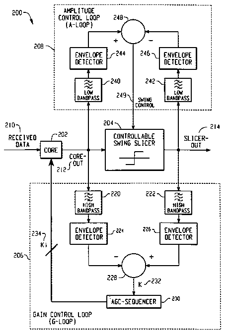
Referring again to the drawing figures, Fig. 10 is a block diagram of an
exemplary
transmit amplitude independent adaptive equalized 200 having a controllable-
swing slicer 204.
The equalizer 200 includes an equalizer core 202, a controllable-swing slicer
204, a gain control
CA 02460988 2004-03-18
WO 03/026236 PCT/CA02/01419
loop (G-Loop) 206, and an amplitude control loop (A-Loop) 208. The G-Loop 206
includes two
high band-pass filters 220 and 222, two envelope detectors 224 and 226, an
adder 228, and a
sequencer 230. The amplitude control loop (A-Loop) 208 includes two low band-
pass filters 240
and 242, two envelope detectors 244 and 246, and an adder 248.
Operationally, the amplitude independent adaptive equalizer 200 tracks the
amplitude at
which its input signal 210 was transmitted by varying the swing of its digital
output signal 214 to
approximate the swing of the transmitted data. Because the loss incurred in a
transmission
medium is frequency dependant, the low frequency portion of the equalizer's
input signal 210
shows substantially less attenuation than the higher frequency portions. The
equalizer 200 thus
detects the amplitude of its input signal 2I0 at a low frequency, and uses
this low-frequency
amplitude to approximate the swing of the transmitted data.
The equalizer core 202 receives the input signal 210 from a transmission
medium ,and
generates a core output signal 212. The input signal 210 is preferably a
digital signal that has
been attenuated during . transmission over a transmission medium. The
equalizer core 202
compensates for attenuation and distortion in the input signal 210 by applying
an inverse loss
function G( f ) as described above with reference to Figs. 2-8. The equalizer
core 202 also
receives a gain control signal (Ki) 234 from the gain control loop (G-Loop)
206, which controls
the gain applied by the inverse loss function G( f ) . The core output signal
212 is then coupled
to the controllable-swing slicer 204, which converts the core output signal
212 into a digital
output signal 214 having a swing that is controlled by the amplitude control
loop (A-Loop) 208.
The A-Loop 208 isolates the low frequency portions of the core output signal
212 and the digital
output signal 214, and compares the signal energies of the two low band-
limited signals to set the
controllable-swing slicer 204 to approximate the swing of the equalizer input
210 prior to
11
CA 02460988 2004-03-18
WO 03/026236 PCT/CA02/01419
transmission. Similarly, the high frequency portions of the core output signal
212 and the digital
output signal 214 are isolated by the gain control loop (G-Loop) 206, which
compares the signal
energies of the high band-limited signals to generate the gain control signal
(Ki) 226. Preferably,
the low band-limited signals are centered towards the low end of the transmit
spectrum at which
the transmission losses are minimal, and the high band-limited signals are
centered towards the
higher end of the transmit spectrum at which the transmission losses are more
significant.
However, the low and high band-limited signals may be centered at alternative
points within the
transmit spectrum as long as the A-Loop 208 isolates a lower spectral range
than the G-Loop
206.
Within the A-Loop 208, the low frequency portions of the core output signal
212 and the
digital output signal 214 are isolated by the low band-pass filters 240 and
242. The low band-
limited signals are each coupled to one of the envelope detectors 244 and 246,
which detect the
signal energies. The envelope detectors 244 and 246 may preferably be
comprised of rectifiers,
but could alternatively be any device or combination of devices capable of
generating an output
signal proportional to the signal energy of its input. The difference between
the energy-level
outputs from the envelope detectors 244 and 246 is then determined by the
adder 248.
Preferably, the energy difference is calculated by coupling the energy-level
output from one
envelope detector 244 as a positive input to the adder 248, and the energy-
level output from the
other envelope detector 246 as a negative input to the adder 248. In this
manner, the adder 248
generates a swing control signal 249 that is proportional to the energy
difference between the
low band-limited signals. The swing control signal 249 is coupled to the
controllable-swing
dicer 204 to control the energy level of the digital output signal 214.
Operationally, the A-Loop
swing control signal 250 forces the swing of the digital output 214 to match
the swing of the low
12
CA 02460988 2004-03-18
WO 03/026236 PCT/CA02/01419
band-limited core output. Because the low band-limited core output is
typically not significantly
attenuated by the transmission medium, the swing of the digital output 214 is
thus made to
approximate the swing of the equalizer input 210 prior to transmission.
Within the G-Loop 206, the higher frequency portions of the core output signal
2I2 and
the digital output signal 2I4 are isolated by the high band-pass filters 220
and 222, The
bandwidths of the high band-pass filters 220 and 222 are preferably set to
isolate the frequency
band in which the equalizer input signal 210 is most significantly effected by
transmission
losses. Once the core and digital outputs 212 and 214 have been band-limited
by the high band-
pass filters 220 and 222, the signals are respectively coupled to the input of
the envelope
detectors 224 and 226, each of which generates an energy-level output
proportional to the signal
energy of its input signal. The difference between the energy-Ievel outputs of
the envelope
detectors 224 and 226 is preferably determined by coupling one energy-level
output as a negative
input to the adder 228 and coupling the other energy-level output as a
positive input to the adder
228. The adder 216. then generates a single-stage gain control signal (K) 232
that is proportional
to the energy difference between the band-limited core and digital output
signals. Because this
energy difference approximates the energy lost during transmission over the
transmission
medium, the single-stage gain control signal (K) 232 settles to a value
proportional to the
transmission loss which is a function of the length of the transmission
medium. The single-stage
gain control signal (K) 232 is coupled to the sequences 230, which generates
the gain control
signal Ki 234 that is fed back to control the gain of the equalizer core 202
as described above
with reference to Figs. 7 and 8. Alternatively, if the equalizer core 202 is a
single-stage equalizer
core as described above with reference to Fig. 4 or Fig. 5, then the single-
stage gain control
signal (K) 232 may be directly fed back to the equalizer core 202.
13
CA 02460988 2004-03-18
WO 03/026236 PCT/CA02/01419
It should be understood that many types of controllers could be used to
implement the A-
Loop 208 and the G-Loop 206 shown in Fig. 10. For instance, the A-Loop 208 and
the G-Loop
206 may be implemented as either a proportional type controller (P-Type), an
integral type
controller (I-Type) or a combination PI-type controller. To implement the G-
Loop 206 as an I-
Type controller, for example, an integrator (I~1/s) could be coupled between
the adder 228 and
the sequencer 230. In addition, to maintain stability in the system, the A-
Loop 208 and the G-
Loop 206 are preferably implemented as different controller types such that
one control loop 206
or 208 has a dominant time constant/pole. For example, the G-Loop 206 may
preferably be
implemented as a slower I-type loop, while the A-Loop 208 is implemented as a
faster P-Type
loop.
Fig. 11 is a block diagram of an exemplary transmit amplitude independent
adaptive
equalizer 300 having a fixed-swing slicer 304. In this exemplary embodiment,
the amplitude
independent adaptive equalizer 300 includes an equalizer core 302, a slicer
304, and a control
loop 305. The control loop includes a core-side low band-pass filter 306, a
core-side high band-
pass filter 308, a slicer-side low band-pass filter 310, a slicer-side high
band-pass filter 312, four
envelope detectors 314, 316, 318 and 320, a core-side multiplier 340, a dicer-
side multiplier 342,
an adder 322, and a sequencer 324. Operationally, the equalizer 300 utilizes a
fixed-swing slicer
304, which is independent from the amplitude of the equalizer's input signal
332. To accomplish
amplitude independence and maintain optimal equalization, the equalizer 300
calculates the
necessary gain by first normalizing the energy Level at the outputs of the
equalizer core 302 and
the fixed-swing slicer 304 with respect to their Low-frequency amplitudes, and
then comparing
the normalized signals.
14
CA 02460988 2004-03-18
WO 03/026236 PCT/CA02/01419
The equalizer core 302 receives an input signal 332 from a transmission medium
and a
gain control signal (Ki) 303 from the control loop 305. As described above,
the equalizer core
302 applies a frequency dependant gain to the equalizer input signal 332 as a
function of the gain
control signal (Ki), and generates a core output signal 326. The core output
signal 326 is then
coupled to the fixed-swing slicer 304, which converts the core output signal
326 into a digital
output signal 328 having a fixed swing. Preferably, the swing (A) of the
digital output signal is
fixed at a nominal value at which data is most often transmitted to the
equalizer 300. Because
the equalizer 300 is independent of the amplitude of the input signal 332,
however, the swing (A)
of the digital slicer output 328 may not approximate the swing of the
equalizer input signal 332
prior to transmission. Therefore, to accurately determine the losses incurred
in the transmission
medium and achieve optimal equalization, the control loop 305 sets the gain
control signal (Ki)
by normalizing the energy level of the core and digital output signals 328 and
326 with respect to
their respective low-frequency amplitudes before comparing the signals to
determine the
necessary gain to be implemented by the core 302. The control loop 305 may be
implemented,
for example, as either a proportional type controller (P-Type), an integral
type controller (I-
Type) or a combination PI-type controller.
Within the control loop 305, the low frequency portions of the core output
signal 326 and
the digital output signal 328 are isolated by the core-side low band-pass
filter 306 and the slicer-
side low band-pass filter 310, respectively.. The center frequency of the low
band-pass filters
306 and 310 is preferably chosen to match the frequency band at which the
equalizer input signal
332 exhibits minimal attenuation. Similarly, the higher frequency portions of
the core output
signal 326 and the digital output signal 328 are isolated by the core-side
high band-pass filter 308
and the slicer-side high band-pass filter 312, respectively. The bandwidths of
the high band-pass
CA 02460988 2004-03-18
WO 03/026236 PCT/CA02/01419
filters 308 and 312 are preferably chosen to isolate the frequency band at
which the equalizer
input signal 332 is attenuated and distorted by the transmission medium. The
energy level of the
output of each band-pass filter 306, 308, 310 and 312 is then determined by
one of the envelope
detectors 314, 316, 320 and 318, each of which generates an energy-level
signal (a, x, b, and y)
proportional to the energy of its input.
In amplitude dependant equalizer systems, such as described above with
reference to Fig.
9, the energy level signals (x and y) for the high frequency portion of the
core and slicer outputs
326 and 328 are compared, to force the energy level of the core output equal
to the known energy
level of the dicer output (x = y). This relationship between the energy-level
signals (x and y)
loses its significance, however, when the swing (A) generated by the slicer
304 ,is not
substantially equal to the swing of the data prior to transmission. Thus, to
compensate for an
unknown input signal amplitude, the energy-level signal (y) of the high
frequency portion of the
digital output signal 328 is weighted with the energy-level signal (a) of the
lover frequency
portion of the core output signal 326. Similarly, the energy-level signal (x)
of the high frequency
portion of the core output signal 326 is weighted with the energy-level signal
(b) of the low
frequency portion of the digital output signal 328. With reference to Fig. 11,
the core-side
multiplier 340 multiplies the signals a and y to generate the output a*y, and
the slicer-side
multiplier 342 multiplies the signals b and x to generate the output b*x. This
multiplication
function is equivalent to normalizing the energy levels of the core and slicer
outputs 326 and 328
with respect to their amplitudes (x/a is the normalized core signal and y/b is
the normalized slicer
signal).
To determine the single-stage gain contxol signal (I~) 330, the energy-level
difference
between the weighted signals (a*y and b*x) is measured by the adder 322. If
the equalizer core
16
CA 02460988 2004-03-18
WO 03/026236 PCT/CA02/01419
302 is multiple-stage, then the single-stage gain control signal (K) 330 is
coupled to the
sequencer 324, which generates the gain control signal (Ki) 303 that is fed
back to the equalizer
core 302 as described above. Alternatively, if the equalizer core 302 is
single-stage, then the
single-stage gain control signal is preferably fed back directly to the
equalizer core 302. In either
case, because the energy-Ievel signals (x and y) corresponding to the lossy
portions of the core
and digital output signals 326 and 328 are normalized with respect to their
Iow-frequency
amplitudes (a and b), the values of K 330 and Ki 303 are made proportional to
the transmission
losses even though the amplitude 'of the equalizer input signal 332 is an
unknown. In this
manner, the gain control signal (Ki) 303 (or K 330) forces the normalized
energy level of the
core output (x/a) to approximate the normalized energy level of the slicer
output (y/b), and the
input signal 332 is correctly equalized.
Fig. 12 is a block diagram of a transmit amplitude leveling circuit 400 for an
equalizer.
This circuit 400 includes a variable gain amplifier 402, an adder 404, a
received data swing
detection circuit 406, and a core input swing detection circuit 408. The
variable gain amplifier
402 receives an input signal 410 from a transmission medium with an unknown
transmit
amplitude (B), and generates an equalizer core input signal 412 that settles
to a fixed amplitude
(A). The variable gain amplifier 402 also receives a variable gain control
signal 414 that sets the
gain of the amplifier 402 to either amplify or attenuate the input signal 410
to the fixed swing
(A) expected by the equalizer core. The variable gain control signal 4I4 is
preferably generated
by the adder 404, which compares the transmit swing (B) of the input signal
410 from the
transmission medium with the swing (A) of the equalizer core input signal 412.
The transmit
swing (B) of the input signal 410 is calculated with the received data swing
detect circuit 406,
which generates an energy-level output that is preferably coupled as a
negative input to the adder
17
CA 02460988 2004-03-18
WO 03/026236 PCT/CA02/01419
404. The swing (A) of the equalizer core input signal 412 is calculated with
the core input swing
detect circuit 408, which generates an energy-level output that is preferably
coupled as a positive
input to the adder 404. It should be understood, however, that many types of
control circuits
could be used to generate the variable gain control signal 414, such as a
proportional type
controller (P-Type), an integral type controller (I-Type) or a combination PI-
type controller.
The transmit amplitude leveling circuit 400 may be implemented, for example,
in the
equalizer system 100 described above with reference to Fig. 9 by coupling the
output of the
variable gain amplifier 412 as the input to the equalizer core 102. For
example, if the equalizer
system 100 is configured to equalize data transmitted at 800mV and the data is
instead
transmitted at 1200mV, then the variable gain control signal 414 would
preferably adjust the
gain of the variable gain amplifier 402 to 0.666 in order to reduce the signal
swing of the
received data signal. Tf, however, the data is transmitted at 800mV as
expected in the equalizer
core, then the gain of the variable gain control signal 414 would preferably
be set to unity (1) by
r
the variable gain control signal 414, and thus the amplifier 402 would be
operating as a buffer.
Fig. 13 is a block diagram illustrating an exemplary implementation of the
received data
swing detection circuit 406 and the core input-swing detection circuit 408
shown in Fig. 12. The
exemplary received data swing detection circuit 406 includes a low band-pass
filter 502 and an
envelope detector 504. The low band-pass filter 502 preferably filters the
input signal 4I0 from
the transmission medium to a frequency range centered towards the low end of
the transmit
spectrum at which the transmission losses are minimal. In this manner, the
output from the low
band-pass filter 502 approximates the transmit swing (B) of the input signal
410. The output
from the low band-pass filter 502 is then coupled to the envelope detector
504, which detects the
energy level of the signal and generates the output of the received data swing
detection circuit.
18
CA 02460988 2004-03-18
WO 03/026236 PCT/CA02/01419
The exemplary core input swing detection circuit 408 includes a fixed-swing
slicer 506, a
Iow band-pass filter 508, and an envelope detector 510. The fixed-swing slicer
506 is coupled to
the equalizer core input signal 412, which is converted by the slicer 506 into
a digital output
signal having the swing (A) expected in the equalizer core. This digital
signal is then filtered by
the low band-pass filter 508, which preferably has a bandwidth substantially
the same as that of
the Iow band-pass filter 502 in the received data swing detection circuit 406.
The filtered output
from the low band-pass filter 508 is coupled to the envelope detector 510,
which detects the
energy level of the signal and generates the output of the swing detection
circuit 408. The output
from the core input swing detection circuit 408 is preferably coupled as the
positive input to the
adder 404, and the output from the received data swing detection circuit 406
is preferably
coupled as the negative input to the adder 404. The variable control signal
414 generated by the
adder 404 is thus proportional to the difference between the transmit swing
(B) of the input
signal 410 and the swing (A) expected in the equalizer core.
Fig. 14 is a block diagram of an exemplary transmit amplitude independent
adaptive
equalizer 600 utilizing a variable gain amplifier 402. The equalizer 600
includes a variable gain
amplifier 402, an equalizer core 202, a fixed-swing slicer 602, a gain control
loop 206, and a
variable gain amplifier control loop (VG-Loop) 604. The VG-Loop 604 includes
two low band-
pass filters 606 and 608, two envelope detectors 610 and 612, and an adder
614.
The variable gain amplifier 402 preferably receives an input signal 410 that
has been
r
attenuated from, its transmit swing (B) as a result of losses incurred in a
transmission medium.
The variable gain amplifier 402 also receives a variable gain control signal
616 from the VG-
Loop 604 that controls the amount of gain applied by the amplifier 402 in
order to generate an
equalizer core input 412 that settles to a fixed swing (A). The equalizer core
202 operates as
19
CA 02460988 2004-03-18
WO 03/026236 PCT/CA02/01419
described above to compensate for transmission losses incurred in the
transmission medium, and
generates a core output signal 618. The core output signal is then coupled to
the fixed-swing
dicer 602, which converts the core output signal 618 into a digital output
signal 620 having a
fixed swing (A). The gain control loop 206 operates as described above with
reference to Fig. I0
to control the gain applied by the equalizer core 202 in order to compensate
for frequency
dependent losses incurred in the transmission medium. The VG-Loop 604
preferably isolates the
low frequency portions of the core output signal 618 and the digital output
signal 620, and
compares the signal energies of the two low band-limited singles to generate
the variable gain
control signal 616. Preferably, the low band-limited signals are centered
towards the low end of
the transmit spectrum at which the losses from the transmission medium are
minimal. However,
the low band-limited signals may be centered at alternative points within the
transmit spectrum
as long as the VG-Loop 604 isolates a lower spectral range than the gain
control loop 206.
Within the VG-Loop 604, the low frequency portions of the core output signal
618 and
the digital output signal 620 are isolated by the low band-pass filters 606
and 608. The low
band-limited signals are each coupled to one of the envelope detectors 610 and
612, which
generate energy-level outputs that are proportional to the signal energies.
The energy-level
output from one envelop detector 612 is preferably coupled as a positive input
to the adder 614,
and the energy-level output from the other envelop detector 610 is preferably
coupled as a
negative input to the adder 6I4. The adder 614 generates the variable gain
control signal 616,
which is proportional to the difference between the energy levels of the low
band-limited signals.
In this manner, the variable gain control signal 616 forces the output of the
variable gain
amplifier to settle at a swing level (A) substantially,equal to the fixed
swing (A) of the dicer.
CA 02460988 2004-03-18
WO 03/026236 PCT/CA02/01419
It should be understood that many types of controllers could be used to
implement the
VG-Loop 604 and the gain control loop 206 shown in Fig. 14. For instance, the
VG-Loop 604 or
the gain control loop 206 may be implemented as a proportional type controller
(P-Type), an
integral type controller (I-Type) or a combination proportional-integral type
controller (PI-Type).
In addition, the VG-Loop 604 and the gain control loop 206 are preferably
implemented as
different controller types in order to maintain stability in the system.
The embodiments described herein are examples of structures, systems or
methods
having elements corresponding to the elements of the invention recited in the
claims. This
written description may enable those skilled in the art to make and use
embodiments having
alternative elements that likewise correspond to the elements of the invention
recited in the
claims. The intended scope of the invention thus includes other structures,
systems or methods
that do not differ from the literal language of the claims, and further
includes other structures,
systems or methods with insubstantial differences from the literal language of
the claims.
21