Note: Descriptions are shown in the official language in which they were submitted.
CA 02461041 2004-03-09
Chris D. Coughlan
Vadim Radunsky
SOCKET CONTACT WITH INTEGRALLY FORMED ARC ARRESTING PORTION
BACKGROUND OF THE INVENTION
Field of the invention.
The present invention relates to socket contacts for use ire electrical
connectors
and more particularly to socket contacts with a structure for protecting
against arcing
between the related pin contact and the inner portion of the socket contact.
Most
1 o particularly, it relates to such a contactlpin arrangement in which the
inner portion is
protected against arcing while superior vibration control features are
utilized.
2. Description of the related art.
Socket contacts that are generally too tubular in shape have been provided in
use
in electrical connectors. In use the socket contact is connected to a voltage
source and
15 has an end with an opening designed for receiving the protruding end of
relating pin
contact.
When an electrical potential exists between a socket and pin contacts, arcing
may
occur between the contacts where they are brought close together for mating.
Any arcing
will cease once the socket and pin contacts make physical contact, at which
time current
2 o passes between the contacts causing the electrical potential difference to
dissipate.
Arcing may melt or erode the particular parts of the assembly thereby causing
damage
thereto and reducing the pertormance of the socket contact. Other socket prior
art
contact/pin assemblies suffer from potential fretting corrosion in vibrating
environments.
CA 02461041 2004-03-09
Furthermore, prior arc arresting features imparted a relatively high normal
force to the
surface of the mating contacts such as shown in U.S. Patent 5,676,571 to
ensure contact
is made and to prevent additional arcing during insertion. This high applied
normal force
is not advantageous in light of vibration conditions especially considering
the geometry
~ of particular spark-arresting features against mating contacts.
SUMMARY OF THE INVENTION
The present invention, in one form thereof, provides a socket contact for use
with
a pin contact in an electrical connector. The socket contact of the present
invention
provides protection against electrical arcing damage while providing a unique
vibration
1 o suppression structure to prevent possible fretting corrosion in particular
environments.
The present invention, in another form thereof, creates socket contacts
including
an electrical component attaching insertion strictly formed with a tubular
receptacle
section. The receptacle section is provided with a central longitudinal axis,
a bore
extending along the axis formed from an interior surface which is generally
circular in
cross-section and an arc arresting end portion about the bore. The opening of
the arc
arresting bore portion has a diameter smaller than the larger portion of the
pin. The pin
includes a collapsible structure located at the distal end for insertion and
contact into the
arc arresting end portion and into the bore. The geometry of the structure is
such that
after full insertion of the pin into the receptacle section, the pin is not in
contact with the
z o arc arresting end portion of the receptacle.
The present invention, in yet another form thereof, the pin includes a
collapsing
structure, most preferably a slot with a pin with an enlarged end: The slot is
structured to
2
CA 02461041 2004-03-09
allow passage of the pin past the arc suppressing member of the receptacle and
on into
capture with the electrical contact within the receptacle.
BRIEF DESCRIPTION OF THE DRAWINGS
The above-mentioned and other features and advantages of this invention, and
the manner of attaining them, will become more apparent and the invention will
be better
understood by reference to the following description of an embodiment of the
invention
taken in conjunction with the accompanying drawings, wherein:
Fig. 1 is a view of the pin contact being partially inserted into a partial
sectional
view of the socket contact in accordance of one embodiment of the present
invention;
1 o Fig. 2 is a enlarged partial section of view of the pin contact of Fig. 1
fully inserted
into the socket contact;
Fig. 3a is a front elevational view of one embodimE:nt of the pin contact to
the
present invention;
Fig. 3b is a side partial sectional view of the pin contact of Fig. 3a;
Fig. 3c is a back elevational view of the pin contact of Fig. 3a; and
Fig. 4 is a sectional view of the socket body of Fig. 2 shown before and after
assembly.
Corresponding reference characters indicate corrEaponding parts throughout the
several views. The exemplification set out herein illustrates one preferred
embodiment
2 0 of the invention; in one form, and such exemplification is not to be
construed as limiting
the scope of the invention in any manner.
DETAILED DESCRIPTION OF THE INVENTION
3
CA 02461041 2004-03-09
In accordance with the present invention, a female electrical conductor
provides
for contacting a male counterpart. The female electrical connector includes an
outer
structure and an inner structure. The outer structure has <~ longitudinal axis
and a first
inner surface for receiving a first contact member of the male counterpart.
The outer
s structure further includes a first conductive contact structure monitored
within the outer
structure for contacting the male counterpart (pin) upon the insertion of the
first contact
member into the structure.
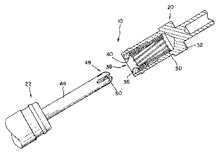
A preferred embodiment of the electrical conriector as shown in Figs. 1-4. In
the
illustrated embodiment, a female electrical conductor engages with a
corresponding male
l o connector as shown in Fig. 1 to form an electrical coupling. The
electrical coupling 10, in
generally comprised of two main components a female electrical connector 20
and a
corresponding male electrical connector 22. When the female connector and male
connector are axially mated together, electrical signals from two coaxial
cables may be
transmitted there between. In the Figs., the two coaxial cables are not shown.
The
15 electrical signals are transmitted by means of the inner and outer contact
structure of the
female electrical connector 20 coming into contact with the contact structure
of the
corresponding male electrical connector 22 when the male and female connectors
are
coaxially engaged.
Female electrical connector is constructed by a formation of resilient
conducting
2 o wires formed in a generally hyperboid shape 30 as known in the art and
from U.S. Patent
6,102,746 the disclosure of which is explicitly hereby incorporated by
reference. The
formation of contact wires 30 are pressed fit into the houaing 32 as shown in
Fig. 4. The
4
CA 02461041 2004-03-09
housing 32 also includes a location for connection to the contact lead, not
shown, such
connection location 34 into which the connecting leads may be fixed.
Electrical
connection between the connection location 34 and the interfit wire formation
30 is not
shown, but transfers through the interior of housing 32.
s Referring to Figs. 1 and 3a-c is a male electrical connector 22 of the
present
invention having a connection location 44 within a housing 42. The connection
location
44 permits an insertion of a connector lead, not shown, to thereby be in
electrical
communication with pin element 46.
Around the outer periphery of the hyperbolic connection 30 is located a solid
to arc-suppressing ring or portion 36 that is an electrical communication with
a formation of
hyperbolic contact wires 30.
The present invention relates to a particular geometry of the arc suppressing
ring
or portion 36 compared to the geometry of pin element 46. Arc arresting ring
or portion
36 has an opening 38 having a non-expanding inner surface 40. Arc suppressing
ring 36
15 IS formed of a solid metal or electrically conductive material.
The present invention includes the provision on pin element 46 of a collapsing
structure 48 that is larger in diameter than opening 38, such that during
insertion,
electrical contact is first made between pin 46 and female electrical
connector 20 at the
arc suppressing ring 36. After such contact has been created and any
electrical potential
2 o existing between the pin contact and socket are eliminated, the pin 46
enters into
formation of wires 30 and is seated therein. After the pin element 46 is fully
seated within
formation 30, no further electrical contact is made between arc arresfiing
ring 35 and pin
CA 02461041 2004-03-09
member 46. In other words, all communicating of electrical potential passes
through pin
46 through the formation of hyperbolic wire 30. This structure allows hot
plugging of the
assembly while a high electrical potential exists between tlne pin 46 and
female electrical
connector 20. This high electrical potential can result in arcing between the
pin and
s socket contact as they are brought into olose proximity.
In operation, as pin 46 is moved into or near contact with the socket contact,
the
initial arc is absorbed by the arc suppressing ring 36. In this fashion,
electrical arcing
between the pin 46 and thin wires of 30 are prevented. In more detail, the
geometry of
pin 46 is such that at in its distal end, a slot 50 is formed thereby forming
a collapsible
to structure 48 that allows passage of pin 46 past opening 38. Other
collapsible or shape
changing structures may be equivalently utilized. In the most preferred
embodiment of
the invention, the outside diameter of pin 46 at location B is greater than
the of interior
diameter of opening 38, surface 40.
The diameter of the pin 46 at other locations besidca 48 is smaller than the
inside
m diameter of 38.
After penetration of the collapsing structure and slot structure 48 and 50
into wire
formation 30, the geometry of pin 46 has a small diameter labeled as B. The
limitations
of diameter B of such that it is smaller than the diameter or opening of
opening 38 of
surface 40 thereby preventing electrical connection at that point. The
creation of the
2 o collapsing structure 48 and or slot 50 creates a spring loaded spark
arresting area on pin
46. Furthermore, the clearance between pin 46 and opening 38 (the difference
in
diameters between pin diameter B and surface 40) result:> in that the
electrical contact is
6
CA 02461041 2004-03-09
solely made within the receptacle basket or wire formation 30, eliminating the
potential for
fretting corrosion in vibrating environments at the arc-arresting portion. No
high normal
forces to the surface of pin 46 are experienced by or creaired by the arc
suppressing ring
36 because of the clearance formed therebetween. The prevention of such high
normal
forces as found in the art is advantageous under high vibrations conditions.
While this invention has been described as having a preferred design, the
present
invention can be further modified within the spirit and scope of this
disclosure. 'This
application is therefore intended to cover any variations, uses, or
adaptations of the
invention using its general principles. Further, this application is intended
to cover such
to departures from the present disclosure as come within known or customary
practice in
the art to which this invention pertains and which fall within the iimits of
the appended
claims.
7