Note: Descriptions are shown in the official language in which they were submitted.
CA 02461475 2004-03-24
WO 03/028403 PCT/CA02/01461
ALL-OPTICAL SWITCHING SITES FOR
AN AGILE OPTICAL NETWORK
TECHNICAL FIELD
The present invention relates to the field of
optical network switching site architectures, and, in
particular, to an all-optical add/drop site for use in an
agile optical network.
BACKGROUND OF THE INVENTION
Prior art all-optical networks include optical
fiber links between network elements that use wave division
multiplexing (WDM) or dense wave division multiplexing
(DWDM) to convey data over a plurality of channels. Each
optical fiber link may include a plurality of optical
devices, including amplifiers (commonly erbium doped fiber
amplifiers (EDFAs)) provisioned at fixed intervals between
the terminals, used to boost the channel signal intensities
of the plurality of channels. Each channel uses a narrow
band of wavelengths (that does not overlap the wavelengths
used by any other channel) to carry a signal. Channels are
routed through the optical fiber links at switching sites,
and originate/terminate at add/drop paths of add/drop
sites, etc. Each drop path receives a channel, and converts
a signal carried on the channel into a digital electrical
signal. The electrical signal may then be re-issued into
the optical network on any channel by an add path, issued
onto another. network (optical or other), or may be fed to a
signal processor. As is known in the art, the conversion
from optical to digital electrical signals, and then back
to optical signals (0E0 conversion) is time consuming,
power intensive, and limits the efficient use of optical
fiber link bandwidth. All-optical switches (switches that
CA 02461475 2004-03-24
WO 03/028403 PCT/CA02/01461
- 2 -
do not perform OEO conversion) can receive and transmit
many more channels than switches that perform OEO
conversion.
OEO conversion is the most reliable way to
regenerate a signal that has been degraded during
transmission through a channel over one or more optical
fiber links. OEO conversion also facilitates
cross-connection of signals. Once the signal has been
converted into a digital electrical signal, it can just as
easily be converted to any outgoing channel and sent on any
available output optical fiber link. The outgoing signal
will have no dispersion, signal power loss or distortion
when it is re-transmitted.
The distance between regeneration points (i.e., the
reach of a channel) may be extended using many known
techniques such as Raman pumping and forward error
correction encoding schemes. These techniques permit
channels to carry signals in all-optical networks over
distances far in excess of one optical fiber link. It is
therefore desirable to use all-optical switching to relay
signals over multiple optical fiber links.
Although all-optical networks are known in the
prior art, because of certain problems associated with the
propagation of optical signals over long distances, those
networks have limited reach and agility, and in their
bandwidth utilization. The reach of a network governs the
size of a geographical area that can be served by the
network. The agility of the network determines how readily
the network can be reconfigured to adapt to changes in the
data traffic within the area served by the network.
CA 02461475 2004-03-24
WO 03/028403 PCT/CA02/01461
- 3 -
All-optical networks that use standard optical
fiber may use only a small band in which wavelengths are
not subject to substantial chromatic dispersion. Using "C"
and "L" bands of wavelengths, on the other hand,
significantly many more channels of data can be conveyed
concurrently. The C and L bands, however, are subject to
chromatic dispersion in standard optical fiber. Chromatic
dispersion limits the distance over which a channel can be
carried on an optical fiber before regeneration, and hence
the distance data can be conveyed in an all-optical
network. The distance between regeneration points of prior
art all-optical networks that use the C and/or L bands are
severely restricted by chromatic dispersion.
In prior art all-optical networks, a bulk
dispersion slope compensation module (DSCM) is typically
used to compensate for local dispersion (dispersion
incurred as a result of transmission over one optical fiber
link). DSCMs are adapted to concurrently correct for
dispersion in all of the channels carried in an optical
fiber link, to within a predefined tolerance. The
predefined tolerance allows for some uncorrected dispersion
to remain across some of the channels. As the channels
traverse a plurality of optical fiber links without
regeneration, uncorrected dispersion remaining after each
optical fiber link accumulates, causing intra-channel
dispersion of the data carried in channels. Intra-channel
dispersion causes loss of signal quality (signal Q).
As is known in the art, the peak intensity of the
channel is conveyed on the center wavelength of the
channel, but some channel intensity is spread across
CA 02461475 2004-03-24
WO 03/028403 PCT/CA02/01461
- 4 -
neighboring wavelengths. These neighboring wavelengths are
received before or after the center wavelength because of
the chromatic dispersion. When the temporal spread of the
wavelengths exceeds a fraction of the bit interval (the
inverse of the bit rate) of the signal, the bit pulses of
data overlap each other, severely distorting the signal.
This intra-channel dispersion can exceed the tolerances of
receivers, rendering the signal carried on the channel
indecipherable. So, as the number of optical fiber links
that the channel traverses increases, so does uncorrected
dispersion and intra-channel dispersion. To permit the
number of optical fiber links traversed by a channel to be
extended, a mechanism for compensating for varying amounts
of dispersion in an adaptive manner is required.
Agility in an optical network with an all-optical
layer is also limited by phenomena called non-linearities
(such as Stimulated Raman Scattering, Cross-phase
modulation, Self-phase modulation, etc.). These non-
linearities result in the exchange of signal power across
adjacent channels. In an all-optical network these effects
must be controlled for signals that have traversed
different paths and may have a large disparity in signal
intensities.
In prior art optical networks that do not employ
all-optical switching, channels travel over point-to-point
optical fiber sections prior to regeneration. Consequently,
control feedback systems designed to balance signal
intensities on adjacent channels in such optical networks,
are used to control non-linearities. The channel
transmitters receive the control feedback information and
CA 02461475 2004-03-24
WO 03/028403 PCT/CA02/01461
- 5 -
adjust transmitted powers to optimize the signal to noise
ratio of the optical signal received at downstream
amplifiers, etc. In an all-optical network, channels are
dropped and added to optical fiber links in dependence upon
traffic patterns. These channels will traverse varying
lengths of optical fiber and have varying signal intensity
and net dispersion.
There therefore remains a need for an all-optical
switching site for use in WDM/DWDM optical networks that
performs all-optical switching and enables construction of
an agile optical network with improved reach.
OBJECTS OF THE INVENTION
Accordingly, an object of the present invention is
to provide all-optical switching sites for use in wave
division multiplexed (WDM) and dense wave division
multiplexed (DWDM) optical networks, that enables the
construction of an agile optical network.
Another object of the invention is to provide
all-optical switching sites that correct for dispersion
accumulated over a variable number of optical fiber links,
at each drop path.
A further object of the invention is to provide an
all-optical switching site adapted to provide intra-channel
signal intensity balance for channels conveyed through the
all-optical switching site. This is used to provide optimum
signal powers, signal to noise ratios, signal quality (Q),
and to minimize the effect of non-linearities in the output
fibers.
CA 02461475 2004-03-24
WO 03/028403 PCT/CA02/01461
- 6 -
SU1~2ARY OF THE INVENTION
Accordingly, the present invention provides an
all-optical switching site for an agile optical network
connected to at least one input optical fiber link and at
least one output optical fiber link, each of which
transport a plurality of wave division multiplexed (WDM),
or dense wave division multiplexed (DWDM) channels, the
all-optical switching site, C H A R A C T E R I Z E D by:
an optical add/drop multiplexer (ADM) having add
paths for adding channels to any of the at least one output
optical fiber links, and drop channels for extracting
. channel signals from any of the at least one input optical
fiber links;
an adaptive dispersion compensation module (ARCM)
in each drop path adapted to compensate for intra-channel
wavelength dispersion in a received dropped channel signal;
and
an optical transmitter for each add path.
In accordance with another aspect of the invention,
the all-optical switching site further includes an adaptive
dispersion control module (ADCM) in each drop path, the
ADCM being adapted to fine tune the dispersion compensation
of a signal carried on a received channel. Each ADCM is
preferably provisioned to receive a coarse-grain dispersion
compensation adjustment setting during the provisioning of
the channel switching, so that if the signal received at
the ADCM is changed from another signal having been carried
on a channel that has traversed a radically different
optical path, and consequently incurred a different amount
of net dispersion, the ADCM can be set to correct for an
approximate intra-channel dispersion of the new signal. The
CA 02461475 2004-03-24
WO 03/028403 PCT/CA02/01461
-
approximate residual dispersion may be calculated based on
one or more of the factors that affect dispersion,
including: the distance traversed over optical fiber links
of respective types, the amount of bulk dispersion slope
compensation in respective optical fiber links, and the
center wavelength of the channel.
Additionally, the ADCM is adapted to fine tune the
dispersion compensation with control feedback. The control
feedback will include a value of a parameter that varies
with dispersion, which could be a signal-to-noise ratio,
signal Q, a bit error rate (BER), a measure of a spectral
content, and/or a direct measure of dispersion.
Specifically, ~an "eye-closure" diagram, familiar to those
skilled in the art, used to optimize optical to electrical
conversion in the receiver, can measure the amount of
dispersion, or the signal quality and forward this data to
the ADCM. Alternatively, the ADCM can generate its own
control feedback, which avoids the re-provisioning of
incumbent receivers. In the alternative case, output of a
dispersion compensation element is tapped, to produce a low
power sample of the signal. The sample then undergoes
optical to electrical (OE) conversion in a manner known in
the art. The result of the OE conversion is that the
intra-channel dispersion of the signal is determined by
means such as spectral content. The intra-channel
dispersion is forwarded to an adaptive control, which
alters the amount of dispersion compensation applied to the
signal by the dispersion compensation element. The ADCM
would therefore further require a receiver and tap. In a
second alternative case, the sample could be directly
inspected without conversion to an electrical signal.
CA 02461475 2004-03-24
WO 03/028403 PCT/CA02/01461
_ g
Instead, an optical signal analyzer may be used to generate
the value of a parameter that varies with intra-channel
dispersion.
In accordance with another A method of compensating
for net dispersion of a signal transmitted over a variable
number of optical fiber links in a wave division
multiplexed/ dense wave division multiplexed optical
network, comprising steps of receiving a signal on a
channel of the optical network, analyzing a quality of the
received signal, measuring a quality of the received signal
and controlling a dispersion compensator to adjust the
signal in order to reduce intra-channel dispersion,
C H A R A C T E R I Z E D by:
receiving the signal on a dropped channel;
analyzing a quality of the received signal on the
dropped channel;
sending a measure of the quality of the signal on
the dropped channel to an adaptive controller (AC) of a
dispersion compensation element (DCE);
computing a dispersion compensation adjustment at
the AC using the measure of quality; and
controlling the DCE to apply the dispersion
compensation adjustment to the signal on the dropped
channel in order to reduce intra-channel dispersion of the
signal.
BRIEF DESCRIPTION OF THE DRAWINGS
Further features and advantages of the present
invention will become apparent from the following detailed
description, taken in combination with the appended
drawings, in which:
CA 02461475 2004-03-24
WO 03/028403 PCT/CA02/01461
_ g _
FIG. 1 is a schematic diagram illustrating
principal functional elements used in an all-optical
add/drop switch for a WDM optical network, known in the
art;
FIG. 2 is a schematic diagram illustrating
principal functional elements used in an all-optical
switching site in accordance with the invention;
FIG. 3 is a schematic diagram illustrating
principal functional elements used in an all-optical
switching site in accordance with the invention that
permits selected channel signals to bypass the PXC;
FIG. 4 is a schematic diagram illustrating
principal functional elements used in an all-optical
switching site in accordance with the invention that
performs limited cross-connection of channel signals
between two optical fibers;
FIG. 5 is a schematic diagram illustrating
principal functional elements used in an all-optical
switching site in accordance with the invention that
cross-connects channel signals between two respective
optical fibers; and
FIG. 6 is a schematic diagram illustrating
principal functional elements used in an adaptive
dispersion compensation module (ARCM) in accordance with
the present invention.
It should be noted that, throughout the appended
drawings, like features are identified by like reference
numerals.
CA 02461475 2004-03-24
WO 03/028403 PCT/CA02/01461
- 10 -
DETAILED DESCRIPTION OF THE PREFERRED EMBODIMENT
The invention enables all-optical switches to be
incorporated into WDM/DWDM optical networks to form agile
optical networks with improved reach, agility and channel
capacity. An agile optical network is, for the purpose of
this invention, a readily re-configured WDM/DWDM
all-optical network adapted to perform all-optical
switching of channels, the wavelengths of which fall within
a dispersive band, and may extend over a plurality of
optical fiber links.
FIG. 1 illustrates an all-optical add/drop switch
incorporating an optical add/drop multiplexer, for use in a
WDM optical network that is known in the art. The all-
optical add/drop switch comprises a demultiplexer 18
adapted to separate a bulk optical signal received on an
input optical fiber link 11 into component channels, in a
manner known in the art. Each channel is then switched by a
photonic cross-connect (PXC) 20 to either a corresponding
output channel, or a drop path 24. The PXC 20 also switches
added channels from respective add paths 22 to
corresponding output channels. The output channels are
multiplexed by a multiplexer 26 to form a bulk output
optical signal transmitted on the output optical fiber link
11'.
As is known in the art, there may be a plurality of
input and/or output optical fiber links terminated at the
all-optical switching site, the only limit being that
imposed by the switching capacity of the PXC 20. It is also
known in the art to amplify the received optical signal
before and/or after the PXC, and to perform bulk dispersion
CA 02461475 2004-03-24
WO 03/028403 PCT/CA02/01461
- 11 -
compensation of the bulk optical signal prior to
demultiplexing, or after multiplexing.
Each of the add paths 22 is equipped with a
transmitter 23, which may be a tunable laser, or any other
means for emitting modulated optical signals on one channel
at one time, and later on another channel. Each of the drop
paths are equipped with a respective receiver 25, which
includes a photodetector adapted to absorb the incident
channel signal's light, and convert the signal into an
analog electrical signal, and a circuit for discriminating
1' s and 0' s . Both the add and drop paths may be connected
with an OEO switch that is adapted to regenerate a
channel's signal. The dropped signal may be returned to the
all-optical layer on the same or any other available
channel; it may be switched to another network; or it may
be received and processed by the receiver's processor.
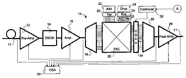
FIG. 2 illustrates an optical switching site 10 in
accordance with the present invention. An input optical
fiber link 11 carrying wavelength division multiplexed
optical signals is first amplified by a pre-amplifier 12.
The bulk optical signal (the aggregate of multiplexed
channels) is then dispersion corrected, by a dispersion
slope compensation module (DSCM) 14. The bulk optical
signal is then amplified by a power amplifier 16, and sent
to a de-multiplexes 18. The de-multiplexes 18 separates the
bulk signal into respective channels, which are sent, in
parallel, to the PXC 20. The PXC 20 switches the respective
channels and a set of added channels (received from
transmitters 23 of respective add paths 22), to output
channels and drop paths 24. Prior to transmission over the
CA 02461475 2004-03-24
WO 03/028403 PCT/CA02/01461
- 12 -
optical fiber link 11', the output bulk optical signal is
amplified by post-amplifier 28, in order to boost the
channel powers of the constituent channel signals.
Two devices are further added to provide the
all-optical switching site 10 in accordance with the
invention. An adaptive dispersion compensation module
(ADCM) 32 is added to each drop path 24 connected to the
PXC~20, to perform dispersion compensation on an individual
channel. This will compensate for dispersion accrued over a
variable number of optical fiber links traversed by the
channel, prior to optical fiber link 11, for which the DSCM
14 does not compensate. The operation of the ADCM 32
control is further discussed with reference to FIG. 6.
The DSCM 14 corrects for a mean dispersion of all
channels carried by the optical fiber link 11. The DSCM 14
therefore cannot compensate for channel dependent
dispersion, if different channels have followed different
optical paths. Receivers in the cross-connect 20 are
usually adapted to tolerate a limited amount of
intra-channel dispersion.
The pre-amplifier 12 and power amplifier 16 are
used to boost the bulk optical signal, prior to
de-multiplexing, as they are presumed to be required for
the present embodiment. An optical spectrum analyzer
(OSA) 30 is used to dynamically adjust the gain settings of
the pre-amplifier 12, the power amplifier 16, and the post-
amplifier 28 using per wavelength measurement of power
and/or a signal to noise ratio. There may be any number of
amplifiers and amplifier control systems (such as the OSA)
in different embodiments depending on; the strength of the
CA 02461475 2004-03-24
WO 03/028403 PCT/CA02/01461
- 13 -
signals entering the all-optical switching site 10 in
respective channels, a loss of signal strength incurred
during transit through the all-optical switching site 10,
and the signaling requirements for transmission on optical
fiber link 11'. The bulk optical signal is tapped before,
after, or before and after each amplifier (in this case the
pre-amplifier 12 the power amplifier 16, and the post-
amplifier 28) that the OSA controls. As is known in the
art, tapping involves removing a portion of the bulk
optical signal, and sending the low intensity sample of the
bulk signal along a separate optical path, in this case, to
the OSA 30. These bulk signals are compared to determine
the differences in spectral qualities of the bulk optical
signal before and after amplification. The comparison is
used to adjust the gain settings of the pre-amplifier 12,
the power amplifier 16, and the post-amplifier 28.
The second new device included in the all-optical
switching site 10 shown in FIG. 2, is a variable optical
attenuator (VOA), controlled by a controller 35. Each of
the VOAs 34 interfaces a respective one of the
de-multiplexed channels. The VOAs 34 in FIG. 2 are located
immediately prior to multiplexing, enabling control of
intra-channel signal intensity balance in order to optimize
performance on outbound optical fiber link 11' upon which
the channels are conveyed. The control of the VOAs 34
involves receiving feedback from a downstream signal
analyzer that calculates channel signal intensity balance,
and issues a message to the controller 35. The
controller 35 uses the feedback to determine changes to the
attenuation of individual channels, and uses control
signaling to effect the changes.
CA 02461475 2004-03-24
WO 03/028403 PCT/CA02/01461
- 14 -
A second embodiment incorporating a PXC 20 into an
all-optical switching site 10 is illustrated in FIG. 3. In
accordance with the second embodiment, a predefined set of
channels are provisioned as by-pass channels, while the
remainder are provisioned as add/drop channels. The
add/drop channels are terminated at the PXC 20 and are
switched to either a respective drop path, or a
corresponding output channel. Added channels are switched
to corresponding output channels. Signals carried on the
by-pass channels do not incur the insertion loss caused by
transport across the PXC 20, as they are not switched. As
is known in the art, the size and configuration of optical
switches determines the signal intensity loss incurred as a
signal is conveyed through the switch (generally referred
to as insertion loss).
As illustrated in FIG. 4, an all-optical switching
site 10 may interconnect two (or more) optical fiber links
(lla-lla',llb-llb') in a limited manner. A set of transfer
add/drop paths 36 are used to switch channels from the
input optical .fiber link lla to output optical fiber
link 11b', and another set of transfer add/drop paths 36'
are used to switch from llb to 11a'. The amount of
insertion loss of a PXC generally depending on technology
used and the number of switched channels. Smaller PXCs
generally have less insertion loss than larger PXCs.
Consequently, the use of two smaller PXCs in lieu of a
larger PXC reduces insertion loss at the site 10. The
number of channels available for switching is equal to the
number of transfer add/drop paths 36, 36'.
CA 02461475 2004-03-24
WO 03/028403 PCT/CA02/01461
- 15 -
The VOAs 34a,b illustrated in FIG. 4 are located
upstream of the PXCs 20a,b. This is a viable configuration
provided that control processes for the VOAs 34a,b are
adapted to compensate for the position of the VOAs 34a,b.
If a channel (chl) is switched from lla to 11b', for
example, attenuation of the chl has to be performed by a
VOA in VOAs 34a. Furthermore, if a channel (ch2) is added
to the optical fiber link 11a', the signal strength of the
ch2 must be controlled through the transmitter 23a or 23b
in the add path. Consequently, controller 35 preferably
controls VOAs 34a, VOAs 34b, and transmitters 23a,b, in
response to control feedback received from components of
11a' and 11b'. Alternatively, at the time that the PXC 20
is provisioned to perform switching through a transfer
add/drop path 36, 36' (to transfer a channel from lla
to 11b', for example), a controller 35b (FIG. 5) can be
programmed to forward the channel signal intensity balance
feedback to a controller 35a. In this configuration, the
controller 35a also sends control information to the add
path transmitters of PXC 23a based on channel signal
intensity balance feedback received from controller 35a, if
an added channel is to be switched to 10b'.
The pre-amplifiers l2a,b and power amplifiers l6a,b
are controlled by OSAs 30a,b, respectively, and a separate
OSAs 30a',b' are used to control post-amplifiers 28a,b
respectively, in the third embodiment. The use of two
separate amplifier controllers is particularly useful when
the all-optical switching site 10 has a high insertion loss
requiring two more amplifiers on output optical fiber links
lla',b'.
CA 02461475 2004-03-24
WO 03/028403 PCT/CA02/01461
- 16 -
As illustrated in FIG. 5, a plurality of optical
fiber links can be cross-connected by a PXC 20. The PXC 20
can switch channels from input optical fiber link lla to
output optical fiber link 11b', .or from llb to 11a', as
long as the wavelengths of channels launched on an output
optical fiber link (11a' or 11b') do not overlap. In order
to switch a signal that was received on one channel to an
output optical fiber link that already carries a wavelength
overlapping channel, the switched channel has to be
converted to an unused wavelength band. As many optical
fiber links can be added as the PXC can support. PXCs with
the ability to switch a greater number of channels,
however, may incur greater insertion loss, and therefore
limit the reach of the channels passing therethrough.
Another range limiting factor associated with PXCs is
redundancy. Some PXCs are configured to split and recombine
channels as a failsafe precaution. Thus, double the
switching capacity of the PXC is required to provide full
redundancy, in comparison with the switching capacity of a
non-redundant PXC. The PXCs of any of the embodiments
described previously can be configured as either redundant
or non-redundant switching sites.
In general, the greater the insertion loss, the
greater the number of on-site amplifiers required to
maintain channel signal intensity. Given that there is a
limit to how many times a signal carried on a channel can
be amplified before regeneration is required; there is a
trade-off between cross-connecting many channels and the
distance over which each of the many channels may be
propagated prior to regeneration.
CA 02461475 2004-03-24
WO 03/028403 PCT/CA02/01461
- 17 -
FIG. 6 is a schematic diagram of an ADCM 32 in
accordance with the invention. The ADCM 32 is adapted to
apply dispersion compensation to a received signal,
depending on an estimated or observed signal dispersion.
The ARCM 32 includes a dispersion compensation element
(DCE) 38 adapted to apply a controlled amount of dispersion
compensation to a received signal. The DCE 38 may be a
virtually imaged phase array (VIPA) or a fiber Bragg
grating (FBG) device, for example, each of which is known
in the art. The ADCM 32 also includes an adaptive
controller 40 enabled to control the amount of dispersion
compensation applied by the DCE 38. The adaptive
controller 40 may be configured to compute a coarse-grained
signal dispersion adjustment setting based on an estimate
of a dropped channel's net dispersion. The estimate is
preferably based on information communicated to the
adaptive controller 40 by an agile network controller (not
shown). The coarse-grained signal dispersion adjustment is
applied before feedback related to the signal is available.
The coarse-grained signal dispersion adjustment may be
computed using any one or more of several parameters
communicated to, or stored by, the adaptive controller 40.
The parameters may include, but are not limited to: a
distance that the optical signal has traveled through the
network; the type of optical fiber links over which the
signal has been conveyed; the channel's center wavelength
and, an amount of dispersion compensation applied to the
channel a last time the channel was dropped to the ADCM 32.
Thereafter, the adaptive controller 40 receives control
feedback respecting the intra-channel dispersion of the
signal the ADCM 32 outputs and, when applicable, directs
CA 02461475 2004-03-24
WO 03/028403 PCT/CA02/01461
- 18 -
the DCE 38 to adjust the dispersion compensation applied to
the signal.
In accordance with the embodiment illustrated in
FIG. 6, the receiver (Rx) 42 generates the control
feedback, and sends the control feedback to the adaptive
controller 40. An isolator 44 may be added to prevent
reflected signal intensity from interfering with upstream
network elements.
The control feedback preferably includes a measure
of a parameter that is related to signal dispersion. One
example of such a measure is signal quality (Q), which is
readily measured by an eye-closure diagram generated by the
receiver (Rx). Other parameters include a signal-to-noise
ratio (SNR) of the received signal; a signal dispersion
measure; a spectral content analysis; and, a bit error rate
(BER) associated with data encoded by the signal, all of
which are well known in the art. Alternatively, a sample of
the signal can be tapped from the output of the DCE 38, and
sent to a dispersion measurement device. The dispersion
measurement device 46 directly or indirectly measures the
dispersion of the signal, either by optical measurements,
or OE conversion using a second receiver. An' advantage of
the dispersion measurement device 46 is that incumbent
receivers 42 do not have to be re-provisioned to provide
the control feedback to the adaptive controller 40. In
certain receivers, however, it may be more efficient to
re-use the measures of signal quality, etc. generated by
the receiver 42 to generate the control feedback.
The invention therefore provides a versatile
all-optical switching site 10 for an agile optical network
CA 02461475 2004-03-24
WO 03/028403 PCT/CA02/01461
- 19 -
that permits a channel to be selectively dropped using an
adaptive dispersion compensation module 32 to compensate
for channel dispersion in response to feedback signals
indicative of signal quality, or the like. The all-optical
switching site 10 likewise permits channels to be added by
controlling generated signal intensity by tunable optical
transmitters 23 while balancing signal strength using
variable optical attenuators (VOAs) 34. The all-optical
switching site 10 can be overlaid on an electrical cross
connect, or used in a stand-alone configuration.
The embodiments of the invention described above
are intended to be exemplary only. The scope of the
invention is therefore intended to be limited solely by the
scope of the appended claims.