Note: Descriptions are shown in the official language in which they were submitted.
CA 02461886 2004-03-26
WO 03/028146 PCT/US02/31118
ELECTRICALLY TUNABLE BANDPASS FILTERS
BACKGROUND
Related Applications
This application claims the benefit of provisional U.S. Application
Serial No. 60/325,701, entitled "ELECTRICALLY TUNABLE
BANDPASS FILTERS," filed September 27, 2001, and provisional U.S.
Application Serial No. 60/XXX,XXX, entitled ELECTRONICALLY
TUNABLE FILTERS/PASSIVES PROPOSAL, filed September 23, 2002,
both of which are incorporated herein by reference in their entirety for all
purposes.
Field
This invention relates generally to electronic filters. More
specifically, this invention is directed to electrically tunable bandpass
filters.
Due to increasingly crowded frequency allocations, modern wireless
communication devices require increasingly stringent filtering
specifications. This is particularly true for devices that operate in multiple
modes and/or over multiple frequency bands. Devices now popularly in
use employ fixed tuned bandpass filters (BPF) which have design
tradeoffs. The design goals of low passband insertion loss (IL) and high
close-in rejection conflict. Portions of the filter transfer function
representing the edges of the passband have a finite slope (the passband
CA 02461886 2004-03-26
WO 03/028146 PCT/US02/31118
2
cutoff is gradual rather than an ideal perfectly abrupt transition from 'pass'
to 'no-pass' ). The more sharp the cut off required, the higher the order of
the filter must be. Higher order filters are more bulky and have a greater
IL than lower order filters and may require extensive turning to meet
specifications. To meet the out-of band rejection specifications, typical
filter designs require a transmission zero, requiring a filter vendor to tune
each filter during its manufacture. Multiple filters are typically required
for mufti-band, mufti-mode operation. In spite of this, often filter
specifications are not met, resulting in accepting non-compliant parts with
increased IL or inadequate rejection, or using split band designs, which
require extra switches and have greater IL.
Unlike a fixed tuned BPF, a tunable filter can be dynamically tuned
to different frequency ranges within a specific band, and if sufficiently
tunable, different frequency ranges within multiple bands. Tunable filters
have several advantages over non-tunable filters. For example, tunable
filters need not have a broad passband if the passband is dynamically
adjustable. A narrow transfer function with high close-in rejection can be
implemented with a lower order filter than can a wide transfer function
with similar close-in rejection. Therefore, unlike a fixed tuned BPF, a
tunable filter can be of a lower order and still meet desired rejection
specifications. Lower order tunable filters are smaller in size, have a lower
profile, lower IL, and can be built using lower precision components using
a simpler fabrication processes, which in turn lowers cost. In addition, one
filter topology can be optimized to cover multiple bands if the tuning range
is wide enough. Thus multiple filter designs are no longer needed. Also,
split-band designs along with the associated switches become unnecessary.
Fig. 1 shows a typical implementation of a top coupled BPF 100.
One or more resonators 106 are coupled to an input 102 and an output 104
CA 02461886 2004-03-26
WO 03/028146 PCT/US02/31118
3
via capacitors 108. Other realizations are also possible. The resonators are
constructed and arranged so as to have a reactance that has at least one
resonant frequency. At frequencies below 200 - 300 MHz. the resonators
can be constructed from discrete components (i.e. separate capacitors and
inductors). Tuning involves changing the resonant frequency of the
reactance by changing the values of the discrete components. At higher
frequencies a more distributed layout is required because the inherent
reactances of all circuit components become more significant at higher
frequencies. At higher frequencies, resonators utilizing a monoblock
design are commonly used.
A high frequency resonator is essentially a transmission medium
with impedance discontinuities at both of its ends. Reflections at these
discontinuities causes energy to build up within the resonator, a fraction of
which is released during each cycle. A quality factor, Q, is defined as the
ratio of the energy stored within the resonator to that dissipated during one
cycle. Due to boundary conditions that must be obeyed by the electric and
magnetic fields, only signals with wavelengths that divide the length of the
resonator by certain discrete multiples will be maximally reflected and
constructively interfere. These correspond to the resonant frequencies.
Typically, the resonator is made sufficiently short such that only one
resonant frequency exists within the frequency range to be filtered. Signals
at other frequencies are increasingly transmitted to ground as their
frequency difference from the resonance frequency increases, resulting in
significant signal attenuation outside the passband.
The wavelength at a particular frequency within a particular
transmission medium is a function of the reactance of that medium. The
resonant frequency is changed by changing the length of the resonator as
measured with respect to the wavelength of the signal such that the
CA 02461886 2004-03-26
WO 03/028146 PCT/US02/31118
4
constructive interference underlying resonance occurs at the new resonance
frequency. Electrical tuning can be accomplished either by changing the
functional dependence of the local wavelength on the frequency or by
changing the electrical length of the resonator.
The wavelength dependence on frequency within a transmission
medium is a function of the reactance of the medium. This functional
dependence of the wavelength is varied in YIG (Yttrium-Iron Garnet)
resonators with the application of a variable magnetic field. But such
resonators are expensive, require bulky magnetic field generating coils, and
are unsuited for the low power, low profile, low cost requirements of
mobile communication systems.
Another approach utilizes a bulk, single crystal ferroelectric (f e)
waveguide as a resonator, where an applied voltage across the body of the
crystal is used to generate an electric field within .the waveguide, thereby
changing the dielectric constant of the crystal and hence its resonant
frequency (see US Patent No. 5,617,104). However, the loss tangent of
known f-a materials are poor compared to typical microwave ceramics.
This means that the reactance of the material contains a non-negligible
resistive component (i.e. an imaginary component to the dielectric
constant), resulting in significant power loss via resistive heating of the
material. As a result usage of bulk ferroelectric materials for resonators at
GHz and sub-GHz frequencies are currently impractical for many
applications. This does not preclude the use of ferroelectric films, but
heretofore no prior art has disclosed or suggested the adaptation of such
films to provide electrical tuning of electronic filters.
Further, bulk f a resonators may require the application of rather
high control voltages considering the relatively large geometries involved.
As previously mentioned, electrical tuning can also be accomplished by
CA 02461886 2004-03-26
WO 03/028146 PCT/US02/31118
changing the electrical length of the resonator. This is accomplished in the
prior art via the use of varicaps in which one or more varactor diode is
coupled to one end of the resonator. This arrangement electrically extends
that end of the resonator because the capacitance of the varactor prevents
that end from being either totally closed or totally open. Varactors provide
a variable capacitance as a function of an applied do voltage, and therefore
changes the length of the resonator in response to changes in the voltage.
But they are noisy, temperature dependent and have low Q's at UHF and
above. They are also limited as to how they can be employed in a filter.
They are too lossy to be put in parallel with a resonator and difficult to
implement within a distributed design. In addition their capacitive values
are relatively low and not very consistent from lot-to-lot.
SUMMARY OF THE INVENTION
The invention is a tunable bandpass filter comprising: at least one
resonator having a reactance with a resonant frequency, a ferroelectric f-a
film having a dielectric constant with a value that changes with an applied
electric field, and an electric field generating device for generating
relatively constant electric fields of different strengths. The ferroelectric
film is electrically coupled to the resonator so that the reactance of the
resonator and therefore the resonant frequency of the resonator and the
passband of the filter depends on the dielectric constant of the ferroelectric
film. The electric field generating device is constructed and arranged to
generate relatively constant electric fields within the ferroelectric film,
thereby making the resonant frequency of the resonator and the passband
CA 02461886 2004-03-26
WO 03/028146 PCT/US02/31118
6
of the filter a function of the strength of the relatively constant electric
field.
BRIEF DESCRIPTION OF THE DRAWINGS
Fig. 1 shows a typical implementation of a bandpass filter utilizing
multiple coupled resonators.
Fig. 2 is a diagram of a microstrip resonator utilizing the f a film.
Fig. 3 is a diagram of a first example of a stripline resonator utilizing
the f a film.
Fig. 4 is a diagram of a dielectric loaded waveguide resonator
utilizing the f a film.
Fig. 5 is a diagram of a second example of a stripline resonator
utilizing the f a film.
Fig. 6 is a diagram of an overlay capacitor coupled resonator
utilizing the f a film.
Fig. 7 is a diagram of an interdigitated filter topology.
Fig. 8 is a diagram of an interdigitated filter topology utilizing
overlay capacitors.
Fig. 9 is a diagram of a combline filter topology utilizing overlay
capacitors.
Fig. 10 is a table generally illustrating some of the design options,
benefits and issues associated with a variety of f-a device designs.
CA 02461886 2004-03-26
WO 03/028146 PCT/US02/31118
7
DETAILED DESCRIPTION
The relative permittivity, ~r, which determines the dielectric constant
of a dielectric may be varied in f a materials under the application of a
slowly varying ("near DC") electric field (E-field). And although the loss
tangent of bulk f a dielectrics is significant, that of applicable f-a thin or
thick films fabricated on a wide range of microwave ceramics may be
much better, approximating that of some commonly used microwave
ceramics. Therefore, rather than use a varactor or bulk f-a dielectrics for
electrical tuning, thin f a films may be used to modify the local capacitance
of the transmission medium and thereby provide an adjustable reactance
that changes the resonant frequency of the resonator. When properly
designed and fabricated, these f-a capacitors may provide a higher
capacitance and Q than varactors at frequencies above 1 GHz. They are
available as thin or thick films and are ideal for tuning distributed or
lumped element resonators. Their electrical properties from lot-to-lot are
also more consistent than that of varactors.
Thin/thick f a films are widely used in high temperature
superconductivity work, and there are several hundred of such known
materials. Film thicknesses on the order of 0.1 hum to 1 mm are typical.
Barium strontium titanate, BaXSr~l_X~Ti03 (BSTO) is the most popular for
room temperature operation where x is preferably between 0.3 and 0.7.
Their tuning speed is about 0.3 - 1.0 bus for an applied constant E-field, so
they are not modulated by a rf signals. An applied do voltage Vd~ is
generally used to create the E-field. It is not uncommon to have films with
O~r/OVd~ > 3.
CA 02461886 2004-03-26
WO 03/028146 PCT/US02/31118
8
Fig. 2 is an example of a microstrip resonator 200 comprised of a
microstrip filament layer 202, a ground plane 204, and a dielectric
substrate 206. A f-a film layer 208 is positioned between the microstrip
filament layer and the dielectric substrate. The wavelength of a propagated
signal is a function of the dielectric constant of the transmission medium of
the resonator and is therefore a function of the relative permittivity of the
f
a film 208. A voltage applied by a do voltage source 210 positively biases
the microstrip filament 202 with respect to the ground plane 204, and
creates an electric field (E-field) 212 across the f a film that changes ~ of
the film and therefore the resonant frequency of the resonator. The voltage
is controlled by external control signal 214.
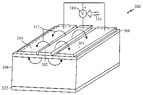
Fig. 3 is a first example of a coplanar waveguide 300 comprised of a
central conductor 302, two grounded outer conductors 304, a ground plane
322, and a dielectric substrate 306. An f-a film layer 308 is positioned
between the stripline conductors 302 and 304, and the dielectric substrate.
A voltage applied by the do voltage source 310 positively biases the central
conductor with respect to the two outer conductors and creates an electric
field (E-field) 312 across the f a film, but in this case the choice of bias
arrangement is better than that of Fig. 2 because the E-field 312 is more
concentrated within the f-a film and is therefore greater for the same
voltage and substrate thickness. The voltage is controlled by external
control signal 314.
Fig. 4 is an example of a dielectric loaded waveguide (DLWG)
resonator filter 400. An input signal introduced via input port 416
resonates at the resonant frequency within a first half of the waveguide 424
and is coupled via 2°d order aperture 420 to a second half of the
waveguide
426, which having the same resonant frequency, combine to form a second
order filter. An output signal is taken via output port 418. The body of the
CA 02461886 2004-03-26
WO 03/028146 PCT/US02/31118
9
filter, formed on substrate 406, is comprised of a high Er dielectric 402. An
f-a film 408, shown mounted on the surfaces parallel to the x-y plane at the
aperture, is overlaid by conducting planes 422. A voltage applied between
the two conducting planes 422 generates an E-field within the f-a film 408
that changes its reactance, resulting in a change of the resonant frequency
within the waveguide. The voltage applied by do voltage source 410 is
controlled by control signal 414. The f-a film 408 and conducting planes
422 could also be mounted on the surfaces parallel to the x-y plane. With
no external load, a DLWG resonator can provide a Q of about 1000 within
the PCS band (i.e. around 2 GHz) with an LL. of about 1.6 dB at a 3dB
bandwidth of 10 MHz.
Fig. 5 shows a second example of a stripline resonator 600
comprised of a central conductor 602, two grounded outer conductors 604,
and a dielectric substrate 606. The f-a film 608 is mounted between the
central conductor 602 and the dielectric substrate 606. A do voltage source
610 controlled by control signal 614 is applied between the central
conductor 602 and the two outer conductors 604 so as to generate an E-
field within the f-a film and thereby dynamically adjust the resonant
frequency of the resonator 600. With no external load, a stripline resonator
can provide a Q of about 750 within the PCS band with an LL. of about 2.2
dB at a 3dB bandwidth of 6 MHz.
Filter tuning with f-a films can also be implemented according to a
similar scheme as that described for tuning with varactors where tuning is
accomplished by adjusting the effective electrical length of one end of the
resonator. Instead of mounting the f-a film within the coax, stripline, or
microstrip resonators as shown in Figs. 2, 3 and 5, the film is coupled to
the transmission medium by mounting it as an overlay capacitor as
illustrated for the overlay capacitor coupled resonator 700 shown in Fig. 6.
CA 02461886 2004-03-26
WO 03/028146 PCT/US02/31118
The basic resonator 701, which can be coaxial, stripline or microstrip, is
mounted atop a ceramic substrate 706 with an underlying rf ground plane
704. An f a film layer 708 of thickness d is positioned towards one end of
the resonator and sandwiched between the resonator's grounded outer layer
and an overlaid metal layer 722, thereby forming the overlay capacitor.
Coupling to such a resonator can be achieved by either electromagnetic
coupling, capacitive coupling, or by a direct tap into and out of the
resonator (or filter) structure. F-a thin film layers of about 1 micro-meter
seem to provide high do R fields for a given (small) do voltage. For an
inductively coupled input signal, both ends of the resonators inner
conductor 702 can be grounded as shown. A do voltage source 710
controlled by control signal 714 generates the E-field used to adjust the
capacitance of the overlay capacitor.
Direct f 2 thin film deposition can be done on some substrates, or
with buffer layers on others. The packaging of an f 3 device may eliminate
the need for a substrate.
As shown in Fig. 1, multiple resonators can be electrically coupled
to obtain a higher order filter with a filter transfer function that, while
centered about the same resonant frequency as that of the resonator, has a
more abrupt cutoff and a flatter peak than each individual resonator's
transfer function. A number of different filter topologies utilizing different
resonator types are possible. Popular topologies utilizing stripline and
microstrip resonators include interdigitated filters, combline filters, and
edge coupled and hairpin filters. Fig. 7 is the top view of an example of an
interdigitated filter topology utilizing f a film electrical tuning in which
the
wavelength-frequency relationship within the resonator is varied. The
input signal via transmission line 802 is electromagnetically coupled to
each resonator in turn as it travels across the resonators (vertically in the
CA 02461886 2004-03-26
WO 03/028146 PCT/US02/31118
11
figure), and is output via transmission line 806. Each resonator has one
capacitively loaded and one shorted end. The relative placement of which
is alternated for adjacent filter. The resonance frequency of the resonator is
electrically adjusted as described above for f a film electrical tuning
utilizing the wavelength-frequency relationship adjustment.
Fig. 8 shows the same topology as that of Fig. 7 but with tuning
achieved via the use of overlay capacitors 908 coupled to what would
otherwise have been the open end of the resonators 904.
Fig.. 9 is the top view of an example of a second order
electromagnetically coupled planar combline filter topology utilizing
overlay capacitors 1008. The signal input via transmission line 1002 is
electromagnetically coupled to each resonator in turn as it travels across
the resonators 1004 (horizontally in the figure), and is outputted via
transmission line 1006. Such a filter may have a 10 mhz bandwidth in the
PCS band. With a 20 mil thick Mg0 substrate, no buffer layer may be
needed.
The structure of the resonators is not limited to that shown in Figs.
2-6. Any resonator structure where an f-a film is coupled to the
transmission medium is contemplated by the invention. For instance,
instead of being mounted within the resonator as shown in Fig. 5, the f a
film could be mounted on one or more outside surface of the coaxial or
stripline resonator similarly to the arrangement shown in Fig. 4 for the
DLWG resonator. Likewise, the f a layers need not be limited to coupling
apertures of the DLWG shown in Fig. 4. Instead, f a film can be deposited
on the I/O (Input/output) surfaces on the waveguide as well as on one or
more surfaces on the outside. Additionally, instead of using just one
overlay capacitor as shown in Fig. 6, two or more overlay capacitors can be
used at either or both ends of the resonator. Fig. 10 is a table generally
CA 02461886 2004-03-26
WO 03/028146 PCT/US02/31118
12
illustrating some of the design options, benefits and issues associated with
a variety of f-a device designs. Designs 3, 4, and 5 generally range from
minimum insertion loss, maximum size to minimum size maximum
insertion loss.
It can thus be appreciated that the objectives of the present invention
have been fully and effectively accomplished. The foregoing specific
embodiments have been provided to illustrate the structural and functional
principles of the present invention and is not intended to be limiting. To the
contrary, the present invention is intended to encompass all modifications,
alterations, and substitutions within the spirit and scope of the appended
claims.