Note: Descriptions are shown in the official language in which they were submitted.
CA 02462134 2009-09-30
. V =
CURRENT DRIVE CIRCUIT AND DRIVE METHOD THEREOF,
AND ELECTROLUMINESCENT DISPLAY APPARATUS USING
THE CIRCUIT
Technical Field
The present invention relates to a current drive
apparatus, a drive method of the current drive
apparatus, and a display apparatus using the current
drive apparatus, and more particularly to a current
drive apparatus including a structure to operate a
plurality of loads by applying a predetermined current
thereto, a drive method thereof, and a display
apparatus which displays desired image information in a
display panel by using the current drive apparatus.
Background Art
Conventionally, there is kiiowri a light emitting
element type display including a display panel in which
a plurality of organic electroluminescence elements
(which will be referred to as "organic EL elements"
hereinafter), inorganic electroluminescence elements
(which will be referred to as "inorganic EL elements"
hereinafter), or self-luminous type light emitting
elements (optical elements) such as light emitting
diodes are arranged in a matrix form.
As compared with a liquid crystal display (LCD)
which has considerably spread in recent years, such a
light emitting element type display has a higher
CA 02462134 2004-03-26
WO 2004/003877 PCT/JP2003/008153
2
display response speed and no field angle dependency,
an increase in contrast, realization of high definition
of a display image quality and a reduction in power
consumption are possible. Further, a reduction in
thickness and weight of one layer is possible since it
does not require a back light as different from the
liquid crystal display. Thus, it has a very excellent
characteristic, so that the light emitting element type
display has been studied and developed vigorously as a
display of the next generation.
Such a display generally includes a display panel
in which display pixels including light emitting
elements are arranged in the vicinity of respective
intersects of scanning lines arranged in a row
direction and data lines arranged in a column
direction, a data driver which generates a predeter-
mined drive current according to display data and
supplies it to each display element through the data
lines, and a scanning driver which causes display
pixels in a predetermined row to enter a selection
state by applying a scanning signal with a predeter-
mined timing. In such an apparatus, by causing each
light emitting element to perform the light emitting
operation with a predetermined brightness gradation
according to the display data by using the drive
current supplied to each display pixel, desired image
information is displayed in the display panel. A
CA 02462134 2004-03-26
WO 2004/003877 PCT/JP2003/008153
3
concrete example of the light emitting element type
display will be described in detail in conjunction with
a later-described embodiment.
Here, in the display drive operation in the
display, there are known a current specification type
drive mode which sequentially repeats in accordance
with each row for one screen the operation which
generates drive currents having individual current
values according to the display data with respect to a
plurality of display pixels, simultaneously supplies
the currents to the display pixels in a specific row
and causes the light emitting element of each display
pixel to emits the light with a predetermined
brightness gradation, and a pulse width modulation
(PWM) type drive mode which sequentially repeats for
one screen the operation which supplies drive currents
having a fixed current value with individual time
widths (signal widths) according to the display data
relative to a plurality of the display pixels to the
display pixels in a specific row in the same display
period and causes each light emitting element to emit
the light with a predetermined brightness gradation.
In these display drive operations, the drive
currents having predetermined current values or a fixed
current value according to the display data must be
supplied to a plurality of the display pixels in each
row at the same time or within the same display period.
CA 02462134 2004-03-26
WO 2004/003877 PCT/JP2003/008153
4
In order to cope with realization of high definition
and a large screen of a thin display device in recent
years, there is known a display having applied thereto
a circuit configuration which includes a plurality of
driver chips (semiconductor chips) each having a
predetermined number of output terminals as the above-
described data drivers, individually generates the
drive currents in the respective driver chips and
supplies the drive currents to the respective light
emitting elements through a data line at the same time.
The display to which the above-described data
driver including a plurality of the driver chips is
applied has the following problems.
The conventional data driver having a plurality
of the driver chips includes a circuit used to
individually generate a drive current in accordance
with each driver chip and has a structure to simultane-
ously supply the drive currents to the respective light
emitting elements from the respective driver chips
through respective output terminals. Therefore, when
irregularities are generated in current values of the
drive currents outputted from a plurality of the driver
chips, irregularities occur in the light emitting state
in each display pixel (brightness gradation of the
light emitting element), and the display heterogeneity
is produced. Thus, irregularities in the drive
currents must be suppressed as much as possible between
CA 02462134 2004-03-26
WO 2004/003877 PCT/JP2003/008153
the respective driver chips and between the respective
output terminals.
However, in the field of a semiconductor
manufacture technique, there is known the fact that
5 irregularities are necessarily generated in the element
characteristic of function elements such as transistor
elements, resistance elements or capacitance elements
formed on the same semiconductor chip. Such
irregularities in the element characteristic can be
suppressed to some degree by, e.g., optimizing
manufacturing processes, but they cannot be completely
eliminated. Further, there has been reported the fact
that irregularities in the number of impurity atoms in
channels become relatively actual with a reduction in
design minimum dimension applied to the transistor
elements and irregularities are thereby generated in a
threshold value or the mobility.
Therefore, there is a problem that it is very
difficult to greatly improve the irregularities in the
drive currents between the output terminals of the
driver chips caused due to the above-described
irregularities in the element characteristic by using
only a technique of optimizing the manufacturing
processes.
Furthermore, since there is a limit in the number
of output terminals which can be set in one semi-
conductor chip due to a problem of an increase in
CA 02462134 2004-03-26
WO 2004/003877 PCT/JP2003/008153
6
signal delay owing to an increase in wiring length or
to a reduction in production yield with an increase in
the number of elements in one chip, the data driver
must be necessarily configured by using a plurality of
the driver chips. If the semiconductor chips are
different from each other, irregularities in the drive
currents between the output terminals further become
large, and it is very difficult to suppress
irregularities in the drive currents in the same driver
chip while suppressing the same between the driver
chips.
As a technique to correct irregularities in the
drive currents in the driver chip, there is known a
technique which additionally provides a current setting
resistance in accordance with an output terminal of
each driver chip and individually adjusts a resistance
value of the current setting resistance. In this
technique, when the number of the output terminals
provided to the same driver chip is increased,
adjustment of each current setting resistance becomes
complicated, adjustment requires a long time and cost
and a resistance setting area in the circuit
configuration becomes large. Therefore, it is not
suitable as a technique to suppress irregularities in
the drive currents between the respective output
terminals.
Therefore, in order to suppress irregularities in
CA 02462134 2004-03-26
WO 2004/003877 PCT/JP2003/008153
7
the drive currents between the output terminals in the
same driver chip while also suppressing irregularities
between the driver chips, a complicated and large-scale
circuit configuration must be added between the
respective output terminals and between the respective
driver chips. Therefore, the data driver including the
driver chips and thus the apparatus scale of the
display are increased, and there is a problem that a
product cost is increased.
Moreover, as described above, in the display in
recent years, although realization of further clearness
of gradation display is demanded with realization of
high definition in the display image quality, the light
emitting element type display which has been currently
developed has a problem that it has not reached
establishment of a technique to generate an analog
output signal which can realize the sufficient
gradation display when generating a drive current
having an analog signal component from a digital input
signal which becomes display data by digital-to-analog
conversion.
Disclosure of Invention
A current drive apparatus according to the present
invention has an advantage to suppress irregularities
in currents between output terminals of a current drive
apparatus which operates by applying currents to a
plurality of loads, and also suppress irregularities
CA 02462134 2004-03-26
WO 2004/003877 PCT/JP2003/008153
8
between chips when the current drive apparatus
constructed by a plurality of driver chips. Further,
it has an advantage to obtain the excellent display
characteristic with display irregularities being
suppressed in a display apparatus including the current
drive apparatus.
To achieve this aim, according to a first current
drive apparatus of the present invention, there is
provided a current drive apparatus which operates a
plurality of loads by applying currents thereto,
comprising: a plurality of output terminals to which
the loads are connected, respectively; a single current
generation circuit which outputs an operating current
having a predetermined current value; and a plurality
of current storage circuits which are provided in
accordance with each of the output terminals,
sequentially fetch and hold the operating current and
simultaneously output drive currents based on the
operating current to the respective output terminals.
The operating current has a current value according to
an input signal, the current storage circuit includes a
voltage component holding portion which fetches the
operating current outputted from the current generation
circuit and holds a voltage component corresponding to
a current value of the operating current, and the
voltage component holding portion has a capacitance
element in which an electric charge corresponding to
CA 02462134 2004-03-26
WO 2004/003877 PCT/JP2003/008153
9
the operating current is written. Each of the current
storage circuits preferably includes a pair of current
storage sections which are arranged in parallel and in
which an operation to fetch and hold the operating
current and an operation to output the drive current
based on the held operating current are alternately
carried out in parallel, or includes current storage
sections on front and rear stages which are arranged in
series and in which an operation to fetch and hold the
operating current and supply the held current to the
current storage section on the rear stage and an
operation to fetch and hold the supplied current and
output the drive current based on the held current are
carried out in parallel.
The current drive apparatus may include a signal
input current storage circuit between the current
generation circuit and a plurality of the current
storage circuits, which fetches and holds the operating
current and supplies a current based on the held
operating current to a plurality of the current storage
circuits so that the drive currents have the same
current value at the respective output terminals, and
include a pulse width control circuit which controls a
pulse width of each of the drive current in accordance
with an input signal.
Preferably, at least a plurality of the current
storage circuits and the output terminals in the
CA 02462134 2004-03-26
WO 2004/003877 PCT/JP2003/008153
current drive apparatus are formed on at least one
semiconductor chip, and the current generation circuit
is formed on a semiconductor chip different from the
former semiconductor chip or formed in the former
5 semiconductor chip.
To achieve the above-described aim, according to
a second current drive apparatus of the present
invention, there is provided a current drive apparatus
which operates a plurality of loads by applying
10 currents thereto, comprising: a plurality of output
terminals to which the load are connected, respec-
tively; a single reference current generation circuit
which generates and outputs a plurality of reference
currents having current values different from each
other; at least one reference current storage circuit
which fetches and holds each of the plurality of
reference currents and outputs a plurality of gradation
reference currents based on the respective reference
currents; a plurality of current generation circuits
which select any of the respective gradation reference
currents and generate a gradation current in accordance
with an input signal; and a plurality of current
storage circuits which sequentially fetch and hold the
respective gradation currents and simultaneously output
drive currents based on the gradation currents to the
respective output terminals. The reference current
generation circuit can include a plurality of reference
CA 02462134 2004-03-26
WO 2004/003877 PCT/JP2003/008153
11
current generation sections which generate and output
the respective reference currents and are arranged in
parallel, the input signal is a digital signal having a
plurality of bits, and a current value of the reference
current outputted from each of the reference current
generation sections can have a weight corresponding to
each bit of the digital signal. The reference current
storage circuit preferably includes a plurality of
reference current storage sections which individually
fetch the respective reference currents outputted from
the reference current generation circuit, hold voltage
components corresponding to the respective reference
currents and output the gradation reference currents
based on the respective voltage components, and each of
the current generation circuits selects any of the
gradation reference currents outputted from the
respective reference current storage sections based on
a bit value of the input signal, adds the selected
gradation reference current and generates the gradation
current. The current storage circuit can include a
voltage component holding portion which fetches the
gradation current outputted from the current generation
circuit and holds a voltage component corresponding to
a current value of the gradation current, and the
voltage component holding portion has a capacitance
element in which the an electric charge corresponding
to the gradation current is written as the voltage
CA 02462134 2004-03-26
WO 2004/003877 PCT/JP2003/008153
12
component.
According to a display apparatus of the present
invention, there is provided a display apparatus which
supplies a drive current corresponding to a display
signal to each display pixel of a display panel
including a plurality of display pixels, comprising: a
display panel which includes a plurality of display
pixels having optical elements which are arranged in
the vicinity of intersections of a plurality of
scanning lines arranged in a line direction and a
plurality of signal lines arranged in a row direction;
a signal drive circuit including any of a structure of
the first current drive apparatus which includes a
single current generation circuit which generates and
outputs an operating current having a current value
based on the display signal, and a plurality of current
storage circuits which are provided in accordance with
the respective signal lines, sequentially fetch the
operating current outputted from the current generation
circuit and simultaneously output a drive current based
on the operating current to a plurality of the signal
lines, or a structure of the second current drive
apparatus which includes a single reference current
generation circuit which generates and outputs a
plurality of reference currents having current values
different from each other, at least one reference
current storage circuit which fetches and holds the
CA 02462134 2004-03-26
WO 2004/003877 PCT/JP2003/008153
13
respective reference currents and outputs a plurality
of gradation reference currents based on the respective
reference currents, at least one current generation
circuit which selects any of the respective reference
currents and generates and outputs a gradation current,
and a plurality of current storage circuits which are
provided in accordance with the respective signal
lines, sequentially fetch and hold the gradation
current outputted from the current generation circuit,
and simultaneously output a drive current based on the
gradation current to a plurality of the signal lines;
and a scanning drive circuit which outputs a scanning
signal used to sequentially select the display pixels
connected to the scanning lines, the optical element in
the display pixel having a light emitting element, and
the optical element having an organic electro
luminescent element.
Additional objects and advantages of the invention
will be set forth in the description which follows, and
in part will be obvious from the description, or may be
learned by practice of the invention. The objects and
advantages of the invention may be realized and
obtained by means of the instrumentalities and
combinations particularly pointed out hereinafter.
Brief Description of Drawings
The accompanying drawings, which are incorporated
in and constitute a part of the specification,
CA 02462134 2004-03-26
WO 2004/003877 PCT/JP2003/008153
14
illustrate embodiments of the invention, and together
with the general description given above and the
detailed description of the embodiments given below,
serve to explain the principles of the invention.
FIG. 1 is a primary structural view showing a
first embodiment of a current drive apparatus according
to the present invention;
FIG. 2 is a circuit structural view showing a
concrete example of a current generation circuit
applicable to the embodiment;
FIG. 3 is a circuit structural view showing a
concrete example of a structure consisting of a current
storage circuit and a switch circuit applicable to the
embodiment;
FIGS. 4A and 4B are conceptual views showing a
basic operation in the current storage circuit
applicable to the embodiment;
FIG. 5A is a view of an equivalent circuit showing
a structure when an electric charge is accumulated in
a capacitance between a gate and a source of a
transistor;
FIG. 5B is a graph showing an aged change in
voltage of the capacitance when the electric charge is
accumulated in the capacitance between the gate and the
source of the transistor;
FIG. 6 is a primary structural view showing a
second embodiment of a current drive apparatus
CA 02462134 2004-03-26
WO 2004/003877 PCT/JP2003/008153
according to the present invention;
FIG. 7 is a primary structural view showing a
third embodiment of a current drive apparatus according
to the present invention;
5 FIG. 8 is a primary structural view showing a
fourth embodiment of a current drive apparatus
according to the present invention;
FIG. 9 is a primary structural view showing a
fifth embodiment of a current drive apparatus according
10 to the present invention;
FIG. 10 is a primary structural view showing a
sixth embodiment of a current drive apparatus according
to the present invention;
FIG. 11 is a primary structural view showing a
15 seventh embodiment of a current drive apparatus
according to the present invention;
FIG. 12 is a primary structural view showing an
eighth embodiment of a current drive apparatus
according to the present invention;
FIG. 13 is a primary structural view showing a
ninth embodiment of a current drive apparatus according
to the present invention;
FIG. 14 is a schematic structural view showing an
example of an entire structure of a display apparatus
according to the present invention;
FIG. 15 is a block diagram showing a primary
structure of a data driver, a scanning driver and a
CA 02462134 2004-03-26
WO 2004/003877 PCT/JP2003/008153
16
display panel applied to the display apparatus
according to the embodiment;
FIG. 16 is a schematic structural view showing
another example of a scanning driver applied to the
display apparatus according to the present invention;
FIG. 17 is a circuit configuration view showing an
example of a basic structure of a pixel drive circuit
applicable to the display apparatus according to the
present invention;
FIGS. 18A and 18B are conceptual views
respectively showing a basic operation in the pixel
drive circuit applicable to the embodiment;
FIG. 19 is a timing chart showing a display timing
of image information in the display apparatus according
to the embodiment; and
FIG. 20 is a schematic block diagram showing a
primary structure of still another example of the
display apparatus according to the present invention.
Best Mode for Carrying Out the Invention
A current drive apparatus, a drive method thereof,
and a display apparatus to which the current drive
apparatus is applied according to the present invention
will now be described based on illustrated embodiments.
First, a current drive apparatus and a drive
method thereof will be described with reference to the
accompanying drawings.
CA 02462134 2004-03-26
WO 2004/003877 PCT/JP2003/008153
17
<First Embodiment of Current Drive Apparatus>
FIG. 1 is a primary structural view showing a
first embodiment of a current drive apparatus according
to the present invention.
The current drive apparatus according to the first
embodiment has a structure to sequentially hold a
current with a predetermined current value supplied
from a single current generation circuit in a current
storage circuit provided in accordance with each output
terminal and thereafter simultaneously output the
currents to loads (display elements) through each of
the output terminals.
As shown in FIG. 1, the current drive apparatus
according to this embodiment comprises: a single
current generation circuit 10A which generates and
outputs an operating current Ic having a predetermined
current value used to control a drive stage of each
load LD (display element) connected to each of a
plurality of output terminals Tout; a shift register
20A which sets a timing when supplying the operating
current Ic supplied from the current generation circuit
10A to each of later-described current storage circuits
30A; a plurality of current storage circuits 30A which
are provided in accordance with output terminals Tout,
sequentially fetch and hold (store) the operating
current Ic supplied from the current generation circuit
10A with a predetermined timing based on the shift
CA 02462134 2004-03-26
WO 2004/003877 PCT/JP2003/008153
18
register 20A; and a plurality of switch circuits 40A
which control a supply state of the operating current
Ic from the current generation circuit 10A to each of
the current storage circuits 30A based on a timing set
by a switch changeover signal (shift output) SR
outputted from the shift register 20A with a predeter-
mined timing. In FIG. 1, although the loads LD
(display elements) are illustrated in a case that they
are applied in a simple matrix type display panel, they
are not restricted thereto, and they can be applied to
an active matrix type display panel including such a
pixel drive circuit as shown in FIG. 17.
Each of the above structures will now be
concretely described hereinafter.
(Current Generation Circuit)
FIG. 2 is a circuit structural view showing a
concrete example of the current generation circuit
applicable to this embodiment.
The current generation circuit 10A substantially
generates each operating current Ic having a current
value required to drive each of a plurality of the
loads in a predetermined drive state, and outputs it to
individual current storage circuits 30A provided so as
to correspond to each of a plurality of the loads. The
current generation circuit 10A is constituted by, e.g.,
a control current generation circuit 11 on a front
stage and an output current generation circuit 12 on a
CA 02462134 2004-03-26
WO 2004/003877 PCT/JP2003/008153
19
rear stage, as shown in FIG. 2.
The operating currents Ic generated by the current
generation circuit 10A may have current values
different from each other in accordance with a drive
stage of each load, or may have the same current value
with respect to all the loads. The detail will be
described later.
The current generation circuit illustrated in this
embodiment is just an example applicable to the current
drive apparatus according to the present invention, and
it is not restricted to this circuit configuration. In
this embodiment, as the current generation circuit, a
structure comprising the control current generation
circuit 11 and the current mirror circuit portion 12 is
illustrated, but it is not restricted thereto. For
example, it may have a circuit configuration consisting
of only the control current generation circuit.
As shown in FIG. 2, in the control current
generation circuit 11, as a unit circuit (bit current
generation circuit) CT1 having a circuit configuration
comprising: a resistance R11 having one end side
connected to a high-potential power supply Vdd; a pnp
type bipolar transistor (which will be referred to as a
"pnp transistor" hereinafter) Qll having an emitter
connected to the other end side of the resistance R11
and a collector connected to an output junction Nll of
the control current generation circuit 11 connected to
CA 02462134 2004-03-26
WO 2004/003877 PCT/JP2003/008153
the output current generation circuit 12 on the rear
stage; and a P-channel field effect type transistor
(which will be referred to as a "PMOS transistor"
hereinafter) M11 having a source connected to a base of
5 the pnp transistor Q11, a drain connected to a set
terminal Tset to which a set signal SET is inputted and
a gate connected to an input terminal Tin to which a
digital input signal IN1 is inputted. The unit
circuits are connected in parallel for the number of
10 bits of the digital input signals (in this embodiment,
description will be given as to a case that unit
circuits CT1 to CT6 corresponding to digital input
signals IN1 to IN6 of six bits are provided). That is,
emitters of the pnp transistors Q11 to Q16 of the
15 respective unit circuits CT1 to CT6 are connected to
the output junction N11 in common, and there are
provided the PMOS transistors M11 to M16 having sources
connected to the bases of the pnp transistors Qll to
Q16, drains connected to the set terminal Tset and
20 gates connected to input terminals Tin to which the
digital input signals IN1 to IN6 are inputted.
Here, the input signals IN1 to IN6 are digital
signals (voltage components) consisting of a plurality
of bits used to control a drive state of each load,
and the set signal SET is a signal voltage which is
supplied from a non-illustrated control portion with a
timing according to a drive cycle and the like of the
CA 02462134 2004-03-26
WO 2004/003877 PCT/JP2003/008153
21
loads. Such a control current generation circuit 11
generates control currents having current values
corresponding to current values of the input signals
IN1 to IN6 by setting the set signal SET to a
predetermined voltage level and setting the input
signals IN1 to IN6 having the respective bits to a high
level or a low level, and outputs the control currents
to the output current generation circuit 12 on the rear
stage through the output junction N11.
For example, as shown in FIG. 2, the output
current generation circuit 12 is constituted by a
current mirror circuit, and comprises: an npn type
bipolar transistor (which will be referred to as an
"npn transistor" hereinafter) Q21 having a collector
and a base connected to the output junction N11 of the
control current generation circuit 11; a resistance R21
connected between an emitter of the npn transistor Q21
and a low-potential power supply Vss; an npn transistor
Q22 having a collector connected to an output terminal
Tcs where an output current (operating current) Ic
having a predetermined current component is outputted
and a base connected to the output junction N11 of the
control current generation circuit 11; and a resistance
R22 connected between an emitter of the npn transistor
Q22 and the low-potential power supply Vss.
Here, the output current Ic is generated by the
control current generation circuit 11, and has a
CA 02462134 2004-03-26
WO 2004/003877 PCT/JP2003/008153
22
current value according to a predetermined current
ratio stipulated by the current mirror circuit
structure with respect to a current value of the
control current inputted through the output junction
N11. In this embodiment, by supplying the output
current having the negative polarity to the current
storage circuit 30A (namely, by setting the current
flow direction of the output current Ic in a direction
of the low-potential power supply Vss from the output
terminal Tcs side), the current component flows down
so as to be pulled in a direction of the current
generation circuit 10A from the current storage circuit
30A side.
In the current generation circuit 10A illustrated
in this embodiment, the current value of the control
current generated by the control current generation
circuit 11 is set larger than the current value of the
output current generated by the current mirror circuit
portion 12. The current value of the control value is
reduced by the current mirror circuit portion 12 with a
predetermined ratio in order to stipulate the current
value of the output current (that is, the current value
processed in the control signal generation circuit 11
is set larger than the current value of the output
current Ic). Therefore, it is possible to improve a
processing speed concerning conversion and generation
to the output current Ic from the input signals IN1 to
CA 02462134 2004-03-26
WO 2004/003877 PCT/JP2003/008153
23
IN6 in the control signal generation circuit 11 of the
current generation circuit 10A.
Further, in the circuit configuration shown in
FIG. 2, it is also possible to employ the circuit
configuration which stipulates the current ratio by
using only an area ratio of the npn transistors Q21 and
Q22 in place of resistances R21 and R22 which are
connected to the emitters of the npn transistors Q21
and Q22 constituting the current mirror circuit portion
12, i.e., by eliminating the resistances R21 and R22.
As a result, it is possible to suppress occurrence of
irregularities in the current component within the
circuit caused due to the resistances R21 and R22,
thereby greatly restraining the influence to the output
current Ic.
(Shift Register)
The shift register 20a shown in FIG. 1 sequen-
tially applies a shift output generated based on
control signals (a shift start signal, a shift clock
signal and others) supplied from a non-illustrated
control portion while sequentially shifting in one
direction to each of the switch circuits 40A provided
in accordance with the respective loads as a switch
changeover signal (switch-on signal) SR.
(Switch Circuit)
The switch circuits 40A shown in FIG. 1 perform
the on operation with different timings based on the
CA 02462134 2004-03-26
WO 2004/003877 PCT/JP2003/008153
24
switch changeover signals SR sequentially supplied from
the shift register 20A, set the output current
(operating current) Ic from the current generation
circuit 10A in the write state to supply it to the
current storage circuits 30A provided in accordance
with the respective loads, and control in such a manner
that the output current Ic can be fetched and held in
each current storage circuit 30A. Here, as the switch
circuit 40A, for example, a field effective type
transistor can be applied. In this case, the switch
circuits 40A can be formed on the same substrate by
using the same manufacturing process as that of the
circuit element applied to the later-described current
storage circuits 30A. The detail will be described
with reference to FIG. 3.
(Current Storage Circuit)
FIG. 3 is a circuit configuration view showing a
concrete example of a structure of a current storage
circuit and a switch circuit applicable to this
embodiment, and FIGS. 4A and 4B are conceptual views
showing a basic operation in the current storage
circuit applicable to this embodiment.
The current storage circuit 30A substantially
sequentially fetches the operating current Ic outputted
from the current generation circuit 10A with a
predetermined timing based on the shift register 20A,
holds a voltage component corresponding to this
CA 02462134 2004-03-26
WO 2004/003877 PCT/JP2003/008153
current, and simultaneously outputs a drive current
based on the held voltage component to each load
through each output terminal Tout. As shown in FIG. 3,
this current storage circuit 30A can comprise, e.g., a
5 voltage component holding portion 31 (including the
switch circuit 40A) on a front stage and a drive
current generation portion 32 constructed by a current
mirror circuit on a rear stage.
The current storage circuit illustrated in this
10 embodiment is just an example applicable to the current
drive apparatus according to the present invention, and
it is not restricted to this circuit configuration.
Furthermore, in this embodiment, as the current storage
circuit, although a structure including the drive
15 current generation portion having the voltage component
holding and the current mirror circuit is illustrated,
the current storage circuit is not restricted thereto,
and it may have a circuit configuration having, e.g.,
only the voltage component holding.
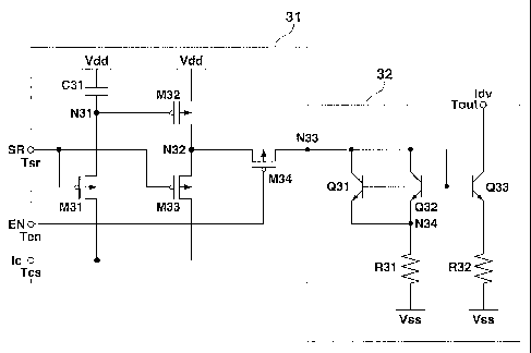
20 For example, as shown in FIG. 3, the voltage
component holding portion 31 comprises: a PMOS
transistor M31 having a source connected to a junction
N31, a drain connected to an output terminal Tcs of the
current generation circuit 10A and a gate connected to
25 a shift output terminal Tsr of the shift register; a
PMOS transistor M32 having a source and a drain
respectively connected to a high-potential power supply
CA 02462134 2004-03-26
WO 2004/003877 PCT/JP2003/008153
26
Vdd and a junction N32 and a gate connected to the
junction N31; a PMOS transistor M33 having a source and
a drain respectively connected to the junction N32 and
the output terminal Tcs of the current generation
circuit 10A and a gate connected to the shift output
terminal Tsr of the shift register 20A; a storage
capacitance C31 connected between the high-potential
power supply Vdd and the junction N31; and a PMOS
transistor M34 having a source and a drain respectively
connected and the junction N32 and an output junction
N33 to the drive current generation portion 32 on the
rear stage and a gate connected to an output control
terminal Ten to which an output enable signal EN which
is supplied from a non-illustrated control portion and
controls an output state of the control current to the
drive current generation portion 32 on the rear stage
is inputted.
Here, the PMOS transistors M31 and M33 which
perform on/off operation based on the switch changeover
signal SR from the shift register 20A constitute the
above-described switch circuit 40A.
The storage capacitance C31 provided between the
high-potential power supply Vdd and the junction N31
may be a parasitic capacitance between the gate and the
source of the PMOS transistor M32.
For example, as shown in FIG. 3, the above-
described drive current generation portion 32
CA 02462134 2004-03-26
WO 2004/003877 PCT/JP2003/008153
27
comprises: npn transistors Q31 and Q32 constituted by
the current mirror circuit, each of which has a
collector and a base connected to an output'junction
N33 of the voltage component holding 31 and an emitter
connected to a junction N34; a resistance R31 connected
between the junction N34 and a low-potential power
supply Vss; an npn transistor Q33 having a collector
connected to an output terminal Tout from which an
output current (drive current Idv) is outputted and a
base connected to the output junction N33 of the
voltage component holding 31; and a resistance R32
connected between the emitter of the npn transistor Q33
and the low-potential power supply Vss.
Here, the output current (drive current Idv) has a
current value corresponding to a predetermined current
ratio stipulated by the current mirror circuit
configuration with respect to a current value of the
control current outputted from the voltage component
holding portion 31 and inputted through the output
junction N33. In this embodiment, by supply the output
current having the negative polarity to the output
terminal Tout (load LD) (that is, by setting the
current flow direction of the drive current Idv to a
direction of the low-potential power supply Vss from
the output terminal Tout side), the current component
flows down so as to be pulled in the direction of the
current storage circuit 30A from the load LD side.
CA 02462134 2004-03-26
WO 2004/003877 PCT/JP2003/008153
28
In the current storage circuit 30A illustrated in
this embodiment, a current value of the control current
outputted from the voltage component holding portion 31
is set larger than a current value of the output
current generated by the current mirror circuit of the
drive current generation portion 32. The current value
of the control current is reduced by the current mirror
circuit with a predetermined ratio in order to
stipulate the current value of the output current.
That is, by setting the current value processed inside
the voltage component holding 31 larger than the
current value of the drive current Idv, it is possible
to increase a processing speed concerning the fetch
holding (storage) and the output operation of the
operating current Ic in the voltage component holding
31 of the current storage circuit 30A.
In the circuit configuration shown in FIG. 3, by
applying a circuit configuration which stipulates the
current ratio by using only an area ratio of the npn
transistors Q31 to Q33 in place of the resistors R31
and R32 which are connected to the emitters of the npn
transistors Q31 to Q33 constituting the current mirror
circuit of the drive current generation circuit 32 and
stipulate the current ratio in the current mirror
circuit configuration, i.e., by eliminating the
resistances R31 and R32, it is possible to suppress
occurrence of irregularities in the current components
CA 02462134 2004-03-26
WO 2004/003877 PCT/JP2003/008153
29
within the circuit caused to due to the resistances R31
and R32, and irregularities in the output current
(drive current Idv) can be greatly restrained.
As to the basic operation in the current storage
circuit (including the switch circuit) having such a
structure, the current storage operation and the
current output operation are executed with respect to
the drive cycle of the load with a predetermined timing
by which overlap in time is not generated. Each
operation will now be described hereinafter.
(Current Storage Operation)
In the current storage operation, as shown in
FIG. 4A, the PMOS transistor M34 as the output control
circuit performs the off operation by applying a
high-level output enable signal EN from the control
portion through the output control terminal Ten. In
this state, the operating currents Ic having the
current component with negative polarity corresponding
to the input signals IN1 to IN6 used to control the
drive states of the loads are supplied from the current
generation circuit 10A through the input terminal Tcs
(output terminal Tcs of the current generation circuit
10A), and the low-level switch changeover signal SR is
applied with a predetermined timing from the shift
register 20A through the shift output terminal Tsr. As
a result, the PMOS transistors M31 and M33 as the input
control circuits (switch circuits 40A) perform the on
CA 02462134 2004-03-26
WO 2004/003877 PCT/JP2003/008153
operation.
Consequently, the voltage level as the low level
corresponding to the operating currents Ic with the
negative polarity is applied to the junction N31
5 (namely, the gate terminal of the PMOS transistor M32
and one end of the storage capacitance C31), and a
potential difference is generated between the high-
potential power supply Vdd and the junction N31
(between the gate and the source of the PMOS transistor
10 M32). As a result, the PMOS transistor M32 carries out
the on operation, a write current Iw equivalent to the
operating current Ic flows down so as to be pulled in a
direction of the input terminal Tcs through the PMOS
transistors M32 and M33 from the high-potential power
15 supply.
At this moment, the electric charges corresponding
to the potential difference generated between the high-
potential power supply Vdd and the junction N31, i.e.,
between the gate and the source of the PMOS transistor
20 M32 are stored in the storage capacitance C31, and the
electric charges are held as a voltage component
corresponding to the operating current Ic. Here, to
the electric charges stored in the storage capacitance
C31 are held even after pulling of the write current Iw
25 is stopped by applying the high-level switch changeover
signal SR from the shift register 20A through the shift
output terminal Tsr upon completion of the current
CA 02462134 2004-03-26
WO 2004/003877 PCT/JP2003/008153
31
storage operation to the PMOS transistors M31 and M33
which perform the off operation.
(Current Output Operation)
Subsequently, in the load drive operation after
termination of the current storage operation, as shown
in FIG. 4B, the PMOS transistor M34 performs the on
operation by applying the output enable signal EN on
the low level from the control portion through the
output control terminal Ten. At this moment, since the
potential difference equivalent to that in the current
storage operation is generated between the gate and the
source of the PMOS transistor M32 by the voltage
component held in the storage capacitance C31, a drive
control current Iac having a current value equivalent
to that of the write current Iw (= the operating
current Ic) flows down in a direction of the output
junction N33 (current mirror circuit portion 32) from
the high-potential power supply through the PMOS
transistors M32 and M34.
As a result, the drive control current Iac
inputted to the current mirror circuit portion 32 is
converted into a drive current Idv having a current
value corresponding to a predetermined current ratio
stipulated by the current mirror circuit configuration,
and supplied to each load LD through each output
terminal Tout. Here, to the drive current Idv supplied
from each current storage circuit 30A to each load LD
CA 02462134 2004-03-26
WO 2004/003877 PCT/JP2003/008153
32
is applied the high-level output enable signal EN from
the control portion through the output control terminal
Ten upon completion of the current output operation,
and supply is stopped when the PMOS transistor M34
carries out the off operation.
(Drive Method of Current Drive Apparatus)
In the current drive apparatus having the above-
described structure, in a current write period, the
operating current Ic having a predetermined current
value according to the drive state of each load is
sequentially generated and outputted by the single
current generation circuit 10A, and the switch
changeover signal SR sequentially outputted from the
shift register 20A is sequentially applied to the
switch circuits 40A provided in accordance with the
respective output terminals Tout in synchronization
with the output timing of the operating current Ic. As
a result, the switch circuits 40A sequentially perform
the on operation with different timings synchronized
with the output timing of the operating current Ic.
The write current Iw corresponding to the operating
current Ic outputted from the current generation
circuit 10A sequentially flows down and is written in
the current storage circuits 30A, and held as the
voltage component (the above-described current storage
operation). Sequentially, in the current output
period, output of the switch changeover signal SR from
CA 02462134 2004-03-26
WO 2004/003877 PCT/JP2003/008153
33
the shift register 20A in the current write period is
terminated, all the switch circuits 40A perform the off
operation, and the operating current Ic according to
the drive states of the loads is held in all the
current storage circuits 30A. Thereafter, the output
enable signal EN is applied to the respective current
storage circuits 30A from the control portion in common
with the same timing. As a result, the currents
according to the voltage component held in the current
storage circuits 30A are simultaneously supplied as the
drive currents Idv to the loads through the output
terminals Tout (the above-described current output
operation).
By repeatedly setting such a current write period
and current output period in accordance with a
predetermined operating cycle, the loads can be caused
to operate with a predetermined drive cycle.
Therefore, according to the current drive
apparatus of this embodiment, the current storage
circuits are individually provided to the single
current generation circuit so as to correspond to a
plurality of the output terminals, the current having a
predetermined current value concerning the drive
control over the loads is generated by the current
generation circuit, and this current is sequentially
stored in each current storage circuit with a
predetermined timing. Then, the operating current
CA 02462134 2004-03-26
WO 2004/003877 PCT/JP2003/008153
34
supplied from the single current generation circuits
can be held in accordance with respective output
terminals by outputting the currents to the respective
loads from the respective current storage circuits
through the respective output terminals at the same
time, and the drive current for each output terminal
can be set based on the operating current. Therefore,
the drive currents in which irregularities between the
respective output terminals are suppressed can be
supplied, thereby driving the respective loads with the
uniform operating characteristic.
The element structure of the bipolar transistor or
the MOS transistor applied to the current drive
apparatus illustrated in this embodiment is not
restricted, and it may be appropriately subjected to
design change in accordance with the element
characteristic, a manufacturing technique, a product
cost and others.
Specifically, by sequentially repeating in
accordance with each row the operation to supply the
light emitting drive currents (drive currents) which
have the uniform current characteristic and correspond
to each display data from the individual current
storage circuits to the light emitting elements (loads)
each provided in accordance with each of the display
pixels constituting the later-described display panel
(see FIG. 15), it is possible to write the display data
CA 02462134 2004-03-26
WO 2004/003877 PCT/JP2003/008153
for one screen of the display panel into each display
pixel and causes the light emitting operation with a
predetermined brightness gradation, thereby enabling
excellent display of desired image information while
5 suppressing generation of display irregularities.
Here, the element structure of the bipolar
transistor or the MOS transistor constituting the
current storage circuit according to this embodiment is
not particularly restricted, and it may be appropri-
10 ately subjected to design change in accordance with the
element characteristic, the product technique, the
product cost and others. In particular, in the MOS
transistor constituting the voltage component holding
element, in order to obtain necessary operating speed,
15 preferably, as described below, it is possible to
excellently apply a transistor having the mobility e
of the MOS transistor being approximately 200 cm2/Vs or
a larger value.
FIG. 5A shows an equivalent circuit of a structure
20 when the electric charges are stored in the capacitance
between the gate and the source of the transistor, and
FIG. 5B is a graph showing an aged change in voltage of
the capacitance when the electric charges are stored in
the capacitance between the gate and the source of the
25 transistor.
FIG. 5A corresponds to an equivalent circuit when
predetermined electric charges are stored in the
CA 02462134 2004-03-26
WO 2004/003877 PCT/JP2003/008153
36
storage capacitance C31 in the voltage component
holding portion 31 of the current storage circuit shown
in FIG. 3, and corresponds to a case that the PMOS
transistors M32 and M33 are ON and in the conductive
state and the PMOS transistor M34 is OFF and in the
open state. Here, the transistor M corresponds to the
PMOS transistor M32, and the capacitance C corresponds
to the storage capacitance C31 which is a sum total of
a wiring capacitance, a storage capacitance and a gate
capacitance of the transistor M. For the brief
explanation, it is determined that the source S of
the transistor M and one end of the capacitance C are
set to a ground potential. FIG. 5B corresponds to a
change of a time t relative to a drain voltage V(t) of
the transistor M32, i.e., the voltage of the
capacitance C31.
Here, as shown in FIG. 5A, when a current Iin is
supplied to a drain D of the transistor M from a
constant current source, assuming that V(t) is a drain
voltage and Id is a drain current of the transistor M,
the drain current Id can be represented by the
following expression (1).
Id = A*V (t) 2 . . . (1)
wherein A=(1/2)*Cin* e*(W/L), Cin is a gate
capacitance per unit area of the transistor M, e is
the mobility of the transistor M, W is a channel width
of the transistor M, and L is a channel length. Based
CA 02462134 2004-03-26
WO 2004/003877 PCT/JP2003/008153
37
on this, a differential equation of the following
expression (2) can be established.
C*dV (t) /dt + AV (t) 2 = Iin . . . (2)
wherein the capacitance C is a sum total of the wiring
capacitance, the storage capacitance, and the gate
capacitance of the transistor M as described above. A
change of the time t relative to the drain voltage V(t)
of the transistor M, i.e., the voltage of the
capacitance C obtained by solving the above expression
is substantially as shown in FIG. 5B. Here, ti is a
time constant, and it can be represented by the
following expression (3) if the gate capacitance in the
capacitance C is larger than any other capacitance.
Further, with the time t= 3ti, the voltage V(t) reaches
a value which is 99.5% of a saturation voltage V(s).
ti = C/4A*Iin ... (3)
That is, the time constant ti is in proportion to a
value of the capacitance C and in inverse proportion to
the 1/2-th power of the mobility e.
Here, assuming that a polysilicon TFT is used as
the transistor M, the capacitance C is 6 pF, W/L is
100 m/30 m, the mobility e is 70 m2/Vs, a film
thickness of a gate insulating film is 105 nm and an
application current Iin is 10 A, a time constant T
becomes 1.42 sec. Therefore, when the number of the
scanning lines in the display panel to be driven is set
to as 120, a selection period per scanning line is
CA 02462134 2004-03-26
WO 2004/003877 PCT/JP2003/008153
38
approximately 139 sec and the number of the data lines
in which data can be written within this time is
approximately 32.
In relation to this, when the mobility e of the
transistor M is 245 m2/Vs under the above-described
condition, the time constant ti is approximately
0.096 sec. As a result, the number of the data lines
in which data can be written within the selection
period per scanning line in the display panel is
approximately 482, and a 1/4 VGA panel having the 120
scanning lines and the 160 (X RGB) data lines can be
driven.
Alternatively, if the capacitance C is 0.51 pF
even though the mobility e remains as 70 m2/Vs,
the time constant z likewise becomes approximately
0.096 sec, and the 1/4 VGA panel can be driven like
the above.
That is, in order to drive at least the 1/4 VGA
panel, the mobility e of the transistor M must have a
value of approximately 200 cm2/Vs or a larger value, or
the capacitance C must have a value smaller than
approximately 0.5 pF.
As described above, since the time constant ti is
in proportion to a value of the capacitance C and in
inverse proportion to the 1/2-th power of the mobility
e of the transistor, the time constant T can be
further decreased when the capacitance C is further
CA 02462134 2004-03-26
WO 2004/003877 PCT/JP2003/008153
39
reduced or the mobility e is further increased,
thereby driving the higher-definition display panel.
Although the structure of the transistor realizing
the mobility or the capacitance value is not particu-
larly restricted, for example, a polysilicon MOS
transistor having a continuous grain boundary formed on
an insulating substrate or an MOS transistor formed on
a monocrystal silicon substrate can satisfy the above
conditions, and it can be preferably used.
<Second Embodiment of Current Drive Apparatus>
FIG. 6 is a primary structural view showing a
second embodiment of a current drive apparatus
according to the present invention. Here, the same or
equivalent reference numerals denote structures
equivalent to those in the above-described first
embodiment, thereby simplifying or eliminating their
explanation.
The current drive apparatus according to the
second embodiment includes a pair of current storage
sections in accordance with an output terminal to which
a load is connected, and is constituted to execute in
parallel an operation to sequentially fetch a current
having a predetermined current value supplied from a
single current generation circuit by the current
storage section on one side and hold a corresponding
voltage component and operation to simultaneously
output the current based on the voltage component which
CA 02462134 2004-03-26
WO 2004/003877 PCT/JP2003/008153
has been already held in the current storage section
on the other side through the output terminal.
As shown in FIG. 6, the current drive apparatus
according to this embodiment comprises: a single
5 current generation circuit 10B which sequentially
generates and outputs an operating current Ic having a
predetermined value according to a drive stage of the
load; a plurality of current storage circuits 30B each
including a pair of current storage sections 31a and
10 31b which are provided as a pair in accordance with
each output terminal Tout in parallel, alternately
(selectively) fetch the operating current Ic supplied
from the current generation circuit lOB with individual
timings and hold a corresponding voltage component; a
15 shift register 20B (shift register sections 21a and
21b) which is provided as a pair in accordance with the
current storage sections 31a and 31b constituting the
current storage circuit 30B and sets a timing when
supplying the operating current Ic fed from the current
20 generation circuit 10B to each of the current storage
sections 31a and 31b; a plurality of input side switch
circuits 40B having switches 41a and 41b which are
provided as a pair in accordance with the current
storage sections 31a and 31b constituting the current
25 storage circuit 30B and control a supply state of the
operating current Ic from the current generation
circuit 10B to each current storage circuit 30B based
CA 02462134 2004-03-26
WO 2004/003877 PCT/JP2003/008153
41
on individual timings set by the respective shift
register sections 21a and 21b; and a plurality of
output side switch circuits 50B each of which is
provided in accordance with each output terminal Tout,
selects any of the current storage sections 31a and 31b
based on a predetermined output selection signal SEL
and controls an output stage of the current held in the
current storage sections 31a and 31b to each output
terminal Tout.
It is determined that the current generation
circuit 10B, the shift register 20B (shift register
sections 21a and 21b), the current storage circuit 30B
(current storage sections 31a and 32b) and the input
side switch circuit 40B (switches 41a and 41b) have the
structures equivalent to those in the above-described
first embodiment, thereby eliminating the detailed
explanation.
Here, the first shift register section 21a
sequentially outputs a shift output as a switch
changeover signal SR1 with a predetermined timing to
the first switch 41a provided in accordance with the
first current storage section 31a in the current
storage circuit 30B provided in accordance with each
output terminal Tout. On the other hand, the second
shift register section 21b sequentially outputs a shift
output as a switch changeover signal SR2 with a timing
which does not overlap the timing of the shift output
CA 02462134 2004-03-26
WO 2004/003877 PCT/JP2003/008153
42
from the shift register section 21a in time to the
second switch 41b provided in accordance with the
second current storage section 31b in the current
storage circuit 30B provided in accordance with each
output terminal Tout.
Furthermore, the output side switch circuit 50B is
synchronized with the output timings of the switch
changeover signals SR1 and SR2 from the shift register
sections 21a and 21b based on an output selection
signal SEL outputted from a non-illustrated control
portion, and operates so as to select the current
storage section (non-selected current storage section
side) of the switch which is not performing the on
operation in the input side switch circuit 40B.
In the current drive apparatus having such a
structure, in a first operation period (a current write
period on the first current storage section 31a side/a
current output period on the second current storage
section 31b side), when the switch changeover signal
SR1 from the first shift register section 21a is
sequentially outputted to each switch 41a provided in
accordance with the current storage section 31a of each
current storage circuit 30B, each switch 41a sequen-
tially effects the on operation only in a predetermined
period, and electric charges corresponding to an
operating current Ic supplied from the current
generation circuit lOB are sequentially written in each
CA 02462134 2004-03-26
WO 2004/003877 PCT/JP2003/008153
43
current storage section 31a as a voltage component. At
this moment, the switch changeover signal SR2 is not
outputted from the second shift register section 21b,
and all the switches 41b are in the off state.
Moreover, at this moment, the output selection
signal SEL which changes over and sets the output side
switch circuit 50B provided in accordance with each
output terminal Tout to the current storage section 31b
side is outputted in common, and an output enable
signal EN2 is outputted to all the current storage
sections 31b with a predetermined timing in common. As
a result, a current based on the electric charges which
have been already held in each current storage section
31b is simultaneously outputted as a drive current Idv
to each load through each output terminal Tout with the
same timing.
Subsequently, in a second operation period (a
current output period on the first current storage
section 31a side/a current write period on the second
current storage section 31b side) set after termination
of the fist operation period, when the switch
changeover signal SR2 from the second shift register
section 21b is sequentially outputted to each switch
41b provided in accordance with the current storage
section 31b of each current storage circuit 30B, each
switch 41b sequentially performs the on operation only
in a predetermined period, and electric charges
CA 02462134 2004-03-26
WO 2004/003877 PCT/JP2003/008153
44
corresponding to the operating current Ic supplied from
the current generation circuit lOB are sequentially
written in each current storage section 31b as a
voltage component. At this moment, the switch
changeover signal SR1 is not outputted from the shift
register section 21a, and all the switches 41a are in
the off state.
Additionally, at this moment, the output selection
signal SEL used to change over and set the output side
switch circuit 50B to the current storage section 31a
side is outputted from the control portion in common,
and the output enable signal EN1 is outputted to all
the current storage sections 31a with a predetermined
timing in common. As a result, a current based on the
electric charges held in each current storage section
31a in the first operation period is simultaneously
outputted as the drive current Idv to each load through
each output terminal Tout with the same timing.
By controlling such a first and second operation
period so as to be repeated in accordance with a
predetermined operation cycle, the operation to hold
the electric charges corresponding to the operating
current Ic outputted from the current generation
circuit 10B in one of a pair of the current storage
sections 31a and 31b, and the operation to output the
current based on the electric charges held in the other
current storage section as the drive current Idv are
CA 02462134 2004-03-26
WO 2004/003877 PCT/JP2003/008153
alternately executed in parallel.
Therefore, according to the current drive
apparatus of this embodiment, like the above-described
first embodiment, the operating current outputted from
5 the single current generation circuit is sequentially
fetched and held in each current storage circuit
(current storage section), and outputted with a
predetermined timing at the same time. As a result,
the current with the uniform current characteristic
10 supplied from the single current source can be held in
accordance with each output terminal, and irregulari-
ties in the drive current between the respective output
terminals can be suppressed. Further, a pair of the
current storage sections are provided in accordance
15 with each output terminal, and the operation to
sequentially write the electric charges corresponding
to the current outputted from the current generation
circuit on one current storage section side and the
operation to simultaneously output the current based on
20 the electric charges held on the other current storage
section side are executed in parallel. As a result,
the waiting time for the current write operation to the
current storage section can be reduced or eliminated,
the supply time of the drive current to each load can
25 be extended, and the drive state of each load can be
finely controlled. Furthermore, the time to fetch the
operating current into each current storage section and
CA 02462134 2004-03-26
WO 2004/003877 PCT/JP2003/008153
46
hold it can be prolonged, thereby stably carrying out
the holding operation in the current storage section.
<Third Embodiment of Current Drive Apparatus>
FIG. 7 is a primary structural view showing a
third embodiment of a current drive apparatus according
to the present invention. Here, the same or equivalent
reference numerals denote the structures equivalent to
those in the first and second embodiments, thereby
simplifying or eliminating their explanation.
The current drive apparatus according to the third
embodiment has current storage sections on two stages
provided in series in accordance with each output
terminal to which a load is connected, and is
constituted so as to execute an operation to sequen-
tially hold a current having a predetermined current
value supplied from a single current generation circuit
by the current storage section on the front stage*and
an operation to hold the current supplied from the
current storage section on the front stage by the
current storage section on the rear stage and then
collectively outputs it through the output terminal.
As shown in FIG. 7, the current drive apparatus
according to this embodiment comprises: a single
current generation circuit 10C which sequentially
generates and outputs an operating current Ic having a
predetermined current value according to a drive state
of the load; a plurality of current storage circuits
CA 02462134 2004-03-26
WO 2004/003877 PCT/JP2003/008153
47
30C each including a current storage section 32a on a
front stage and a current storage section 32b on a rear
stage provided in series in accordance with each output
terminal Tout; a shift register 20C which sets a timing
when supplying the operating current Ic fed from the
current generation circuit 10C to the current storage
section 32a on the front stage; and switch circuits 40C
each of which controls a supply state of the operating
current Ic from the current generation circuit 10C to
each current storage circuit 30C. It is to be noted
that the current generation circuit 10C, the shift
register 20C, the current storage circuit 30C (current
storage sections 32a and 32b) and the switch circuit
40C applied to this embodiment have the structures
equivalent to, e.g., those in the above-described first
embodiment, thereby eliminating their detailed
explanation.
In each current storage circuit 30C, the operating
current Ic supplied from the current generation circuit
10B is fetched into the current storage section 32a
with a predetermined timing, a corresponding voltage
component is held, and a current based on the held
voltage component is supplied to the current storage
section 32b on the rear stage with a predetermined
timing based on a first output enable signal EN1 fed
from a non-illustrated control portion or circuit. At
this moment, the current storage section 32b on the
CA 02462134 2004-03-26
WO 2004/003877 PCT/JP2003/008153
48
rear stage fetches the current fed from the current
storage section 32a on the front stage, holds a
corresponding voltage component, and outputs a current
based on the held voltage component through the output
terminal Tout based on a second enable signal EN2 fed
from the control portion.
In the current drive apparatus having such a
structure, in a first operation period, a switch
changeover signal SR from the shift register 20C is
sequentially outputted to the switch circuit 40C
provided in accordance with each current storage
circuit 30C. As a result, the switch circuit 40C
sequentially performs the on operation only in a
predetermined period, and electric charges (voltage
component) corresponding to an operating current Ic
supplied from the current generation circuit lOC is
sequentially written in the current storage section
32a on the front stage.
Furthermore, at this moment, when the second
output enable signal EN2 is outputted from the control
portion to all the current storage sections 32b on the
rear stages in common with a predetermined timing, a
current based on the electric charges which have been
already held in each current storage section 32b is
simultaneously outputted as a drive current Idv to each
load through each output terminal Tout with the same
timing.
CA 02462134 2004-03-26
WO 2004/003877 PCT/JP2003/008153
49
Then, with a predetermined timing after completion
of the first operation period, the first output enable
signal EN1 is outputted from the control portion to all
the current storage sections 32a on the front stage in
common. As a result, the current held in each current
storage section 32a in the first operation period is
collectively supplied to the current storage section
32b on the rear stage and held (supply operation
period).
Subsequently, in a second operation period set
after completion of the supply operation of the current
to the rear stage in the current storage circuit 30C,
like the above-described first operation period, the
switch changeover signal SR from the shift register 20C
is again sequentially outputted to each switch circuit
40C. Consequently, the operating current Ic supplied
from the current generation circuit 10C is sequentially
written in the current storage section 32a on the front
stage and, at this moment, the second output enable
signal EN2 is outputted to the current storage section
32b on the rear stage in common with a predetermined
timing. As a result, the current supplied from and
held in each current storage section 32b is
simultaneously outputted to each load as the drive
current Idv.
By controlling such a series of operation periods
so as to be repeated in accordance with a predetermined
CA 02462134 2004-03-26
WO 2004/003877 PCT/JP2003/008153
operation cycle, the operation to hold the electric
charges corresponding to the operating current Ic
outputted from the current generation circuit lOC in
the current storage section 32a on the front stage, and
5 the operation to output the current based on the
current fed from the current storage section 32a on the
front stage and supplied therefrom, from the current
storage section 32b on the rear stage as the drive
current Idv are executed in parallel.
10 Therefore, according to the current drive
apparatus of this embodiment, like the above-described
first embodiment, since the drive current of each
output terminal is set based on the operating current
fed from the single current generation circuit,
15 irregularities in the drive current between the
respective output terminals can be suppressed.
Moreover, like the above-described second embodiment,
the supply time of the drive current to each load can
be prolonged, and the drive state of each load can be
20 finely controlled. Additionally, the time to fetch the
current into each current storage section and hold it
can be extended, thereby stably executing the holding
operation in the current storage section.
<Fourth Embodiment of Current Drive Apparatus>
25 FIG. 8 is a primary structural view showing a
fourth embodiment of a current drive apparatus
according to the present invention. Here, the same or
CA 02462134 2004-03-26
WO 2004/003877 PCT/JP2003/008153
51
equivalent reference numerals denote structures
equivalent to those in the first to third embodiments
mentioned above, thereby simplifying or eliminating
their explanation.
In the structure described in conjunction with the
first to third embodiments mentioned above, the current
drive apparatus according to the fourth embodiment
determines as one group a structure including the
predetermined number of output terminals, current
storage circuits provided in accordance with the output
terminals, a shift register and switch circuits, forms
each group on an individual semiconductor chip,
provides a single current generation circuit with
respect to each group (semiconductor chip), and
supplies a current having a predetermined current value
in common. It is to be noted that, in the following
concrete example, although description will be given as
to the case where the present invention is applied to
the structure explained in conjunction with the second
embodiment, but it can be similarly applied to any
other embodiment.
As shown in FIG. 8, the current drive apparatus
according to this embodiment comprises: a predetermined
number of output terminals Tout equivalent to, e.g.,
the structure described in conjunction with the second
embodiment (see FIG. 6); a plurality of current storage
circuits 30D (current storage sections 33a and 33b)
CA 02462134 2004-03-26
WO 2004/003877 PCT/JP2003/008153
52
provided in accordance with the output terminals Tout;
a shift register 20D (shift register sections 23a and
23b); a plurality of input side switch circuits 40D
(switches 43a and 43b); a plurality of semiconductor
chips CP1, CP2, ===, CPn on which circuit configurations
having a plurality of output side switch circuits 50D
are respectively formed; and a single current
generation circuit 10D which sequentially generates an
operating current Ic having a predetermined current
value according to a drive stage of a load connected to
each output terminal Tout with respect to each of the
semiconductor chips CP1, CP2, ===, CPn and supplies it
in common. Here, the current generation circuit 10D,
the shift register 20D (shift register sections 23a and
23b), the current storage circuit 30D (current storage
sections 33a and 33b), the current storage circuit 30D
(current storage sections 33a and 33b), the input side
switch circuit 40D (switches 43a and 43b) and the
output side switch circuit 50D have the structures
equivalent to, e.g., those in the second embodiment
mentioned above, thereby eliminating their detailed
explanation.
Here, the current generation circuit 10D may be
formed on a specific semiconductor chip among a
plurality of the semiconductor chips CP1, CP2, === CPn
each having a circuit configuration including the
current storage circuit 30D formed thereto.
CA 02462134 2004-03-26
WO 2004/003877 PCT/JP2003/008153
53
Alternatively, the same circuit may be formed on each
of the semiconductor chips CP1, CP2, === CPn, and any
one of them may be used to cause other semiconductor
chips to enter non-operating state or to be bypassed.
Further, the current generation circuit 10D may be
formed on a semiconductor chip different from a
plurality of the semiconductor chips CP1, CP2, === CPn.
It is good enough that each of the semiconductor
chips CP1, CP2, === CPn applied to this embodiment is
formed of a semiconductor material such as single
crystal silicone, and its material is not restricted in
particular.
In the current drive apparatus having such a
structure, by executing the operation similar to that
of the above-described second embodiment, the operating
current Ic outputted from the current generation
circuit 10D is supplied to the respective semiconductor
chips CP1, CP2, === CPn in common, it is sequentially
fetched into one of a pair of the current storage
sections 33a and 33b in the current storage circuit 30D
provided in accordance with each of the semiconductor
chips CP1, CP2, ==- CPn, and a corresponding voltage
component is held. Furthermore, a current based on the
voltage component held in the other current storage
section is simultaneously outputted to the corre-
sponding load through the output terminal Tout of each
of the respective semiconductor chips CP1, CP2, === CPn.
CA 02462134 2004-03-26
WO 2004/003877 PCT/JP2003/008153
54
These operations are alternately and continuously
executed.
Therefore, according to the current drive
apparatus of this embodiment, only the single current
generation circuit is provided with respect to
semiconductor chips, and individual current circuits
are not provided in accordance with the respective
semiconductor chips. Accordingly, the circuit
configuration formed on each semiconductor chip can be
simplified, and the number of terminals can be reduced,
thereby achieving minimization of the apparatus scale
or decrease in the product cost. Moreover, even if a
plurality of semiconductor chips are provided in
accordance with the number of the output terminals
connected to the loads, since the current having the
uniform current characteristic supplied from the single
current source can be held in the current storage
circuit in each semiconductor chip, irregularities in
the drive current between the respective output
terminals and between the respective semiconductor
chips can be suppressed, thereby driving each load with
the uniform operation characteristic.
Specifically, in the later-described display panel
(see FIG. 15), even if the number of display pixels is
increased in order to realize the high definition of
the display image quality and/or a large screen of the
display panel and the data driver is constituted by a
CA 02462134 2004-03-26
WO 2004/003877 PCT/JP2003/008153
plurality of driver chips (semiconductor chips), by
sequentially repeating for each row the operation to
sequentially supply a predetermined current according
to display data outputted from the single current
5 generation circuit to the current storage circuit
formed on each driver chip and simultaneously supply
the light emitting drive current (drive current) to
each light emitting element with a predetermined
timing, the display data for one screen of the display
10 panel can be written in each display pixel and the
light emitting operation can be performed with a
predetermined brightness gradation. Therefore, image
information of the high-definition and large-screen
size can be excellently display while suppressing
15 occurrence of display irregularities.
<Fifth Embodiment of Current Drive Apparatus>
FIG. 9 is a primary structural view showing a
fifth embodiment of a current drive apparatus according
to the present invention. Here, the same or equivalent
20 reference numerals denote structures equivalent to
those in the first to fourth embodiments mentioned
above, thereby simplifying or eliminating their
explanation.
The current drive apparatus according to this
25 embodiment can be preferably applied to driving of,
e.g., a simple matrix type display panel (see FIG. 2),
and this can be applied to a drive mode which displays
CA 02462134 2004-03-26
WO 2004/003877 PCT/JP2003/008153
56
a desired image by performing a pulse width modulation
(PWM) drive mode by supplying a current having a fixed
current and set to a supply time (pulse width)
according to display data from each output terminal to
each display element (load).
The current drive apparatus according to this
embodiment have a plurality of semiconductor chips,
comprises a circuit configuration which is the same as
one group including, e.g., the predetermined number of
output terminals, current storage circuits provided in
accordance with the output terminals, a shift register
and switch circuits described according to the fourth
embodiment, and has a structure that each single input
current storage circuit is provided to an input portion
of this circuit configuration. As a result, the
operation to fetch a fixed current into the current
storage circuit for each output terminal on the
semiconductor chip can be simultaneously performed on
the respectively semiconductor chips in parallel. In
the following concrete example, although description
will be given as to the case that the present invention
is applied to a structure described in connection with
the fourth embodiment, it can be likewise applied to
any other embodiment.
As shown in FIG. 9, the current drive apparatus
according to this embodiment includes a circuit
configuration which is equivalent to, e.g., the
CA 02462134 2004-03-26
WO 2004/003877 PCT/JP2003/008153
57
structure described in conjunction with the fourth
embodiment and have the predetermined number of output
terminals Tout, a plurality of current storage circuits
30E (current storage sections 34a and 34b) provided in
accordance with the output terminals Tout, a shift
register 20E (shift register sections 24a and 24b), a
plurality of input side switch circuits 40E (switches
44a and 44b), and a plurality of output side switch
circuits 50E. Furthermore, this apparatus comprises: a
plurality of semiconductor chips CP1, CP2, === CPn each
having an input switch circuit 60E which performs the
on/off operation based on a shift output (switch
changeover signal) from a non-illustrated shift
register or control portion being formed thereon on a
front stage of the circuit configuration, i.e., at an
input portion to which the operating current Ic
outputted from the current generation circuit 10E is
supplied and an input current storage circuit 70E which
fetches and holds an operating current Ic outputted
from a current generation circuit 10E; and the single
current generation circuit 10E which supplies the
predetermined operating current Ic to the respective
semiconductor chips CP1, CP2, === CPn in common.
The current generation circuit 10E, the shift
register 20E (shift register sections 24a and 24b), the
current storage circuit 30E (current storage sections
34a and 34b), the input side switch circuit 40E
CA 02462134 2004-03-26
WO 2004/003877 PCT/JP2003/008153
58
(switches 44a and 44b) and the output side switch
circuit 50E applied to this embodiment have the
structures equivalent to those in the fourth embodiment
mentioned above, thereby eliminating the detailed
description.
Here, the input switch circuit 60E provided to
each of the semiconductor switches CP1, CP2, === CPn
performs the on operation based on a shift output
(switch changeover signal) sequentially outputted from
a non-illustrated shift register (or a control
portion), sets the operating current Ic outputted from
the current generation circuit l0E to the write state
in order to feed this current to each of the
semiconductor chips CP1, CP2, ==- CPn, and controls in
such a manner that the operating current Ic is fetched
into and held in the input current storage circuit 70E.
The input current storage circuit 70E has the
structure equivalent to, e.g., that of the current
storage circuit in the first embodiment mentioned
above, fetches the operating current Ic outputted from
the current generation circuit 10E with a predetermined
timing that the input switch circuit 60E enters the on
state, holds a corresponding voltage component, and
outputs the operating current Ic based on the held
voltage component to the current storage circuit 30E
(any one of the current storage sections 34a and 34b)
through the input side switch circuit 40E (any one of
CA 02462134 2004-03-26
WO 2004/003877 PCT/JP2003/008153
59
the switches 44a and 44b) in each semiconductor chip
based on an output enable signal outputted from a non-
illustrated control portion.
In the current drive apparatus having such a
structure, the operating current Ic having a
predetermined current value outputted from the current
generation circuit l0E is supplied to each of the
semiconductor chips CP1, CP2, === CPn in common, it is
sequentially fetched into the input current storage
circuit 70E through the input switch circuit 60E
provided in accordance with each of the semiconductor
chips CP1, CP2, === CPn with a predetermined timing, and
a corresponding voltage component is held.
In a first operation period, a current based on
the voltage component held in the input current storage
circuit 70E is supplied to one storage section of the
current storage circuit 30E (e.g., the first current
storage section 34a) through one switch in the input
side switch circuit 40E in common (e.g., the first
switch 44a) in each of the semiconductor chips CP1,
CP2, -== CPn, and a corresponding voltage component is
held. At this moment, a current based on the voltage
component which has been already held in the other one
storage section in the current storage circuit 30E
(e.g., the second current storage section 34b) is
simultaneously outputted as a drive current Idv to the
respective output terminals Tout.
CA 02462134 2004-03-26
WO 2004/003877 PCT/JP2003/008153
Subsequently, with a predetermined timing after
completion of the first operation period, the operating
current Ic outputted from the current generation
circuit 10E is again sequentially fetched into and held
5 in the input current storage circuit 70E through the
input switch circuit 60E provided in accordance with
each of the semiconductor chips CP1, CP2, === CPn with a
predetermined timing.
Then, after completion of the first operation
10 period, in a second operation period which is set after
termination of the fetching and holding operation of
the operating current Ic into the input current storage
circuit 70E, like the above-described first operation
period, the current based on the voltage component held
15 in the input current storage circuit 70E is supplied to
the other one storage section in the current storage
circuit 30E (e.g., the current storage section 34b)
through the other one switch in the input side switch
circuit 40E (e.g., the switch 44b) in each of the
20 semiconductor chips CP1, CP2, === CPn in parallel, and a
corresponding voltage component is held. Furthermore,
at this moment, the current based on the voltage
component held in one storage section in the current
storage circuit 30E (e.g., the current storage section
25 34a) in the first operation period is simultaneously
outputted to the respective output terminals Tout as a
drive current Idv.
CA 02462134 2004-03-26
WO 2004/003877 PCT/JP2003/008153
61
By repeatedly setting such a series of the
operation periods in accordance with a predetermined
operation period, the operation to sequentially hold
the operating current Ic outputted from the current
generation circuit 10C in the input current storage
circuit 70E in the input portion, supply it to the
current storage circuit 30E on the rear stage and fetch
it into one storage section in the current storage
circuit 30E and the operation to output the current
held in the other storage section as the drive current
Idv to the respective output terminals Tout at same
time are alternately and continuously executed.
Therefore, according to the current drive
apparatus of this embodiment, a current outputted from
the single current generation is sequentially fetched
into the input current storage circuit provided in
accordance with each semiconductor chip, it is then
fetched into and held in the current storage circuit on
the rear stage provided in accordance with each output
terminal in parallel in each semiconductor chip, and it
is collectively outputted with a predetermined timing.
As a result, irregularities in the drive current
between the respective output terminals can be
suppressed, and the operation to fetch the current into
the current storage circuit corresponding to the output
terminal of each semiconductor chip can be performed
between the respective semiconductor chips in parallel.
CA 02462134 2004-03-26
WO 2004/003877 PCT/JP2003/008153
62
Therefore, the time required to fetch and hold the
current in each current storage circuit can be
prolonged, thereby stably effecting the holding
operation in the current storage section.
Here, in this embodiment, the operating current Ic
fetched and held by the input current storage circuit
70E provided in accordance with each of the semi-
conductor chips CP1, CP2, -== CPn is sequentially
fetched into and held in a plurality of the current
storage circuits 30E provided in the respective
semiconductor chips CP1, CP2, === CPn, and it is
outputted from the respective output terminals Tout at
the same time with a predetermined timing. The drive
current Idv supplied to each load through each output
terminal Tout becomes a constant current having the
same current value with each timing. Further, in order
to perform driving of pulse width modulation (PWM) by
using the current drive apparatus according to this
embodiment, for example, as shown in FIG. 9, by adding
a PWM control circuit 65E by which display data IN is
supplied between each output terminal Tout and the
display element (load) and an application time of the
current to be supplied to each load is controlled in
accordance with the display data, each load can be
caused to operate by pulse width modulation (PWM).
This PWM control circuit 65E may be integrally formed
in each of the semiconductor chips CP1, CP2, === CPn, or
CA 02462134 2004-03-26
WO 2004/003877 PCT/JP2003/008153
63
it may be formed on a semiconductor chip different from
the respective semiconductor chips so as to be electri-
cally connected to the respective semiconductor chips
CP1, CP2, === CPn.
That is, in a later-described simple matrix type
display panel (see FIG. 20), by sequentially repeating
for each row the operation to supply a light emitting
drive current (drive current) having the uniform
current characteristic and consisting of a constant
current set to a supply time (pulse width) according to
each display data from all of the respective output
terminals of the driver chips (semiconductor chips)
constituting the data driver with respect to the light
emitting elements (loads) in a predetermined display
period, the display data for one screen of the display
panel can be written in each display pixel and the
light emitting operation can be performed with a
predetermined brightness gradation. Thus, desired
image information can be excellently displayed while
suppressing occurrence of display irregularities.
<Sixth Embodiment of Current Drive Apparatus>
FIG. 10 is a primary structural view showing a
sixth embodiment of a current drive apparatus according
to the present invention. Here, the same or equivalent
reference numerals denote structures equivalent to
those in the first to fifth embodiments mentioned
above, thereby simplifying or eliminating their
CA 02462134 2004-03-26
WO 2004/003877 PCT/JP2003/008153
64
explanation.
In the structure described in conjunction with the
above-described fifth embodiment, a current drive
apparatus according to the sixth embodiment has a
structure that an input current storage circuit
provided in accordance with each semiconductor chip has
a pair of current storage sections provided in
parallel. In the following concrete example, although
description will be given as to the case that the
present invention is applied to the structure described
in conjunction with the above fifth embodiment, but it
can be likewise applied to any other embodiment.
Specifically, as shown in FIG. 10, in the
structure of the fifth embodiment (see FIG. 9), the
current drive apparatus according to this embodiment
has a structure that an input current storage circuit
70F provided at an input portion of each of semi-
conductor chips CP1, CP2, === CPn includes a pair of
current storage sections 71a and 71b arranged in
parallel with each other and individual switch circuits
60F and 80F used to selectively connect one of the
current storage sections 71a and 71b are provided on
the input side and the output side of the input current
storage circuit 70F. Any other structure applied to
this embodiment has a structure equivalent to that of
the fifth embodiment mentioned above, thereby
eliminating the detailed structure.
CA 02462134 2004-03-26
WO 2004/003877 PCT/JP2003/008153
In the current drive apparatus having such a
structure, an operating current Ic outputted from the
current generation circuit 10F is supplied to the
respective semiconductor chips CP1, CP2, === CPn in
5 common, and it is applied to the switch circuits 60F
and 80F provided at the input portion of each of the
semiconductor chips CPl, CP2, === CPn. As a result, the
operation to sequentially fetch the operating current
Ic into one of a pair of the current storage sections
10 71a and 72b of the current storage circuit 70F and hold
a corresponding voltage component and the operation to
supply the operating current Ic based on the voltage
component which has been already held on the other side
to a plurality of the current storage circuits 30F on
15 the rear stages are alternately and continuously
executed in parallel.
In a plurality of the current storage circuits 30F
on the rear stages; the operation to sequentially fetch
an operating current Ic fed from the input current
20 storage circuit 70F into one of the current storage
sections 35a and 35b with a predetermined timing and
the operation to collectively output the current based
on the voltage component held on the other side through
the output terminal are alternately and continuously
25 executed in parallel.
Therefore, according to the current drive
apparatus of this embodiment, in the state that the
CA 02462134 2004-03-26
WO 2004/003877 PCT/JP2003/008153
66
current outputted from the single current generation
circuit is sequentially written into one input current
storage section of the input current storage circuit
provided in accordance with each semiconductor chip,
the current held in the other input current storage
section is supplied to, fetched into and held in the
current storage section provided in accordance with
each output terminal. Thus, the time required to fetch
and hold the current in each input current storage
section can be prolonged, and the holding operation in
the input current storage section can be stably carried
out. Further, since the waiting time of the operation
to write the current to each semiconductor chip can be
reduced or eliminated, the supply time of the drive
current to the load can be prolonged, thereby finely
controlling the drive state.
In this embodiment, like the fifth embodiment
mentioned above, the drive current Idv supplied to each
load through each output terminal Tout becomes a
constant current having the same current value with
each timing. Further, like the fifth embodiment, by
providing the PMW control circuit 60F, applying the
pulse width modulation (PWM) drive mode and adjusting
the supply time (pulse width) of the constant current
to each load, each load can be operated in a desired
drive state.
CA 02462134 2004-03-26
WO 2004/003877 PCT/JP2003/008153
67
<Seventh Embodiment of Current Drive Apparatus>
FIG. 11 is a primary structural view showing a
seventh embodiment of a current drive apparatus
according to the present invention. Here, the same or
equivalent reference numerals denote structures
equivalent to those in the first to sixth embodiments,
thereby simplifying or eliminating their explanation.
The current drive apparatus according to the
seventh embodiment has a structure that a plurality of
reference currents supplied from the single reference
current generation circuit including a plurality of
reference current generation sections which generate
and output reference currents having current values set
so as to have weightings different from each other are
individually held in a plurality of the reference
current storage sections provided in accordance with
the reference currents and predetermined currents
according to drive states of loads are sequentially
generated based on the predetermined number of digital
input signals.
As shown in FIG. 11, the current drive apparatus
according to this embodiment comprises: a reference
current generation circuit (reference current
generation circuit) 10G including four reference
current generation sections 11a to 11d which
individually generate and output reference currents I1,
12, 14 and 18 to which weightings of, e.g., 1:2:4:8 are
CA 02462134 2004-03-26
WO 2004/003877 PCT/JP2003/008153
68
set; a shift register SFR which sets a timing when
collectively supplying the respective reference
currents 11, 12, 14 and 18 fed from the reference
current generation circuit 10G to a reference current
storage circuits 90G in parallel; the current storage
circuits 90G each having a plurality of reference
current storage sections 91a to 91d which individually
fetch and hold reference currents 11, 12, 14 and 18
supplied from the reference current generation circuit
lOG; input side switch circuits SWA each of which
controls supply states of the reference currents I1,
12, I4 and 18 from the reference current generation
circuit 10G (reference current generation sections 11a
to 11d) to the reference current storage circuit 90G
based on a timing set by a switch changeover signal
(shift output) SRs outputted from the shift register
SFR with a predetermined timing; output side switch
circuits (gradation current generation circuits) SWB
each of which selects an arbitrary reference current
storage section in the reference current storage
sections 91a to 91d constituting the reference current
storage circuit 90G, combines (adds) the reference
currents held in the selected reference current storage
section and generates a current Is having a predeter-
mined current value corresponding to a drive state of a
load; a plurality of current storage circuits 30G which
are provided in accordance with each output terminal
CA 02462134 2004-03-26
WO 2004/003877 PCT/JP2003/008153
69
Tout and fetch and hold the current Is generated by the
output side switch circuit SWB with individual timings;
and a plurality of switch circuits 40G which are
provided in accordance with the current storage
circuits 30G and control a supply state of the current
Is from the output side switch circuit SWB to each
current storage circuit 30G based on a timing set by a
non-illustrated shift register (specifically, this is
equivalent to the shift register shown in FIG. 1).
In this embodiment, the structure having the
reference current generation circuit lOG, the reference
current storage circuit 90G, the input side switch
circuit SWA and the output side switch circuit SWB has
a function as a current generation circuit which
generates and outputs the current Is having a
predetermined value according to a drive state of each
load. The structure having the current storage
circuits 30G and the switch circuits 40G has a function
as a current storage circuit described in conjunction
with the foregoing embodiments.
Here, in the current drive apparatus according to
this embodiment, the structure including the predeter-
mined number of the output terminals Tout, the current
storage circuits 30G respectively provided in accordance
with the output terminals Tout, the input side switch
circuits 40G, the reference current storage circuit 90G
which generates the predetermined current Is supplied to
CA 02462134 2004-03-26
WO 2004/003877 PCT/JP2003/008153
the current storage circuits 30G and the input side and
output side switch circuits SWA and SWB is determined as
each group, and each group is formed on each of the
semiconductor chips CP1, CP2, -=- CP2. Further, the
5 single reference current generation circuit lOG is
provided with respect to the groups (semiconductor
chips) in such a manner that the reference currents I1,
12, 14 and 18 outputted from the reference current
generation circuit lOG are supplied in common.
10 The reference current generation sections 11a to
11d have the circuit structure (see FIG. 2) equivalent
to the current generation circuit described in
accordance with the foregoing embodiments, and it is
possible to apply a structure obtained by appropriately
15 designing the circuit configuration in such a manner
that a ratio of the current values of the reference
currents generated by the reference current generation
sections 11a to 11d becomes, e.g., 1:2:4:8. It is to
be noted that the shift register SFR, the reference
20 current storage circuits 90G (reference current storage
section 91a to 91d) and the input side switch circuit
SWA applied to this embodiment have the structures
equivalent to those described in conjunction with the
foregoing embodiments, thereby eliminating the detailed
25 explanation.
In the current drive apparatus having such a
structure, in a reference current generation period,
CA 02462134 2004-03-26
WO 2004/003877 PCT/JP2003/008153
71
the reference currents 11, 12, 14 and 18 to which the
current values are set so as to have the weighting of
1:2:4:8 by the reference current generation sections
11a to 11d constituting the reference current
generation circuit 10G are generated and outputted, and
a switch changeover signal SRs sequentially outputted
from the shift register SFR is sequentially applied to
each input side switch circuit SWA. As a result, the
switch circuit SWA sequentially performs the on
operation with different timings only in a predeter-
mined period, the reference currents 11, 12, 14 and 18
outputted from the reference current generation circuit
10G are simultaneously supplied to the reference
current storage sections 91a to 91d, and corresponding
voltage components are individually held in the
respective reference current storage sections.
Subsequently, in a current output period, output
of the switch changeover signal SRs from the shift
register SFR is completed, all the input side switch
circuits SWA execute the off operation, and the voltage
components corresponding to the reference currents I1,
12, 14 and 18 are held in all the reference current
storage circuits 90G. Thereafter, an output enable
signal ENs is applied to the reference current storage
sections 91a to 91d from a non-illustrated control
portion or circuit in common, and digital input signals
IN1 to IN4 are applied to the output side switch
CA 02462134 2004-03-26
WO 2004/003877 PCT/JP2003/008153
72
circuits SWB individually provided to the reference
current storage sections 91a to 91d. As a result, for
example, only the output side switch circuits SWB to
which the high-level digital input signals IN1 to IN4
are applied perform the on-operation, the reference
currents based on the held voltage components are
selectively outputted, and these reference currents are
combined (added). As a result, the currents Is having
the current values according to the signal levels of
the digital input signals IN1 to IN4 are generated.
Subsequently, in a current write period, the
switch changeover signals SR from a non-illustrated
shift register are sequentially outputted to the switch
circuits 40G. As a result, the switch circuits 40G
sequentially carry out the on operation only in a
predetermined period, the currents Is supplied from the
reference current storage circuit 90G through the
output side switch circuit SWB are sequentially
supplied and fetched into the current storage circuits
30G, and corresponding voltage components are held.
Then, in a drive current output period, the output
enable signal EN is outputted from a non-illustrated
control portion to all the current storage sections 30G
with a predetermined timing in common, currents based
on the voltage components held in the current storage
circuits 30G are simultaneously outputted as drive
currents Idv to the respective loads through the
CA 02462134 2004-03-26
WO 2004/003877 PCT/JP2003/008153
73
respective output terminals Tout with the same timing.
By repeatedly setting the reference current
generation period, the current output period, the
current write period and the drive current output
period described above in accordance with a
predetermined operation cycle, the loads can be
operated in a predetermined drive cycle.
Therefore, according to the current drive
apparatus of this embodiment, a plurality of the
reference current storage sections in which the
reference currents to which the current values are set
so as to have weightings different from each other are
arbitrarily selected based on the predetermined number
of the digital input signals, and the reference
currents held in the selected reference current storage
sections are combined. In this manner, predetermined
currents of the analog signals corresponding to the
drive states of the loads are generated, the operation
to hold the currents in the current storage circuits
provided at the respective output terminals is
sequentially executed, and the held currents are
simultaneously supplied to the respective loads as the
drive currents with a predetermined timing. As a
result, each load can be operated in the drive state
excellently corresponding to the input signal with a
relatively simple apparatus structure. Furthermore,
the reference currents having the uniform current
CA 02462134 2004-03-26
WO 2004/003877 PCT/JP2003/008153
74
characteristic outputted from the single current
generation circuit are supplied to the reference
current storage circuits provided in accordance with
each semiconductor chip in common, and the drive
currents are generated based on the reference currents.
As a result, it is possible to excellently suppress
irregularities in the drive currents between the
semiconductor chips and between the output terminals
provided to each semiconductor chip.
In this embodiment, although description has been
given as to the case where the structure described in
conjunction with the first embodiment is applied as the
current storage circuit, it is possible to apply a
structure that a plurality of the current storage
sections explained with reference to the other
embodiments are provided and the operation to
sequentially fetch and hold the currents Is supplied
from the reference current storage circuits and the
operation to simultaneously output the held currents as
the drive currents through the output terminals are
alternately executed.
Specifically, in a later-described display panel
(see FIG. 15), even if the number of the display pixels
(light emitting elements; loads) is increased in order
to realize a high definition of the display image
quality and/or a large screen of the display panel and
the data driver constructed by a plurality of the
CA 02462134 2004-03-26
WO 2004/003877 PCT/JP2003/008153
driver chips (semiconductor chips) is applied, the
reference currents outputted from the single reference
current generation circuit can be sequentially supplied
to the respective driver chips, the light emitting
5 drive currents (analog signals) having the current
values excellently corresponding to display data
(digital input signals) can be sequentially generated
based on the reference currents and simultaneously
supplied to the respective light emitting elements with
10 a predetermined timing. Therefore, it is possible to
realize the display apparatus which can excellently
suppress irregularities in the light emitting drive
currents between the respective output terminals and
between the respective driver chips and perform multi-
15 gradation display excellently corresponding to the
display data while suppressing generation of display
irregularities.
<Eighth Embodiment of Current Drive Apparatus>
FIG. 12 is a primary structural view showing an
20 eighth embodiment of a current drive apparatus
according to the present invention. Here, the same or
equivalent reference numerals denote structures
equivalent to those in the seventh embodiment mentioned
above, thereby simplifying or eliminating their
25 explanation.
In the structure described in connection with the
seventh embodiment mentioned above, the current drive
CA 02462134 2004-03-26
WO 2004/003877 PCT/JP2003/008153
76
apparatus according to the eighth embodiment is
configured to comprise in accordance with each
semiconductor chip a pair of reference current storage
circuit portions including a plurality of reference
current storage sections which fetch and hold a
plurality of reference currents outputted from the
reference current generation circuit and alternately
execute the operation to sequentially hold reference
currents supplied from a single reference current
generation circuit by a reference current storage
circuit portion on one side and the operation to
generate predetermined currents according to drive
states of loads by a reference current storage circuit
portion on the other side based on the reference
currents which have been already held in parallel.
As shown in FIG. 12, in the structure described in
connection with a seventh embodiment (see FIG. 11), the
current drive apparatus according to this embodiment
has a structure that a reference current storage
circuit 90H provided to each of semiconductor chips
CP1, CP2, === CPn comprises a pair of four-bit reference
current storage circuit portions 92a and 92b
(respective reference current storage circuit portions
correspond to the reference current storage sections
91a to 91d shown in FIG. 11) arranged in parallel with
each other and individual switch circuits SWA and SWB
used to selectively connect to one of the four-bit
CA 02462134 2004-03-26
WO 2004/003877 PCT/JP2003/008153
77
reference current storage circuit portions 92a and 92b
are provided on the input side and the output side of
the reference current storage circuit 90H. Here, the
four-bit reference current generation circuit lOH has,
e.g., the same structure as those of the reference
current generation sections 11a to 11d illustrated in
FIG. 11, and a structure having four sets of reference
current generation sections which generate and output
the reference currents 11, 12, 14 and 18 to which
current values are set so as to have weightings
different from each other. It is to be noted that
other structures applied to this embodiment have the
structures equivalent to those in the seventh
embodiment mentioned above, thereby eliminating the
detailed explanation.
In the current drive apparatus having such a
structure, reference currents Ii, 12, 14 and 18 to
which current values are set so as to have weightings
different from each other are supplied from the four-
bit current generation circuit 10H to the semiconductor
chips CP1, CP2, === CPn in common, and switch changeover
signals SRs sequentially outputted from the shift
register SFR are sequentially applied to the input side
switch circuit SWA. As a result, the reference
currents are sequentially fetched into and individually
held in one of a pair of the four-bit reference current
storage circuit portions 92a and 92b of the reference
CA 02462134 2004-03-26
WO 2004/003877 PCT/JP2003/008153
78
current storage circuit 90H. At this moment, output
enable signals ENa and ENb are applied to the four-bit
reference current storage circuit on the other side
from a non-illustrated control portion in common, and
digital input signals IN1 to IN4 are applied to an
output side switch circuit SWB. As a result, the
operation by which the reference currents Ii, 12, 14
and 18 which have been already held are selectively
outputted, their current components are combined
(added) and currents Is having current values according
to signal levels of the digital input signals IN1 to
IN4 are alternately and continuously executed.
Therefore, according to the current drive
apparatus of this embodiment, in the state that the
reference currents having different current values
outputted from the single reference current generation
circuit are sequentially written in one four-bit
reference current storage circuit portion of the
reference current storage circuit provided in
accordance with each semiconductor chip, currents
corresponding to the digital input signals are
generated based on the reference currents held in the
other four-bit reference current storage circuit
portion, and they are sequentially outputted to the
current storage sections on the rear stage. As a
result, the time required to fetch and hold the
currents in the respective reference current storage
CA 02462134 2004-03-26
WO 2004/003877 PCT/JP2003/008153
79
circuit portions can be prolonged, and the holding
operation in the reference current storage circuit
portion can be stably performed. Furthermore, since
the waiting time in the operation to write the
reference currents to the respective semiconductor
chips can be reduced or eliminated, the supply time of
the drive currents to the loads can be extended,
thereby finely controlling the drive state.
<Ninth Embodiment of Current Drive Apparatus>
FIG. 13 is a primary structural view showing a
ninth embodiment of a current drive apparatus according
to the present invention. Here, the same or equivalent
reference numerals denote structures equal to those in
the foregoing embodiments, thereby simplifying or
eliminating their explanation.
The current drive apparatus according to a ninth
embodiment has a structure that the structures which
are applied to the current drive apparatuses according
to the foregoing embodiments and formed to the
semiconductor chips are stratified and a plurality of
output terminals provided to an upper semiconductor
chip are connected to input portions of a plurality of
lower semiconductor chips. In the following concrete
example, although description has been given as to the
case that the present invention is applied to the
structure described in connection with the eighth
embodiment mentioned above, it can be likewise applied
CA 02462134 2004-03-26
WO 2004/003877 PCT/JP2003/008153
to any other embodiments.
As shown in FIG. 13, in the structure described in
connection with the eighth embodiment (see FIG. 12),
the current drive apparatus according to this
5 embodiment comprises: upper semiconductor chips CP11,
CP12, === CPy to which reference currents 11, 12, 14 and
18 to which current values are set so as to have
weightings different from each other are supplied from
a four-bit reference current generation circuit 10J in
10 common; and lower semiconductor chips CP21, CP22,
CPz having input terminals T2in connected to a
plurality of output terminals Tlout according to the
respective upper semiconductor chips CP11, CP12, ===
CPy. Output terminals T2out individually connected to
15 a plurality of loads.
Here, each of the upper semiconductor chips CP11,
CP12, === CPy comprises: a reference current storage
circuit 90J including a pair of four-bit reference
current storage circuit portions 93a and 93b; and
20 individual switch circuits SWA and SWB used to
selectively connect to one of the four-bit reference
current storage circuit portions 93a and 93b. The
operation to fetch and hold reference currents 11, 12,
14 and 18 fed from the four-bit reference current
25 generation circuit 10J to one of four-bit reference
current storage circuit portions (e.g., the first
circuit portion 93a) with a predetermined timing based
CA 02462134 2004-03-26
WO 2004/003877 PCT/JP2003/008153
81
on a shift output (switch changeover signal) Sra from
the shift register SFR and the operation which
selectively executes the operation to supply the
reference currents 11, 12, 14 and 18 held in the other
four-bit reference current storage circuit portion
(e.g., the second circuit 93b) to the lower
semiconductor chips CP21, CP22, === CPz are alternately
performed in parallel. That is, the semiconductor
chips CP11, CP12, === CPy do not include the current
generation circuit used to generate a current having a
predetermined value based on an input signal or a
current storage circuit on the rear stage such as shown
in FIG. 12, and they are configured to output the held
reference currents Ii, 12, 14 and 18 and supply them to
the lower semiconductor chips CP21, CP22, === CPz
through the output terminal T1out and the input
terminal T2in.
For example, like the above-described eighth
embodiment, each of the lower semiconductor chips CP21,
CP22, === CPz comprises: a reference current storage
circuit 90K including a pair of four-bit reference
current storage circuit portions 94a and 94b which
fetch and hold reference currents 11, 12, 14 and 18 fed
from the upper semiconductor chips CP11, CP12, === CPy
with a predetermined timing based on a shift output
(switch changeover signal) SRb from a non-illustrated
shift register; an input side switch circuit SWC used
CA 02462134 2004-03-26
WO 2004/003877 PCT/JP2003/008153
82
to selectively connect to one of the four-bit reference
current storage circuit portions 94a and 94b; an output
side switch circuit SWD which selects arbitrary
reference currents held in the four-bit reference
current storage circuit portions 94a and 94b and
generates currents having predetermined current values;
and a current storage circuit 30J and a switch circuit
40J which sequentially fetch and hold the predetermined
currents generated based on digital input signals IN1
to IN4 and simultaneously supply them to respective
loads through output terminals T2out.
In the current drive apparatus having such a
structure, reference currents 11, 12, 14 and 18 having
current values whose weightings are different from each
other are supplied from the four-bit reference current
generation circuit 10J to the upper semiconductor chips
CP1, CP12, === CPy in common, and the input side switch
circuit SWA is switched to one of a pair of the four-
bit reference current storage circuit portions 93a and
93b constituting the reference current storage circuit
90J. As a result, the reference currents 11, 12, 14
and 18 are individually fetched into and held in the
four-bit reference current storage circuit portions,
and the output side switch circuit SWB is switched to
the other circuit portion in the reference current
storage circuit 90J based on output enable signals ENa
and Enb and a selection control signal SEL outputted
CA 02462134 2004-03-26
WO 2004/003877 PCT/JP2003/008153
83
from a non-illustrated control portion. As a result,
the reference currents 11, 12, 14 and 18 which have
been already held on the other side are supplied as
they are to the input terminals T2in of the lower
semiconductor chips CP21, CP22, === CPz through the
respective output terminals T1out.
As to the reference currents 11, 12, 14 and 18 fed
to the lower semiconductor chips CP21, CP22, === CPz,
based on shift outputs SRb sequentially outputted from
a non-illustrated shift register, the input side switch
circuit SWC is switched to one of a pair of the four-
bit reference current storage circuit portions 94a and
94b constituting the reference current storage circuit
90K. As a result, the reference currents 11, 12, 14
and 18 are individually fetched into and held in the
four-bit reference current storage circuit portions.
At the same time, the output side switch circuit SWD is
switched to the other circuit portion in reference
current storage circuit 90K based on the output enable
signals ENc and End and the digital input signals IN1
to IN4, and arbitrary reference current storage
sections are selected. As a result, the reference
currents 11, 12, 14 and 18 which have been already held
on the other side are arbitrary selected and combined,
and currents Is having predetermined current values
according to drive states of the loads are generated
and supplied to the current storage circuit 30J on the
CA 02462134 2004-03-26
WO 2004/003877 PCT/JP2003/008153
84
rear stage.
As to the currents Is fed to the current storage
circuit 30J, the switch circuits 40J sequentially
perform the on operation only in a predetermined period
based on the shift output SR from the shift register,
the currents Is fed from the reference current storage
circuit 90K through the output side switch circuit SWO
are sequentially written and held in the respective
current storage sections 30J, and the output enable
signal EN is applied from the control portion with a
predetermined timing to drive the loads. As a result,
the currents held in the respective current storage
sections 30J are simultaneously outputted as the drive
currents Idv to the respective loads via the respective
output terminals T2out with the same timing.
Therefore, according to the current drive
apparatus of this embodiment, the semiconductor chips
each including the current storage circuit having a
function to fetch predetermined currents and simultane-
ously output them with a predetermined timing are
connected to each other so as to have a hierarchical
structure. Therefore, by only supplying the predeter-
mined currents or the reference currents to the small
number of the upper semiconductor chips, the currents
or the reference currents are sequentially supplied to
a plurality of the lower semiconductor chips, and the
predetermined drive currents are collectively supplied
CA 02462134 2004-03-26
WO 2004/003877 PCT/JP2003/008153
to the more loads through the respective output
terminals. Thus, it is possible to suppress
irregularities in the drive currents between the
respective semiconductor chips and between the output
5 terminals provided to the same semiconductor chip.
Further, the time required to fetch and hold the
predetermined current in each reference current storage
circuit portion can be prolonged, thereby stably
performing the holding operation in the reference
10 current storage circuit portion. Furthermore, since
the waiting time in the operation to write the
reference current to each semiconductor chip can be
further reduced or substantially eliminated, and the
supply time of the drive currents to the loads can be
15 extended, thereby finely controlling the drive states.
In this embodiment, since the structure obtained
by applying the hierarchical structure to the above-
described eighth embodiment has been described, the
circuit configurations formed on the upper semi-
20 conductor chips CP11, CP12, -== CPy are different from
those formed on the lower semiconductor chips CP21,
CP22, === CPy. However, for example, when applied to
the structure described in conjunction with the first
embodiment or the fourth embodiment, it is possible to
25 apply the semiconductor chips having the same circuit
configuration.
CA 02462134 2004-03-26
WO 2004/003877 PCT/JP2003/008153
86
<Embodiment of Display Apparatus>
Description will now be given as to a case that
the above-described current drive apparatus is applied
to a display drive circuit of a display apparatus with
reference to the accompanying drawings.
FIG. 14 is a schematic block diagram showing an
example of an entire structure of a display apparatus
according to the present invention, FIG. 15 is a block
diagram showing primary structures of a data drive and
a display panel applied to the display apparatus
according to this embodiment, and FIG. 16 is a
schematic structural view showing another example of a
scanning driver applied to the display apparatus
according to the present invention.
As shown in FIG. 14, a display apparatus 100
according to this embodiment comprises: a display panel
(pixel array) 110 in which later-described pixel drive
circuits DC and a plurality of display pixels
consisting of light emitting elements (optical
elements: e.g., organic EL elements OEL) are arranged
in a matrix form in the vicinity of intersections of a
plurality of scanning lines SL as well as power supply
liens VL arranged so as to be parallel to each other
and a plurality of data lines DL, as schematically
shown in FIG. 15; a scanning driver (scanning drive
circuit) 120 which is connected to the scanning lines
SL and controls a display pixel group for each row into
CA 02462134 2004-03-26
WO 2004/003877 PCT/JP2003/008153
87
a selected state by sequentially applying a high-level
scanning signal Vsel to the scanning lines SL with a
predetermined timing; a data driver (signal drive
circuit) 130 which is connected to the data lines DL
and controls a supply state of a signal current
(gradation current Ipix) according to display data to
the data lines DL; a power supply driver (power supply
drive circuit) 140 which is connected to the power
supply lines VL arranged in parallel with the scanning
lines SL and causes a predetermined signal current
(gradation current, drive current) according to the
display data to flow to the display pixel group by
sequentially applying a high-level or low-level power
supply voltage Vsc to the power supply lines Vsc to the
display pixel group; a system controller 150 which
generates and outputs a scanning control signal, a data
control signal and a power supply control signal which
control operating states of at least the scanning
driver 120, the data driver 130 and the power supply
driver 140 based on a timing signal fed from a later-
described display signal generation circuit 160; and a
display signal generation circuit 160 which generates
display data based on a video signal fed from the
outside of the display apparatus 100 and supplies it to
a data driver 130, and generates or extracts a timing
signal (system clock and the like) used to display an
image of the display data in the display panel 110 and
CA 02462134 2004-03-26
WO 2004/003877 PCT/JP2003/008153
88
supplies it to the system controller 150.
Each of the above structures will now be
concretely described hereinafter.
(Display Panel)
As shown in FIG. 15, each of the display pixels
arranged on the display panel in the matrix form has a
pixel drive circuit DC which controls the later-
described write operation to the display pixel and the
light emitting operation of the light emitting element
based on a scanning signal Vsel applied from the
scanning driver 120 to the scanning line SL, a signal
current supplied from the data driver 130 to the data
line DL and a power supply voltage Vsc applied from the
power supply driver 140 to the power supply line VL,
and a light emitting element (organic EL elements OEL)
whose light emitting brightness is controlled in
accordance with a current value of a drive current
supplied thereto.
The pixel drive circuit DC generally has a
function to control the selection/non-selection state
of the display pixel based on the scanning signal,
fetch the gradation current according to the display
data in the selection state and hold it as a voltage
level, and apply the drive current according to the
held voltage level in the non-selection state and
maintain the operation of causing light emission of the
light emitting elements in a predetermined period.
CA 02462134 2004-03-26
WO 2004/003877 PCT/JP2003/008153
89
A concrete circuit example or a circuit operation
of the pixel drive circuit will be described later.
Moreover, in the display apparatus according to the
present invention, as the light emitting element which
is subjected to light emission control by the pixel
drive circuit, it is not restricted to the organic EL
element, and it is possible to excellently apply a
self-luminous type light emitting element (optical
elements) such as an inorganic EL element or light
emitting diode.
(Scanning Driver)
The scanning driver 120 controls so as to write a
gradation current Ipix based on display data supplied
from the data driver 130 through the data lines DL into
the display pixels with the display pixels being in the
selection state by sequentially applying the high-level
scanning signals Vsel to the respective scanning lines
SL based on a scanning control signal supplied from the
system controller 150.
Specifically, as shown in FIG. 15, the scanning
driver 120 comprises shift blocks SB1, SB2, === SBn on a
plurality of stages shift registers and buffers in
accordance with the respective scanning lines SL, and
shift outputs generated while being sequentially
shifted from the upper part to the lower part of the
display panel 110 by the shift registers based on
scanning control signals (a scanning start signal SSTR,
CA 02462134 2004-03-26
WO 2004/003877 PCT/JP2003/008153
a scanning clock signal SCLK and others) fed from the
system controller are applied to the respective
scanning lines SL as scanning signals Vsel having a
predetermined voltage level (high-level) through the
5 buffers.
(Data Driver)
The data driver 130 fetches and holds the display
data supplied from the display signal generation
circuit 160 with a predetermined timing based on
10 various kinds of data control signals (an output enable
signal OE, a data latch signal STB, a sampling start
signal STR, a shift clock signal CLK and others) fed
from the system controller 150, converts a gradation
voltage (digital input signal) corresponding to the
15 display data into a current component, and supplies it
as a gradation current Ipix (analog output signal) to
the respective data lines DL with a predetermined
timing.
Specifically, to the data driver 130 can be
20 applied any of the structures of the current drive
apparatuses described in conjunction with the first to
fourth or seventh to ninth embodiments.
Concretely, in case of applying the current drive
apparatuses described in connection with the first to
25 fourth embodiments, based on the display data of, e.g.,
digital signals generated based on a video signal by
the display signal generation circuit, predetermined
CA 02462134 2004-03-26
WO 2004/003877 PCT/JP2003/008153
91
currents according to a brightness gradation of the
light emitting elements in a single current generation
circuit are generated, and the currents are
sequentially fetched into and held in the respective
current storage circuits corresponding to a plurality
of the output terminals provided to the respective
driver chips. Thereafter, the held currents are
simultaneously outputted as gradation currents (drive
currents) to the respective data lines provided to the
display panel through the respective output terminals
with a predetermined timing.
Additionally, in case of applying the current
drive apparatuses described in conjunction with the
seventh to ninth embodiments, a plurality of reference
currents generated with current values being weighted
in advance by the single reference current generation
circuit are individually fetched into and held in the
reference current storage circuits provided to the
respective driver chips, and currents obtained by
selecting and combining arbitrary reference currents
based on the display data consisting of the digital
signals are simultaneously outputted to the respective
data lines provided to the display panel through the
respective output terminals as the gradation currents
(drive currents) corresponding to the brightness
gradation of the light emitting elements.
In the current drive apparatus according to each
CA 02462134 2004-03-26
WO 2004/003877 PCT/JP2003/008153
92
of the foregoing embodiments, since the current
components having the negative polarity are supplied to
the data lines as the gradation currents, the currents
corresponding to the gradation currents flow so as to
be pulled in a data driver (current drive apparatus)
direction via the output terminals from the data line
(display panel) side. Therefore, the display apparatus
according to this embodiment can be excellently applied
to the display panel having the structure that the
later-described current write type pixel drive circuit
is provided to each display pixel to which the light
emitting element is arranged.
(System Controller)
The system controller 150 operates each driver
with a predetermined timing by respectively outputting
a scanning control signal and a data control signal
which control the operation state (the above-described
scanning shift start signal SSTR or the scanning clock
signal SCLK, the shift start signal STR or the shift
clock signal CLK, the latch signal STB, the output
enable signal OE, and others) to the scanning driver
120, the data driver 130 and the power supply driver
140, causes it to generate and output a scanning signal
Vsel, a gradation current Ipix, a power supply voltage
Vsc, executes a drive control operation in the
later-described drive circuit, and controls the display
panel 110 to display image information based on a
CA 02462134 2004-03-26
WO 2004/003877 PCT/JP2003/008153
93
predetermined video signal. The system controller 150
constitutes the control portion described in
conjunction of the current drive apparatus concerning
each of the foregoing embodiments.
(Power Supply Driver)
The power supply driver 140 pulls a write current
(sink current) corresponding to the gradation current
Ipix based on the display data in the data driver 130
direction via the display pixels (pixel drive circuit)
from the power supply lines VL by applying the low-
level power supply voltage Vscl (e.g., a voltage level
equal to or below a ground potential) to the power
supply lines VL in synchronization with a timing that
the display pixel group for each row is set to the
selection state by the scanning driver 120 based on the
power supply control signal fed from the system
controller 150. Further, this power supply driver 140
causes a drive current corresponding to the gradation
current Ipix based on the display data to flow in the
organic EL element OEL direction from the power supply
liens VL via the display pixels (pixel drive circuits)
by applying a high-level power supply voltage Vsch to
the power supply lines VL in synchronization with a
timing that the display pixel group for each row is set
to the non-selection state by the scanning driver 120.
As shown in FIG. 15, the power supply driver 140
generally comprises voltage shift blocks VSB1, VSB2, ===
CA 02462134 2004-03-26
WO 2004/003877 PCT/JP2003/008153
94
VSBn on a plurality of stages consisting of shift
registers and buffers in accordance with each power
supply line VL like the shift blocks SB1, SB2, === SBn
of the above-described driver 120. Shift outputs
generated while being sequentially shifted from the
upper part toward the lower part of the display panel
110 based on power supply control signals (a power
supply start signal VSTR, a power supply clock signal
VCLK and others) synchronized with the scanning control
signals fed from the system controller are applied to
the respective power supply lines VL as power supply
voltages Vscl and Vsch having a predetermined voltage
level (a low level in the selection state set by the
scanning driver and a high level in the non-selection
state set by the same) through the buffers.
(Display Signal Generation Circuit)
The display signal generation circuit 160 extracts
a brightness gradation signal component from, e.g., a
video signal supplied from the outside of the display
apparatus, and supplies it to the data driver 130 as
display data for each line of the display panel 110.
In cases where the video signal includes a timing
signal component which stipulates a display timing of
image information like a TV broadcasting signal
(composite video signal), the display signal generation
circuit 160 may have a function to extract the timing
signal component and supply it to the system controller
CA 02462134 2004-03-26
WO 2004/003877 PCT/JP2003/008153
150 as well as a function to extract the brightness
gradation signal component. In this case, the system
controller 150 generates the scanning control signal,
the data control signal and the power supply control
5 signal which are supplied to the scanning driver 120,
the data driver 130 and the power supply driver 140
based on the timing signal fed from the display signal
generation circuit 160.
In this embodiment, as shown in FIGS. 14 and 15,
10 as the driver assembly attached to the circumference of
the display panel 110, description has been given as to
the structure in which the data driver 130 and the
power supply driver 140 are individually arranged, but
the present invention is not restricted thereto. As
15 described above, since the scanning driver 120 and the
power supply driver 140 operate based on the equivalent
control signals (the scanning control signal and the
power supply control signal) with which the timing is
synchronized, it is possible to adopt, e.g., a
20 structure that the scanning driver 120A has a function
to supply the power supply voltage Vsc in synchroniza-
tion with generation and output timings of the scanning
signal as shown in FIG. 16. According to such a
structure, the structures of the peripheral circuits
25 can be simplified.
(Display Pixel: Pixel Drive Circuit)
A concrete example of a pixel drive circuit
CA 02462134 2004-03-26
WO 2004/003877 PCT/JP2003/008153
96
applied to the display pixel mentioned above will now
be described with reference to the accompanying
drawings.
First, description will be given as to a basic
structure of a pixel drive circuit which can be applied
to the display apparatus according to this embodiment
and its operation.
FIG. 17 is a circuit structural view showing an
example of a basic structure of a pixel drive circuit
applicable to the display apparatus according to the
present invention, and FIGS. 18A and 18B are conceptual
views showing a basic operation of the pixel drive
circuit applicable to this embodiment. FIG. 19 is a
timing chart showing a display timing of image
information in the display apparatus according to this
embodiment.
For example, as shown in FIG. 17, the pixel drive
circuit DCx comprises an NMOS thin film transistor Tr1
having a gate terminal connected to a scanning line SL,
a source terminal connected to a power supply line VL
and a drain terminal connected to a junction Ni; an
NMOS thin film transistor Tr2 having a gate terminal
connected to the scanning line SL, and source and drain
terminals respectively connected to a data line DL and
a junction N2; an NMOS thin film transistor Tr3 having
a gate terminal connected to the junction Nl, and
source and drain terminals respectively connected to a
CA 02462134 2004-03-26
WO 2004/003877 PCT/JP2003/008153
97
power supply line VL and the junction N2; and a
capacitor Cs connected between the junction N1 and the
junction N2, in the vicinity of each intersection of
the scanning line SL and the data line DL arranged so
as to be orthogonal to the display panel 110. The
light emitting element (organic EL element OEL) has an
anode terminal connected to the junction N2 and a
cathode terminal connected to a ground potential,
respectively. Here, the capacitor Cs may be a
parasitic capacitance formed between the gate and the
source of the thin film transistor Tr3. It is to be
noted that the organic EL element OEL is used as the
light emitting element in this example, but the light
emitting element is not restricted thereto as described
above.
For example, as shown in FIG. 19, the light
emitting drive control of the light emitting element
(organic EL element) in the pixel drive circuit having
such a structure is executed by setting a write
operation period (or a selection period of the display
pixels) in which a display pixel group connected to a
specific scanning line is selected and a signal current
corresponding to display data is written within one
scanning period Tsc which is determined as one cycle
and this signal current is held as a signal voltage,
and a light emitting operation period (or a non-
selection period of the display pixels) in which a
CA 02462134 2004-03-26
WO 2004/003877 PCT/JP2003/008153
98
drive current according to the display data is supplied
to the organic EL element based on the signal voltage
written and held in the write operation period and the
light emitting operation is performed with a predeter-
mined brightness gradation (Tsc = Tse + Tnse). Here,
the write operation periods Tse set for the respective
lines are set so as not overlap in time.
(Write Operation Period: Selection Period)
In the write operation (selection period Tse) for
the display pixels, as shown in FIG. 19, a high-level
scanning signal Vsel (Vslh) is applied to the scanning
line SL in a specific line (i-th line) from the
scanning driver 120, and a low-level power supply
voltage Vscl is applied to the power supply line VL in
this line (i-th line) from the power supply driver 140.
In synchronization with this timing, the gradation
current having the negative polarity (-Ipix)
corresponding to display data of the line fetched by
the data driver 130 is supplied to each data line DL.
As a result, the thin film transistors Tr1 and Tr2
constituting the pixel drive circuit DCx perform the on
operation, and the low-level power supply voltage Vscl
is applied to the junction N1 (that is, the gate
terminal of the thin film transistor Tr3 and one end of
the capacitor Cs), and the operation to pull in the
gradation current having the negative polarity (-Ipix)
via the data line DL is carried out. As a result, a
CA 02462134 2004-03-26
WO 2004/003877 PCT/JP2003/008153
99
voltage level having a lower potential than the low-
level power supply voltage Vscl is applied to
the junction N2 (that is, the source terminal of the
thin film transistor Tr3 and the other end of the
capacitor Cs).
As described above, generation of a potential
difference between the junction Ni and the N2 (between
the gate and the source of the thin film transistor
Tr3) causes the thin film transistor Tr3 to perform the
on operation and, as shown in FIG. 18A, a write current
Ia corresponding to the gradation current Ipix flows
down to the data driver 130 from the power supply line
VL via the thin film transistor Tr3, the junction N2,
the thin film transistor Tr2 and the data line DL.
At this moment, electric charges corresponding
to the potential difference generated between the
junctions N1 and N2 (between the gate and the source of
the thin film transistor Tr3) are stored in the
capacitor Cs, and it is held (charged) as a voltage
component. Further, since the power supply voltage
Vscl having a voltage level equal to or less than a
ground potential is applied to the power supply line VL
and the write current Ia is controlled so as to flow
in the data line direction, the potential applied to
the anode terminal (junction N2) of the organic EL
element OEL becomes lower than the potential (ground
potential) of the cathode terminal, and a reverse bias
CA 02462134 2004-03-26
WO 2004/003877 PCT/JP2003/008153
100
voltage is applied to the organic EL element OEL.
Therefore, the drive current does not flow through the
organic EL element, and the light emitting operation is
not executed.
(Light Emitting Operation Period: Non-selection Period)
Subsequently, in the light emitting operation
(non-selection period Tnse) of the organic EL element
after completion of the write operation period
(selection period Tse), as shown in FIG. 19, a low-
level scanning signal Vsel (Vsell) is applied to the
scanning line SL in a specific line (i-th line) from
the scanning driver 120, and a high-level power supply
voltage Vsch is applied to the power supply line VL in
this line (i-th line) from the power supply driver 140.
Further, in synchronization with this timing, the
operation to pull in the gradation current by the data
driver 130 is stopped.
As a result, the thin film transistors Tr1 and Tr2
constituting the pixel drive circuit DCx perform the
off operation, application of the power supply voltage
Vsc to the junction N1 (that is, the gate terminal of
the thin film transistor Tr3 and one end of the
capacitor Cs) is interrupted, and application of the
voltage level to the junction N2 (that is, the source
terminal of the think film transistor Tr3 and the other
end of the capacitor Cs) due to the operation to pull
in the gradation current by the data driver 130 is
CA 02462134 2004-03-26
WO 2004/003877 PCT/JP2003/008153
101
interrupted. As a result, the capacitor Cs holds the
electric charges stored in the above-described write
operation.
As described above, the capacitor Cs holds the
charge voltage in the write operation, and a potential
difference between the junctions Nl and N2 (between the
gate and the source of the thin film transistor Tr3) is
thereby held and the thin film transistor Tr3 maintains
the on state. Further, since a power supply voltage
Vsch having a voltage level higher than the ground
potential is applied to the power supply line VL, the
potential applied to the anode terminal (junction N2)
of the organic EL element OEL becomes higher than the
potential (ground potential) of the cathode terminal.
Therefore, as shown in FIG. 18B, a predetermined
drive current lb flows through the organic EL element
OEL from the power supply line VL through the thin film
transistor Tr3 and the junction N2 in a forward bias
direction, and the organic EL element OEL emits the
light. Here, since the potential difference (charge
voltage) held by the capacitor Cs corresponds to a
potential difference when causing the write current Ia
corresponding to the gradation current Ipix to flow in
the thin film transistor Tr3, the drive current flowing
through the organic EL element OEL has a current value
equivalent to the write current Ia. As a result, in
the non-selection period Tnse after the selection
CA 02462134 2004-03-26
WO 2004/003877 PCT/JP2003/008153
102
period Tse, the drive current is continuously supplied
through the thin film transistor Tr3 based on a voltage
component corresponding to the display data (gradation
current) written in the selection period Tse. The
organic EL element OEL continues the operation to emit
the light with the brightness gradation corresponding
to the display data.
As shown in FIG. 19, by sequentially repeatedly
executing the above-described series of operation with
respect to the display pixel groups for all the lines
constituting the display panel, the display data for
one screen of the display panel is written, the light
is emitted with a predetermined brightness gradation,
and desired image information is displayed.
Although the thin film transistors Trl to Tr3
applied to the pixel drive circuit according to this
embodiment are not particularly restricted, all of the
thin film transistors Tr1 to Tr3 can be constituted by
n-channel type transistors, and hence an n-channel type
amorphous silicon TFT can be excellently applied. In
such a case, the pixel drive circuit having the stable
drive characteristic can be relatively inexpensively
manufactured by applying the already established
manufacturing technique.
Further, according to the pixel drive circuit
having the above-described circuit configuration, even
if the characteristic of the thin film transistor Tr3
CA 02462134 2004-03-26
WO 2004/003877 PCT/JP2003/008153
103
or the light emitting element is deteriorated due to an
aged change, the potential difference (charge voltage)
held in the capacitor Cs becomes a potential difference
required for passing the write current Ia corresponding
to the gradation current Ipix to the thin film
transistor Tr3. Therefore, the drive current Ib
flowing down through the organic EL element OEL is
maintained at a current value equivalent to the write
current Ia. Thus, it is possible to suppress
degradation of the display state such as generation of
display irregularities due to an aged change, thereby
maintaining the excellent display state.
FIG. 20 is a schematic block diagram showing a
primary structure of another example of the display
apparatus according to the present invention.
In the above-described embodiment, although the
display apparatus (display panel) adopting the active
matrix type drive mode including the pixel drive
circuit for each display pixel of the display panel has
been described, the present invention is not restricted
thereto. As shown in FIG. 20, it is needless to say
that it is possible to excellently apply the display
apparatus adopting a simple matrix (passive matrix)
type display panel such as an organic EL element OEL or
a light emitting diode LED having an anode and a
cathode respectively connected to the scanning line and
the data line in the vicinity of an intersection of the
CA 02462134 2004-03-26
WO 2004/003877 PCT/JP2003/008153
104
data line DL extending from the data driver 130B and
the scanning line SL extending from the scanning driver
120B. It is to be noted that, in FIG. 20, that the
light emitting diode LED is used as the light emitting
element. In this case, since the gradation control can
be executed by individually supplying the light
emitting drive current having a predetermined current
value corresponding to the display data to each light
emitting element, the excellent multi-gradation display
can be realized while increasing the display speed of
image information.
Furthermore, in the display apparatus adopting the
simple matrix type display panel illustrated in
FIG. 20, it is possible to adopt any one of the
structures of the current drive apparatuses described
in conjunction with the first to ninth embodiments as
the data driver 130B.
Specifically, in the single current generation
circuit, currents having a predetermined fixed current
value are generated, the currents are sequentially
fetched and held in the respective current storage
circuits provided in accordance with a plurality of the
output terminals of the respective driver chips, and
the held currents are simultaneously outputted to the
respective data lines arranged in the display panel
through the respective output terminals in a
predetermined display period in an individual supply
CA 02462134 2004-03-26
WO 2004/003877 PCT/JP2003/008153
105
time (pulse width) based on the display data consisting
of the digital signals by applying the known pulse
width modulation (PWM) drive mode. As a result, since
it is possible to cause each light emitting element to
perform the light emitting operation with a predeter-
mined brightness gradation corresponding to the display
data, image information can be excellently displayed in
the multi-gradation.
In the foregoing embodiment of the display
apparatus, although description has been given as to
the circuit configuration including the three thin film
transistors as the pixel drive circuit included in each
display pixel of the display panel, the present
invention is not restricted to this embodiment, and it
is possible to adopt a circuit configuration including,
e.g., four thin film transistors.
Moreover, it is possible to adopt any other
circuit configuration as long as it is a display
apparatus including the image drive circuit to which a
current specification mode including a conformation to
apply the gradation current from the data line is
applied as well as a current specification mode which
pulls in the gradation current from the data line, has
a light emitting control transistor which controls
supply of the drive current to the light emitting
element and a write control transistor which controls
the write operation of the gradation current, supplies
CA 02462134 2004-03-26
WO 2004/003877 PCT/JP2003/008153
106
the drive current by causing the light emitting control
transistor to perform the on operation based on the
write current after holding the write current according
to the display data, and causes the light emitting
elements to emit the light with a predetermined
brightness gradation.
Additionally, the light emitting element arranged
in each display pixel is not particularly restricted,
and it is possible to adopt any other light emitting
element than the organic EL element or the light
emitting diode described above as long as it performs
the light emitting operation with a predetermined
brightness gradation according to a current value of
the light emitting drive current supplied thereto.
Although the above has described the case that the
current drive apparatus according to the present
invention is applied to the display drive circuit of
the display apparatus, the current drive apparatus
according to the present invention is not restricted to
such a display drive apparatus. For example, it is
possible to apply the current drive apparatus to a
drive circuit of a device including many elements which
drive by application of a current, such as a drive
circuit of a printer head formed by arranging many
light emitting diodes.
As described above, according to the current drive
apparatus and its drive method of the present
CA 02462134 2004-03-26
WO 2004/003877 PCT/JP2003/008153
107
invention, in the technique to operate each load in a
predetermined drive state by supplying a predetermined
drive current to each of the plurality of loads such as
a plurality of arranged light emitting elements,
operating currents having a predetermined current value
are generated and outputted by the single current
generation circuit, they are supplied to the plurality
of current storage circuits individually formed on,
e.g., a plurality of the semiconductor chips, and
corresponding voltage components are held. Therefore,
the currents having the uniform current characteristic
supplied from the single current source are held in the
respective current storage circuits of the respective
semiconductor chips. Therefore, it is possible to use
the relatively simple apparatus structure to restrain
irregularities in the drive current between the
respective semiconductor chips and between the output
terminals provided to the same semiconductor chip.
Additionally, by applying the current drive
apparatus according to the present invention to the
signal drive circuit (data driver) of the display
apparatus, it is possible to suppress irregularities
in the drive current between the driver chips
(semiconductor chips) and between the output terminals
provided to the same driver chip and restrain
generation of display irregularities, thereby improving
the display image quality.
CA 02462134 2004-03-26
WO 2004/003877 PCT/JP2003/008153
108
Additional advantages and modifications will
readily occur to those skilled in the art. Therefore,
the invention in its broader aspects is not limited to
the specific details and representative embodiments
shown and described herein. Accordingly, various
modifications may be made without departing from the
spirit or scope of the general inventive concept as
defined by the appended claims and their equivalents.