Note: Descriptions are shown in the official language in which they were submitted.
CA 02462407 2004-03-30
RADIOLOGICAL IMAGE PICKUP APPARATUS
Background of the Invention
1. Field of the Invention
This invention relates to a radiological image pickup
apparatus with a radiation detection section of direct
conversion type used in a medical field, an industrial field,
a nuclear field, etc., and in particular to an art for improving
the S/N ratio of the radiological image pickup apparatus.
2. Description of the Related Art
Radiation (for example, X-ray) detectors include those
of indirect conversion type wherein radiation (for example,
X-rays) is first converted into light and then the provided
light is converted into an electric signal by photoelectric
conversion and those of direct conversion type wherein incident
radiation is converted directly into an electric signal by a
radiation-sensitive semiconductor.
The latter radiation detection section of direct
conversion type applies apredetermined biasvoltagetoa voltage
application electrode formed on the surface of a
radiation-sensitive semiconductor and collects carriers
produced with incidence of radiation from a carrier collection
electrode formed on the back of the semiconductor and then takes
out the carriers as an electric signal, thereby detecting
radiation.
1
CA 02462407 2004-03-30
Particularly, to use an amorphous semiconductor such as
amorphous selenium as a radiation-sensitive semiconductor, the
amorphous semiconductor can be easily formed as a thick film
of a large area by a method of vacuum evaporation, etc., and
thus is fitted for forming a two-dimensional array radiation
detection section requiring a large area.
As shown in FIG. 8, a two-dimensional array radiological
image pickup apparatus in a related art comprises a radiation
detection section having an active matrix substrate 6, a
radiation-sensitive semiconductor 7, and a voltage application
electrode 8, an LSI chip 9, a signal processing circuit 10 and
a flexible wiring film 11. The active matrix substrate 6 is
formed with a charge-storage capacitor, a charge read switching
element, and a pixel electrode for each unit cell with signal
lines and scanning lines disposed like a lattice on the substrate.
The radiation-sensitive semiconductor 7 produces charges as
radiation is incident and is formed on the active matrix
substrate 6. The voltage application electrode 8 is formed
on the surface of the semiconductor 7. The LSI chip 9 is formed
on the flexible wiring film 11. A two-dimensional radiation
detection signal can be obtained by applying a predetermined
bias voltage to the voltage application electrode 8 and turning
on the switching elements in order for each row by the LSI chip
9 and then reading the charges stored in the charge-storage
capacitors for each column through the LSI chip 9 and the signal
2
CA 02462407 2004-03-30
processing circuit 10.
To use the radiation detection section in FIG. 8, for
example, to detect a translucent X-ray image of an X-ray
fluoroscopic and radiographic apparatus, a translucent X-ray
image can be provided based on the two-dimensional radiation
detection signal output from the radiation detection section.
To design the two-dimensional array radiation detection
section as a compact size, the LSI chip 9 onwhich charge detection
amplifiers and a gate driver are integrated is not separately
shielded and is often used in a state in which it is exposed
or is only resin-molded. Therefore, the radiation detection
section is housed in a conductive cabinet 102 made of metal
or a carbon material for use. Thus, it is a common practice
to house the radiation detection section in the cabinet for
use (JP-A-2000-214352).
However, as shown in FIG. 8, in the radiation detection
section of direct conversion type, capacitors are formed between
the voltage application electrode 8 and a surface lid section
101 corresponding to a surface lid of the cabinet 102 and when
a bias voltage is applied, charges are stored. In this state,
if the surface lid section 101 vibrates with vibration of a
cooling fan 12, etc., the capacitance of each capacitor
fluctuates, so that chargetransfer occursand noiseisdetected.
The surface lid section 101 of the cabinet 102 serves as an
incidence window member of radiation and thus needs to be made
3
CA 02462407 2004-03-30
thin as much as possible and is comparatively easily affected
by vibration; it is one of S/N degradation factors.
Summary of the Invention
It is an object of the invention to provide a radiological
image pickup apparatus wherein noise factors occurring in a
two-dimensional array radiation detection section of direct
conversion type are excluded and the S/N ratio of the
radiologicai image pickup apparatus is improved.
According to a first aspect of the present invention,
there is provided a radiological image pickup apparatus
comprising:
a radiation detection section including an active matrix
substrate, a radiation-sensitive semiconductor formed on the
active matrix substrate, and a voltage application electrode
formed on the semiconductor, the active matrix substrate
including a charge-storage capacitor, a charge read switching
element, and a pixel electrode for each unit cell with signal
lines and scanning lines disposed like a lattice on the
substrate; and
a cabinet for retaining the radiation detection section
therein,
wherein at least a portion just above the voltage
application electrode is formed of a nonconductive material
in a surface lid section of the cabinet opposed to the voltage
4
CA 02462407 2004-03-30
application electrode.
The present invention of a second aspect is characterized
by the fact that in the radiological image pickup apparatus
of the first aspect, the whole surface lid section of the cabinet
is formed of a nonconductive material.
The present invention of a third aspect is characterized
by the fact that in the radiological image pickup apparatus
of the first or second aspect, any other portion than the
nonconductive material portion in the cabinet is formed of a
conductive material
The present invention of a fourth aspect is characterized
by the fact that in the radiological image pickup apparatus
of any of the first to third aspects, the radiation-sensitive
semiconductor and the voltage application electrode on the
active matrix substrate are molded by using an insulating
substance so as to cover the whole of the radiation-sensitive
semiconductor and the voltage application electrode by the
insulating substance, and wherein a shield member made of a
conductive material is formed so as to cover any other area
than the portion just above the voltage application electrode
from a side wall of the cabinet to a margin of the voltage
application electrode.
The present invention of a fifth aspect is characterized
by the fact that in the radiological image pickup apparatus
of the fourth aspect, charge detection amplifiers and a gate
5
CA 02462407 2004-03-30
driver connected to ends of the signal lines and the scanning
lines on the active matrix substrate are formed on the active
matrix substrate and molded by using the insulating substance.
The present invention of a sixth aspect is characterized
by the fact that in the radiological image pickup apparatus
of the fourth or fifth aspect, the shield member is formed of
a material made of metal with an atom number in the range of
40 to 90, for example, Mo (42) , Ag (47), In (49), Sn (50), W
(74), or Pb (82) or a material whose part is the metal.
The present invention of a seventh aspect is characterized
by the fact that in the radiological image pickup apparatus
of any of the fourth to sixth aspects, the shield member is
electrically connected to a portion formed of a conductive
material in an extension of the cabinet.
Next, the functions of the radiological image pickup
apparatus according to the invention will be discussed.
In the radiological image pickup apparatus according to
the first aspect of the present invention, the surface lid
section of the conductive cabinet opposed to the voltage
application electrode is formed using a nonconductive material
of plastic, etc., so that a capacitor is not formed between
the voltage application electrode and the surface lid section
of the cabinet and when a bias voltage is applied, charges are
not stored. Thus, if the cooling fan, etc., causes the surface
lid section to vibrate, charge transfer does not occur and noise
6
CA 02462407 2004-03-30
is not detected. Consequently, it is made possible to thin
as much as possible the surface lid section of the cabinet also
serving as an incidence window member of radiation.
In the radiological image pickup apparatus according to
the second aspect of the present invention, further the whole
surface lid section is formed of a nonconductive material, so
that it is made possible to more remove the detrimental effect
of noise.
In the radiological image pickup apparatus according to
the third aspect of the present invention, further any other
portion than the portion in the cabinet opposed to the voltage
application electrode is formed of a conductive material, so
that the noise problem caused by vibration of the surface lid
section can be solved as in the present invention of the first
or second aspect, and it is made possible to sufficiently shield
the inside from an external magnetic field, etc., and thus it
is made possible to detect radiation with less noise.
In the radiological image pickup apparatus according to
the fourth aspect of the present invention, further the shield
member made of a conductive material is formed so as to cover
any other area than the portion just above the voltage
application electrode from the side wall of the cabinet to the
margin of the voltage application electrode. Therefore,
electrostatic noise occurring as the surface lid section of
the cabinet formed using a nonconductive material of plastic,
7
CA 02462407 2004-03-30
etc., vibrates with the surface lid section naturally charged
is prevented from entering the charge detection amplifiers or
the gate driver. The radiation-sensitive semiconductor and
the voltage application electrode on the active matrix substrate
are molded by using the insulating substance so as to cover
the whole of the radiation-sensitive semiconductor and the
voltage application electrode, so that the shieldmemberformed
of a conductive material can be brought close to the proximity
of the pole of the voltage application electrode and it is made
possible to provide the shield effect more perfectly.
In the radiological image pickup apparatus according to
thefifth aspect of the present invention, the charge detection
amplifiers and the gate driver are formed on the active matrix
substrate and the structure is molded by using the insulating
substance so as to cover the whole also containing the charge
detection amplifiers and the gate driver together with the
radiation-sensitive semiconductor and the voltage application
electrode, so that the whole can be made a flat shape and shield
with the conductive material can be conducted easily and
reliably.
In the radiological image pickup apparatus according to
the sixth aspect of the present invention, the shield member
made of a conductive material for shielding the area from the
outer frame of the cabinet to the margin of the voltage
application electrode is formed of a material made of metal
8
CA 02462407 2007-10-23
with a high atom number in the range of 40 to 90 or a material
whose part is the metal, so that the material acts as a shield
material of radiation and can protect the parts of the charge
detection amplifiers and the gate driver easily affected by
radiation damage.
In the radiological image pickup apparatus according to
the seventh aspect of the present invention, the shield member
made of a conductive material for shielding the area from
the outer frame of the cabinet to the margin of the voltage
application electrode is electrically connected to the
conductive portion of the cabinet, so that the shield effect
can be provided more reliably.
In a further aspect, the present invention provides a
radiological image pickup apparatus comprising a radiation
detection section including an active matrix substrate, a
radiation-sensitive semiconductor formed on the active
matrix substrate, and a voltage application electrode formed
on the radiation-sensitive semiconductor, the active matrix
substrate including a charge-storage capacitor, a charge
read switching element, and a pixel electrode for each unit
cell with signal lines and scanning lines disposed like a
lattice on the substrate; and a cabinet for retaining said
radiation detection sectior. therein, wherein at least a
portion just above the voltage application electrode is
formed of a nonconductive material in a surface lid section
9
CA 02462407 2007-10-23
of said cabinet opposed to the voltage application
electrode.
Brief Description of the Drawings
FIG. 1 is a schematic sectional view to show the
configuration of a radiation detection section according to an
embodiment of the invention;
FIG. 2 is a drawing to show the circuit configuration of
an active matrix substrate of the radiation detection section
according to the embodiment of the invention;
FIG. 3 is a drawing to show the circuit configuration of
a unit pixel of the radiation detection section according to
the embodiment of the invention;
FIG. 4 is a three-dimensional drawing to represent the
basic configuration of the radiation detection section
9a
CA 02462407 2004-03-30
according to the embodiment of the invention;
FIG. 5 is a schematic sectional view to show a first
modification of the radiation detection section according to
the embodiment of the invention;
FIG. 6 is a schematic sectional view to show a second
modification of the radiation detection section according to
the embodiment of the invention;
FIG. 7 is a schematic sectional view to show a third
modification of the radiation detection section according to
the embodiment of the invention; and
FIG. 8 is a schematic sectional view to show the
configuration of a radiation detection section in a related
art.
Detailed Description of the Invention
Referring now to the accompanying drawings, there is shown
a preferred embodiment of the invention. FIG. 1 is a schematic
sectional view to show the configuration of a radiological image
pickup apparatus according to an embodiment of the invention.
FIG. 2 is a drawing to show the circuit configuration of an
active matrix substrate of the radiation detection section
according to the embodiment of the invention. FIG. 3 is a drawing
to show the circuit configuration of a unit pixel of the radiation
detection section according to the embodiment of the invention.
FIG. 4 is a three-dimensional drawing to represent the basic
CA 02462407 2004-03-30
configuration of the radiation detection section according to
the embodiment of the invention. FIG. 5 is a schematic sectional
view to show a first modification of the radiation detection
section according to the embodiment of the invention. FIG.
6 is a schematic sectional view to show a second modification
of the radiation detection section according to the embodiment
of the invention. FIG. 7 is a schematic sectional view to show
a third modification of the radiation detection section
according to the embodiment of the invention.
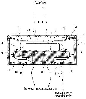
As shown in FIG. 1, the radiological image pickup apparatus
of the embodiment includes a radiation detection section having
an active matrix substrate 6, a radiation-sensitive
semiconductor 7, and a voltage application electrode 8. The
active matrix substrate 6 is formed with a charge-storage
capacitor, a charge read thin-film transistor (TFT) switching
element, and a pixel electrode for each unit cell with signal
lines and scanning lines disposed like a lattice on the
insulating substrate such as a glass substrate. The
radiation-sensitive semiconductor 7 is made of amorphous
selenium for producing charges as radiation is incident and
is formed on the active matrix substrate 6. The voltage
application electrode 8 is provided on the surface of the
radiation-sensitive semiconductor 7 on which radiation is
incident. The radiation-sensitive semiconductor 7 made of
amorphous selenium is a high-purity amorphous selenium (a-Se)
11
CA 02462407 2004-03-30
,,..-
thick filmwith specific resistance of 10952cmormore (preferably
10'lf2cm or more) and having a film thickness ranging from about
0.5 mm to about 1.5 mm. This a-Se thick film has excellent
suitability particularly for putting the detection area into
a large area.
The active matrix substrate 6 is connected to a signal
processing circuit 10 by a flexible wiring film 11 and is driven
by an LSI chip disposed on the film 11, and a signal detected
by the radiation-sensitive semiconductor 7 and output through
the active matrix substrate 6 is subjected to processing of
amplification, etc., by the LSI chip 9.
FIG. 2 is a drawing to show the active matrix substrate
6, the configuration of the LSI chip 9, and an outline of the
signal processing circuit 10. The active matrix substrate 6
has pixel electrodes 6a and charge-storage capacitors 6b
provided in a one-to-one correspondence with the pixel
electrodes 6a for temporarily retaining detected signal charges
(in FIG. 2, each charge-storage capacitor 6b is positioned below
the corresponding pixel electrode 6a) . Switching elements 6c
are driven on and off for each row by a drive signal supplied
through scanning lines 6e and the stored signal charges are
output through the switching elements 6c and signal lines 6d
and are amplified by charge detection amplifiers 91 and then
are output to the signal processing circuit 10. A multiplexer
l0a of the signal processing circuit 10 selects the signal for
12
CA 02462407 2004-03-30
each column in sequence and outputs the signal to anA/D converter
10b, and the signal is subjected to predetermined signal
processing in an image processing circuitto provide a photograph
image. The charge detection amplifiers 91 and a gate driver
92 are integrated on the LSI chip 9 shown in FIG. 1.
FIG. 3 is a drawing to describe the circuit configuration
of the portion corresponding to one pixel unit DU of the active
matrix substrate 6, etc. Fig. 3 schematically shows only the
portion corresponding to the pixel electrode 6a in the
radiation-sensitive semiconductor 7 and the voltage
application electrode 8. In FIG. 3, a bias voltage is applied
to the voltage application electrode 8 from a bias supply power
supply 20 and in the pixel on which radiation is incident, charges
produced in response to the interaction with the
radiation-sensitive semiconductor 7 are transferred by a bias
electric field, whereby the charges are induced to the pixel
electrode 6a and are stored in the charge-storage capacitor
6b corresponding to the pixel. The switching element 6c is
driven on and off by the gate driver 92. When it is turned
on, the stored signal charges are sent through a drain 6f and
the signal line 6d to the charge detection amplifier 91, which
then amplifies the signal charges and outputs the amplified
signal charges to the signal processing circuit 10.
In FIG. 1, the radiation-sensitive semiconductor 7 and
the voltage application electrode 8 on the active matrix
13
CA 02462407 2004-03-30
substrate 6 are molded so as to cover the whole of the
radiation-sensitive semiconductor 7 and the voltage
application electrode 8 in such a manner that an insulating
substance 41 such as an epoxy adhesive is poured into the area
surrounded by an insulating weir member 43 made of resin and
an insulating plate member 42 such as a glass plate is bonded
and formed. Thus, a shield member 3 formed of a conductive
material can be brought close to the proximity of the pole of
the voltage application electrode 8, and it is made possible
to provide the shield effect more perfectly.
Thus, the active matrix substrate 6 is formed in a state
in which it is shielded with the radiation-sensitive
semiconductor 7 and the voltage application electrode 8. The
active matrix substrate 6 is fixed on a bed 30 and is disposed
in a cabinet 1. The cabinet 1 is made up of a surface lid section
la and a non-surface lid section lb. The surface lid section
la is formed of a nonconductive material of plastic, etc. , and
the non-surface lid section lb is formed of a conductive material.
A cooling fan 12 is disposed at the bottom of the non-surface
lidsection lb for releasing air in the cabinet 1 into the outside
to provide a cooling function.
The structure is adopted, whereby a capacitor is not formed
between the voltage application electrode and the surface lid
section of the cabinet andwhen a bias voltage is applied, charges
are not stored. Thus, if the cooling fan, etc., causes the
14
CA 02462407 2004-03-30
,....
surface lid section to vibrate, charge transfer does not occur
and noise is not detected. Consequently, it is made possible
to thin as much as possible the surface lid section of the cabinet
also serving as an incidence window member of radiation.
on the insulating plate member 42, the shield member 3
made of a conductive material is disposed and shields in the
area from the outer frame of the cabinet 1 to the margin of
the voltage application electrode 8 so as to cover the area
other than the portion just above the voltage application
electrode 8. FIG. 4 is a three-dimensional drawing to represent
the shield relationship; the hatched portion is the shield
portion of the shield member 3 and the black portion of the
voltage application electrode 8 is an opening. FIG. 4 is a
schematic drawing and the portion of the non-surf ace lid section
lb is transparent; in fact, however, it need not be transparent
and the surface lid section la of the cabinet 1 (FIG. 1) is
removed in FIG. 4.
The structure is adopted, whereby electrostatic noise
occurring as the surface lid section la vibrates with vibration
of the cooling fan 12, etc., with the surface lid section la
naturally charged does not enter the charge detection amplifiers
91 or the gate driver 92 and does not have a detrimental effect
thereon. Therefore, it is made possible to thin as much as
possible the surface lid section la of the cabinet 1 also serving
as an incidence window member of radiation.
CA 02462407 2004-03-30
,..,,
The radiation-sensitive semiconductor 7 and the voltage
application electrode 8 on the active matrix substrate 6 are
molded by using the insulating substance 41, the insulating
plate member 42, and the insulating weir member 43 so as to
cover the whole of the radiation-sensitive semiconductor 7 and
the voltage application electrode B. Therefore, the shield
member 3 can be brought close to the proximity of the pole of
the voltage application electrode 8 and the shield effect is
provided more perfectly.
Preferably, the surface lid section la of the cabinet
1 is formed of a nonconductive material on the full face as
in the embodiment; however, the effect is provided if at least
the portion of the surface lid section la of the cabinet 1 opposed
to the voltage application electrode 8 is nonconductive. The
surface lid section la may be formed using a plate member of
a nonconductive material corresponding to the portion opposed
to the voltage application electrode 8 and a plate member formed
of a conductive material forming any other portion in combination.
The surface lid section la may be shaped like a curved surface
rather than a flat plate. Various commercially available
materials other thanplastic can also be applied; it is desirable
that a material having a high light blocking effect should be
used or light shield treatment should be conducted so as to
block visible light. Further, it is desirable that the
non-surface lid section lb should be formed of a conductive
16
CA 02462407 2004-03-30
.+.,.
material, but all need not necessarily be formed of a conductive
material.
Resin material (plastic) of ABS, phenol, vinyl chloride,
melamine, fluorine, acryl, polycarbonate, etc., or anon-resin
material of glass, ceramics, etc., can be used as the
nonconductive material used for the surface lid section la of
the cabinet 1. An alloy consisting essentially of Al, Fe, Ti,
Cu, Co, Ni, etc., or a molded article consisting essentially
of carbon can be used as the conductive material used for the
cabinet 1 and the surface lid section la.
In the example in FIG. 1, the insulating substance 41
such as an epoxy adhesive is poured into the area surrounded
by the insulating weir member 43 made of resin and the insulating
plate member 42 such as a glass plate is bonded and formed,
but the invention is not limited to the example. The invention
is also applied to a structure wherein the insulating plate
member 42 such as a glass plate does not exist, for example.
A plate member or a tape member consisting essentially
of aluminum, copper, etc., is also possible as the material
of the shield member, but the material is not limited to it.
If the shield area is made to overlap the inside of the margin
of the voltage application electrode 8 about as much as the
thickness of the insulating substance 41 for mold, the shield
effect can be provided more reliably. Further, if the rigidity
of the insulating substance 41 is high like epoxy in the
17
CA 02462407 2004-03-30
.+..,
embodiment and a sufficient thickness that can resist a
dielectric breakdown can be provided or the insulating plate
member 42 is covered with a hard material such as glass, the
shield area of the shield member 3 may be a shape covering the
whole portion rather than opening just above the voltage
application electrode 8.
Next, first to third modifications of the radiological
image pickup apparatus according to the embodiment will be
discussed. Parts identical with those previously described
with reference to FIG. 1 are denoted by the same reference
numerals in FIGS. 5 to 7. Tobeginwith, in the firstmodification
in FIG. 5, the LSI chip 9 on which the charge detection amplifiers
91 and the gate driver 92 are integrated shown in FIG. 2 is
formed on active matrix substrate 6 and the structure is molded
by using insulating substance 41, insulating plate member 42,
and insulating weir member 43 so as to cover the whole of the
LSI chip 9 together with radiation-sensitive semiconductor 7
and voltage application electrode 8. The structure is adopted,
whereby the whole can be made a flat shape and shield of shield
member 3 can be conducted easily and reliably. In FIG. 5, the
LSI chip 9 having the charge detection amplifiers 91 and the
gate driver 92 shown in FIG. 2 is installed on the active matrix
substrate 6 using a wire and a bump (not shown), but may be
formed integrally on the active matrix substrate 6 using a method
of photolithography, etc., like thin-film transistor (TFT)
18
CA 02462407 2004-03-30
~+.
switching elements.
In the second modification in FIG. 6, an accessory plate
31 made of a material of metal with high atom number 40 or more,
for example, Mo (42), Ag (47), In (49), Sn (50), W (74), or
Pb (82) is disposed on shield member 3 made of a conductive
material, for example, a copper plate for shielding the area
from the outer frame of cabinet 1 to the margin of voltage
application electrode 8 by screwing or with an adhesive or a
solvent. The material acts as a shield material of radiation
and can protect the parts of charge detection amplifiers 91
and gate driver 92 integrated on LSI chip 9 easily affected
by radiation damage.
In FIG. 6, the accessory plate 31 made of metal with high
atomnumber is disposedon the shieldmember 3, butmaybe attached
to the lower part of the shield member 3. The shield member
3 itself may be made of the accessory plate 31 made of metal
with a high atom number. The material made of metal with the
high atom number mentioned here may be, for example, a material
whose part is metal with high atom number as an Al plate and
a Pb plate are used in combination to provide strength.
Further, in the thirdmodification in FIG. 7, shieldmember
3 for shielding the area from cabinet 1 to the margin of voltage
application electrode 8 is provided with an extension 3a for
electrically connecting to the extension of non-surface lid
section lb of cabinet 1 made of a conductive material. The
19
CA 02462407 2004-03-30
connection method is not limited and may be a conductor,
conductive paste, crimp, screwing, etc. The extension of the
non-surface lid section lb of the cabinet 1 and the shieldmember
3 are thus connected, whereby it is made possible to more enhance
the shield effect on LSI chip 9, etc.
In the radiological image pickup apparatus of the
embodiment and the first to thirdmodifications described above,
the high-purity amorphous selenium (a-Se) thick film having
a film thickness ranging from about 0.5 mm to about 1.5 mm is
taken as an example of the radiation-sensitive semiconductor
7. However, the thickness can also be changed and an amorphous
semiconductor of selenium doped with alkali metal of Na, etc.,
halogen of Cl, etc., As, or Te or a selenium compound can also
be used depending on the type and application of radiation.
Any semiconductor of CdTe, CdZnTe, Pb12, Hg12, GaAs, Si, etc.,
other than selenium may be used.
However, the advantages of the invention remarkably
appear particularly when a high bias voltage is applied for
use like an amorphous semiconductor of amorphous selenium or
a selenium compound, because the higher the bias voltage, the
more easily charges are stored in the capacitor formed between
the voltage application electrode 8 and the portion
corresponding to the surface lid section la of the cabinet 1.
A charge blocking layer or a buffer layer may be provided
on both or either of the upper and lower layers of the
CA 02462407 2004-03-30
r.+.
radiation-sensitive semiconductor 7; they are collectively
defined as the radiation-sensitive semiconductor 7 in the
radiation detection section according to the embodiment. As
examples of the charge blocking layer and the buffer layer,
an amorphous semiconductor layer of selenium or a selenium
compound containing As or Te, an amorphous semiconductor layer
of selenium or a selenium compound doped with a minute amount
of halogen, alkalimetal,etc.,a high-resistance semiconductor
layer of Sb2S3, Ce02, CdS, etc., or the like can be named.
The voltage application electrode 8 is formed of proper
metal selected from among Au, Pt, Al, Ni, In, and the like or
ITO, etc. Of course, the materials of the radiation-sensitive
semiconductor 7, the charge blocking layer, the buffer layer,
and the voltage application electrode 8 are not limited to those
mentioned above.
Preferably, the non-surface lid section lb of the cabinet
1 is electrically connected to ground potential. In FIG. 1,
the active matrix substrate 6 and the cabinet are fixed directly
with an adhesive, a pressure sensitive adhesive, a fixture,
or the like, but the invention is also applied to the case where
they are fixed indirectly using any other jig of an Al plate,
etc.
According to the radiological image pickup apparatus
according to the first or second aspect of the present invention,
the portion corresponding to the surface lid section of the
21
CA 02462407 2004-03-30
cabinet is formed using a nonconductive material, so that a
capacitor is not formed between the voltage application
electrode and the surface lid section of the cabinet and when
a bias voltage is applied, charges are not stored. Thus, if
the surface lid section of the cabinet vibrates, noise does
not occur. Consequently, it is made possible to thin as much
as possible the surface lid section of the cabinet as an incidence
windowmemberof radiation. Thus, the S/N ratio canbe improved
largely.
According to the radiological image pickup apparatus
according to the third aspect of the present invention, further
any other portion than the portion in the cabinet opposed to
the voltage application electrode is formed of a conductive
material, so that the noise problem caused by vibration of the
surface lid section can be solved as in the invention as claimed
in claim 1 or 2, and it is made possible to sufficiently shield
the inside from an external magnetic field, etc., and it is
made possible to detect radiation with less noise.
According to the radiological image pickup apparatus
according to the fourth aspect of the present invention, the
area from the outer frame of the cabinet to the margin of the
voltage application electrode is shielded by a conductive
material so as to cover any other area than the portion just
above the voltage application electrode, so that electrostatic
noise occurring as the surface lid section of the cabinet formed
22
CA 02462407 2004-03-30
..~.
using a nonconductive material of plastic, etc., vibrates with
the surface lid section naturally charged is prevented from
entering the charge detection amplifiers or the gate driver.
The radiation-sensitive semiconductor and the voltage
application electrode on the active matrix substrate are molded
by using the insulating substance so as to cover the whole,
so that the conductive material can be brought close to the
proximity of the pole of the voltage application electrode and
it is made possible to provide the shield effect more perfectly.
According to the radiological image pickup apparatus of
the fifth aspect of the preset invention, the charge detection
amplifiers and the gate driver are formed on the active matrix
substrate and the structure is molded by using the insulating
substance so as to cover the whole together with the
radiation-sensitive semiconductor and the voltage application
electrode, so that the whole can be made a flat shape and shield
with the conductive material canbe conducted easily and reliably
to the proximity of the pole of the voltage application
electrode.
According to the radiological image pickup apparatus of
the sixth aspect of the present invention, the conductive
material for shielding the area from the outer frame of the
cabinet to the margin of the voltage application electrode is
a material made of metal with a high atom number such as tungsten
(W) or lead (Pb) or a material whose part is the metal with
23
CA 02462407 2004-03-30
,...._
a high atom number, so that the material acts as a shield material
of radiation and can protect the parts of the charge detection
amplifiers and the gate driver easily affected by radiation
damage, and the product life can be improved.
According to the radiological image pickup apparatus of
the seventh aspect of the present invention, the conductive
material for shielding the area from the outer frame of the
cabinet to the margin of the voltage application electrode is
electrically connected to the conductive portion of the cabinet,
so that the shield effect can be provided more reliably.
Particularly, to use the invention for amedical diagnosis
apparatus, the S/N ratio is improved and thus the application
amount of radiation can be reduced and exposure of patients
and diagnosis technicians to radiation can be decreased.
24