Note: Descriptions are shown in the official language in which they were submitted.
CA 02462762 2004-03-31
LIGHT EMISSION DIODE (LED)
BACKGROUND OF THE INVENTION
(a) Field of the Invention
s The present invention is related to a light emitting diode (LCD).
(b) Description of the Prior Art:
LED packaging technology of the prior art involves gluing light emission chips
to a frame, connection of metallic conductor between chips and frame, packaged
with
epoxy, and finally having the LEC welded to a PCB using the plug-in package
method.
io Whereas power dissipation of the LED of the prior art takes place at the
frame, power
dissipation in the form of heat is poor to cause higher junction temperature
of the light-
emitting chip and negatively affect the light emitting e~cacy and service
light of the
LED. Furthermore, the number of the distribution of the light emitting chips
by unit
area is comparatively lesser to be applicable in the ordinary illumination
that requires
is higher luminance. Therefore, the LED manufacturing industry has been
desperately
solving the problem of how to increase LED efficacy and service life by
lowering the
junction temperature of the light emitting chips, and the number of the number
of light
emitting chips of unit area so to fully utilize the advantages of longer
service life and
less power consumption of LED in the wider range of applications, and to make
LED
2 o the environment friendly product to replace the conventional lighting
source.
-1-
CA 02462762 2004-03-31
SUMMARY OF THE INVENTION
The primary purpose of the present invention is to provide a light emitting
diode
(LED) to significantly improve the power dissipation of the LED, lower the
junction
temperature of the light emitting chip, increase the light emitting efficacy
and service
s lift of the LED, and permit the number of the light emitting chip of unit
area, thus to
upgrade the light emitting efficiency of unit area.
To achieve the purpose, the LED is essentially comprised of heat conduction
substrate, circuitry provided on the heat conduction substrate, an insulation
layer
disposed between the heat conduction substrate and the circuitry, multiple
light
io emitting chips distributed among the circuitry and the space above the heat
conduction
substrate and connected to the circuitry through metal conductor, and a
protection layer
at the top of those light emitting chips.
Another purpose of the present invention is to provide a light emitting diode,
wherein, a recess or a trough is formed on the heat conduction substrate and
those Iight
is emitting chips are distributed at the bottom of the recess or trough while
being covered
up with a light permeable protection Layer.
Another purpose yet of the present invention is to provide a light emitting
diode,
wherein, a light permeable optical lens is provided on the light emitting chip
and fixed
to where above the light-emitting chip.
z o Another purpose yet of the present invention is to provide a light
emitting diode,
wherein, a circuit is formed among multiple light emitting chips through a
metal
conductor and both ends of the circuit is then connected to the circuitry on
the
substrate.
Another purpose yet of the present invention is to provide a light emitting
diode,
a s wherein, the LED is made into a module and multiple modules are
distributed on a
support board while a circuit or a conductor is used for connection among the
modules,
and the modules are locked to the support board.
Another purpose yet of the present invention is to provide a light emitting
diode,
wherein; the heat conduction substrate is made into a bow shape with light
emitting
3 o chips and circuitry distributed thereon.
-2-
CA 02462762 2004-03-31
Another purpose yet of the present invention is to provide a light emitting
diode,
wherein; a fan is adapted to the heat conduction substrate.
Those light emitting chips are distributed among the circuitry and in the
space
above the insulation layer, or glued among the circuitry and in the space
above the heat
s conduction substrate or the insulation layer.
Whereas the heat conduction substrate is provided, those light emitting chips
are
capable of fast dissipating the heat through the heat conduction substrate to
lower their
junction temperature, thus to increase effcacy and service life of the light
emitting
chip, and to realize the lay up of more light emitting chips on the unit area.
The
i o recess or the trough provided on the heat conduction substrate help
converge the light
and various circuitries can be arranged among the light emitting chips and/or
between
light emitting chips and the circuitry depending on the individual
application.
Furthermore, the light emitting chip can be made into various types of modules
for
mass production by lot and mounted on the support board depending on the
individual
is application to form a lighting source or light emitting source.
-3-
CA 02462762 2004-03-31
BRIEF DESCRIPTION OF THE DRAWINGS
Fig. 1 is a bird's view of a first preferred embodiment of the present
invention.
Fig. 2 is a blowup sectional view showing a local part of the first preferred
embodiment of the present invention.
s Fig. 3 is a blowup sectional view showing a local part of a second preferred
embodiment of the present invention.
Fig. 4 is a perspective view of a third preferred embodiment of the present
invention.
Fig. S is a bird's view of a fourth preferred embodiment of the present
invention.
to Fig. 6 is a bird's view of a fifth preferred embodiment of the present
invention.
Fig. 7 is a bird's view of a sixth preferred embodiment of the present
invention.
Fig. 8 is a sectional view taken from section A-A of the sixth preferred
embodiment of the present invention.
Fig. 9 is a bird's view of a seventh preferred embodiment of the present
i s invention.
Fig. 10 is a blowup sectional view showing a local part of the seventh
preferred
embodiment of the present invention.
Fig. 11 is a side view of an eighth preferred embodiment of the present
invention.
2 o Fig. 12 is a sectional view of a ninth preferred embodiment of the present
invention.
-4-
CA 02462762 2004-03-31
DETAILED DESCRIPTION OF THE PREFERRED EMBODIMENTS
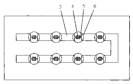
Referring to Figs. 1 and 2, a LED of the present invention includes a heat
conduction substrate 1; a circuitry 3 is provided on the heat conduction
substrate 1; an
insulation layer 2 is provided between the heat conduction substrate 1 and the
circuitry
3; multiple light emitting chips 4 are arranged among the circuit in the space
over the
heat conduction substrate; those light emitting chips 4 are each connected to
the
circuitry 3 by means of a metal conductor S; and those light emitting chips 4
are
covered up with a light permeable protection layer 6.
The heat conduction substrate 1 is made of ceramic material provided with good
i o aluminum and copper heat conduction property or any other material with
good heat
conduction property. The insulation layer 2 yields powerful insulation
property, and
the circuitry 3 on the top of the insulation layer 2 may be related to a
copper foil to be
etched with various circuits as required.
Those light emitting chips 4 are arranged among the circuit and in the space
over
i5 the heat conduction substrate 1, or among the copper foil and on the
insulation layer 2
above the heat conduction substrate 1. Furthermore, those light emitting chips
4 are
glued among the circuitry 3 and in the space over the heat conduction
substrate 1 or the
insulation layer 2. The light emitting chip 4 is each connected to the
circuitry 3 with
a metal conductor S and is covered up with the light permeable protection
layer 6.
a o The protection layer 6 is made of epoxy or silicon rubber in an arc form
for light
convergence and light color conversion. For example, when fluorescent powder
is
added into the protection layers, the blue light emitted from the light
emitting chip 4 is
converted into while light.
Whereas harder heat conduction materials with stronger heat conduction
25 property, the light emitting chip 4 for being firmly glued to the heat
conduction
substrate 1 rapidly dissipate the heat to significantly decrease the junction
temperature,
thus to increase its light emitting efficiency and service lift while
realizing the purpose
of having more light emitting chips 4 in smaller unit area. Furthermore, the
heat
conduction substrate 1 functions as a support for the LED.
3 o As illustrated in Fig. 3, an arc recess 7 is formed on the heat conduction
substrate 1 and those light emitting chips 4 are distributed at the bottom of
the arc
-5-
CA 02462762 2004-03-31
recess 7, and connected to the circuitry 3 with a metal conductor 5 a light
permeable
protection layer 6 covers up the light emitting chip 4 and the arc recess 7.
The arc
recess 7 reflects the light emitted from the light emitting chip 4 and refract
the light
towards a direction away from the substrate 1 to increase light emitting
efficiency and
s enlarge the contact area with the heat conduction substrate 1 for further
enhancing heat
conduction result between the light emitting chip 4 and the heat conduction
substrate
1.
A third preferred embodiment of the present invention as illustrated in Fig. 4
is
provided with a light permeable optical lens 11 with four footages 12 on the
light
io emitting chip 4. Four respective holes 13 are respectively provided on the
peripheral
of the light emitting chip 4 on the heat conduction substrate 1 to fix the
optical lens 11
above the light emitting chip 4. Accordingly, the light from the light
emitting chip 4
is transmitted through the optical lens 11. Alternatively, the optical lens 11
is
forthwith adhered to the heat conduction substrate 1.
is A fourth preferred embodiment of the present invention as illustrated in
Fig. 5,
three light emitting chips 4 are at the same time distributed on the bottom of
the recess
7 and are respectively connected to the circuitry 3 with the metal conductor
5. As
illustrated in Fig. 6, three light emitting chips 4 are connected in series
through the
metal conductor 5 in a fifth preferred embodiment of the present invention,
and then
z o both ends of the series circuit is connected to the circuitry 3. Figs. 7
and 8 show a
sixth preferred embodiment of the present invention, wherein, a trough 8 is
formed on
the heat conduction substrate among the circuitry 3 with each of those light
emitting
chip 4 connected to the circuitry 3 through the metal conductor 5.
Alternatively, a
series circuit is formed first with metal conductor among those light emitting
chips 4
z s and having both ends of the series circuit to be connected to the
circuitry 3.
Depending on the individual application, various circuit structures are formed
between
those light emitting chips 4 and the circuitry 3 for those light emitting
chips 4 to be
directly connected to the circuitry 3, or a parallel or a series circuit is
formed first
among those light emitting chips 4 before being connected to the circuitry 3
on the
3 o heat conduction substrate 1.
As described above, the light emitting chip 4 is capable of rapidly
dissipating the
-6-
CA 02462762 2004-03-31
heat. Given with the premises that each light emitting chip 4 is provided with
the
same light emitting efficiency and service lift, number of the Light emitting
chip 4 on
the unit area can be increased to improve the light emitting strength of the
unit area.
Figs. 9 and 10 illustrated a seventh preferred embodiment of the present
s invention. Wherein, multiple LEDs of the present invention are made into
modules 9
and distributed on a support board 10 while circuitry or metal conductor is
used to
connect among those modules, and those modules 9 are riveted or glued to the
support
board 10. Accordingly, the LED module can be realized with mass production by
lot to be distributed on the support board in various forms and areas
depending on the
i o individual application. The support board I O is made of a material of
good heat
conduction property to help fast dissipate the heat from the heat conduction
substrate
1.
In an eighth preferred embodiment of the present invention as illustrated in
Fig.
11, the heat conduction substrate 1 is made into a bow shape with those light
emitting
i s chips 4 and the circuitry distributed thereon; or alternatively, the heat
conduction
substrate 1 can be made into various surfaces depending on the individual
application.
The heat conduction substrate 1 is intergraded with a power dissipation member
I4 as illustrated in Fig. 12 for a ninth preferred embodiment of the present
invention.
Wherein, the power dissipation member 14 can be made into a stick, a sheet or
in any
a o other form that facilitates power dissipation.
Furthermore, a fan is provided on the heat conduction substrate 1 to lower its
temperature and thus reduces the size of the heat conduction substrate I while
improving the light emitting efficiency and service life of the light emitting
chip 4.