Note: Descriptions are shown in the official language in which they were submitted.
CA 02463486 2004-04-08
WO 2004/019314 PCT/JP2003/010644
1
D E S C R I P T I 0 N
DISPLAY DEVICE AND DISPLAY DEVICE DRIVING METHOD
Technical Field
The present invention relates to a display device
and a display device driving method.
Background Art
Liquid crystal displays are, generally classified
into active matrix driving liquid crystal displays and
simple matrix driving liquid crystal displays. The
active matrix driving liquid crystal display displays
an image having a higher luminance, higher contrast,
and higher resolution as compared to the simple matrix
driving liquid crystal display. In the active matrix
driving liquid crystal display, a liquid crystal
element which also functions as a capacitor and a
transistor which activates the liquid crystal element
are arranged for each pixel. In the active matrix
driving liquid crystal display, a selection signal is
input from a scanning driver serving as a shift
register to a scanning line so that the scanning line
is selected. At this time, when a voltage having a
level representing a luminance is applied from a data
driver to a signal line; the voltage is applied to the
liquid crystal element through the transistor. Even
when the transistor is turned off during a period from
CA 02463486 2004-04-08
WO 2004/019314 PCT/JP2003/010644
2
the end of signal input to the scanning.line to the
next signal input, the voltage level is held until the
next signal is input to the scanning line because the
liquid crystal element functions as a capacitor. As
described above, while the signal is input to the
scanning line, the light transmittance of the liquid
crystal element is newly refreshed. Light from a
backlight passes through the liquid crystal element at
the refreshed light transmittance so that the gray
level of the liquid crystal display is expressed.
On the other hand, an organic EL
(ElectroLuminescence) display which uses organic EL
elements as spontaneous optical elements requires no
backlight, unlike liquid crystal displays. Hence, the
organic EL display is optimum for a thin display. In
addition, the organic EL display has no limitation on
the angle of field, unlike liquid crystal displays.
For this reason, practical utilization of organic EL
displays as next-generation display devices is greatly
expected.
From the viewpoint of a high luminance, high
contrast, and high resolution, voltage-controlled
active matrix driving schemes have been developed not
only for liquid crystal displays but also for organic
EL displays. However, the capacity of an organic EL
element is much smaller than that of a liquid crystal
element so a current flows to the organic EL element
CA 02463486 2004-04-08
WO 2004/019314 PCT/JP2003/010644
3
itself. To hold a voltage, the number of transistors
increases. This leads to an increase in complexity of
a circuit constituted by transistors.
In a transistor, generally, the channel resistance
changes due to a change in ambient temperature or
long-time use. For this reason, the gate threshold
voltage changes over time or varies between
transistors. It is therefore difficult to uniquely
designate the current level to be supplied to an
organic EL element on the basis of the gate voltage
level of a switching transistor by changing the value
of the voltage to be applied to the gate electrode of
the transistor and thus changing the level of the
current to be supplied to the organic EL element. In
other words, the level of the current to be supplied
can hardly be uniquely designated by changing the value
of the voltage to be applied to the gate electrode of
the transistor and thus changing the luminance of the
organic EL element. That is, even when a gate voltage
of the same level is applied to the transistors of a
plurality of pixels, the organic EL elements of the
plurality of pixels may have different emission
luminances. This may cause a variation in luminance on
the display screen.
Disclosure of Invention
It is an object of the present invention to
provide a display device and a display device driving
CA 02463486 2004-04-08
WO 2004/019314 PCT/JP2003/010644
4
method, which allow stable display on the basis of a
simple driving principle.
In order to solve the above problems, according to
an aspect of the present inzrention, there is provided a
display device comprising:
a plurality of scanning lines (e. g., selection
scanning lines X1 to Xm);
a plurality of signal lines (e.g., signal lines Y1
to Yn):
a scanning driver (e. g., a selection scanning
driver 5) which sequentially supplies to the scanning
lines selection signals that select the scanning lines;
a data driver (e. g., a data driver 3) which
supplies a designation current (e. g., a gray level
designation current IDATA) to the p3urality of signal
lines within a selection period (e. g., a selection
period TSE) when the scanning lines are being selected;
a plurality of pixel circuits (e. g., pixel
circuits D1~1 to Dm~n) which supplies a driving current
corresponding to a current value of the designation
current that flows to the signal lines;
a plurality of optical elements (e. g., light-
emitting elements E1~1 to Em~n) which emit light in
accordance with the driving current supplied by the
plurality of pixel circuits; and
a power supply (e. g., a common signal power supply
6) which outputs to the plurality of pixel circuits a
CA 02463486 2004-04-08
WO 2004/019314 PCT/JP2003/010644
driving current reference voltage (e. g., a voltage
VHIGH~ to supply the driving current.
In the above device, in accordance with the timing
when the power supply outputs the driving current
5 reference voltage, the plurality of pixel circuits
supply the driving current in accordance with the
current value of the designation current that flows
within each selection period. Accordingly, the optical
elements emit light.
Hence, when the power supply outputs the driving
current reference voltage from the end of the selection
period of a predetermined scanning line till the
beginning of the selection period of the next scanning
line, a driving current corresponding to both an
optical element corresponding to the predetermined
scanning line and an optical element corresponding to
the next scanning line flows. Hence, the optical
elements can emit light at a desired luminance.
When the power supply outputs the driving current
reference voltage to the pixel circuit at once after
all the scanning lines are selected, all the optical
elements can emit light.
When a reset voltage is output to the plurality of
signal lines within a period when none of the plurality
of optical elements are selected, the signal lines
reset charges stored in the preceding selection period.
For this reason, the parasitic capacitance of the
CA 02463486 2004-04-08
WO 2004/019314 PCT/JP2003/010644
6
signal lines can be quickly charged within the next
selection period so that even when a designation
current having a smaller current value is supplied, the
current value of the designation current can rapidly be
set in the steady state. Hence, even an optical
element such as an organic EL element whose luminance
is modulated by a small current on the ,uA order is
allowed to quickly display multiple gray level
luminances.
Brief Description of Drawings
FIG. 1 is a view showing an organic EL display
applied as a display device according to the first
embodiment of the present invention;
FIG. 2 is a plan view showing a pixel shown in
FIG. 1, in which an oxide insulating film, channel
protective insulating film, and common electrode are
omitted to help understanding;
FIG. 3 is a sectional view taken along a line
III - III in FIG. 2;
20-- FIG. 4 is a sectional view taken along a line
IV - IV in FIG. 2;
FIG. 5 is a sectional view taken along a line
V - V in FIG. 2;
FIG. 6 is an equivalent circuit diagram of four
adjacent pixels;
FIG. 7 is a graph showing the current vs. voltage
characteristic of an N-channel field effect transistor
CA 02463486 2004-04-08
WO 2004/019314 f PCT/JP2003/010644
7
used in the first embodiment;
FIG. 8 is a timing chart showing the levels of
signals in the apparatus according to the first
embodiment;
FIG. 9A is a view showing a voltage state when no
switching circuit is arranged, and a gray level
designation current with the maximum current value is
supplied across the drain and source of a transistor
and a signal line during the selection period of the
ith row;
FIG. 9B is a view showing a voltage state when a
switching circuit is arranged, and a gray level
designation current with the maximum current value is
supplied across the drain and source of a transistor
and a signal line during the selection period of the
ith row;
FIG. 10 is a view showing an organic EL display
applied as a display device according to the second
embodiment of the present invention, in which a common
signal power supply is arranged in a controller;
FIG. 11 is a view showing an organic EZ display
applied as a display device according to the third
embodiment of the present invention, in which the drain
of the transistor of a pixel circuit is connected to a
selection scanning line;
FIGS. 12A and 12B are equivalent circuit diagrams
showing adjacent pixels in the third embodiment to
CA 02463486 2004-04-08
WO 2004/019314 PCT/JP2003/010644
8
indicate current flows in different operation periods
and
FIG. 13 is a timing chart showing the levels of
signals in the apparatus according to the third
embodiment.
Best Mode for Carrying Out the Invention
Detailed embodiments of the present invention will
be described below with reference to the accompanying
drawings. The scope and spirit of the display device
or panel are not limited to the illustrated
embodiments.
[First Embodiment]
FIG. 1 is a view showing an organic EL display to
which the present invention is applied. An organic EL
display 1 comprises, as a basic arrangement, an organic
EL display panel 2, data driver 3, selection scanning
driver 5, common signal power supply 6, switching
circuit 7, and controller 11.
In the organic EL display panel 2, a display
section 4 on which an image is actually displayed is
formed on a transparent substrate 8. The data driver
3, selection scanning driver 5, common signal power
supply 6, and switching circuit 7 are arranged around
the display section 4. The data driver 3, selection
scanning driver 5, and common signal power supply 6 may
be arranged either on the transparent substrate 8 or
on a flexible circuit board arranged around the
CA 02463486 2004-04-08
WO 2004/019314 PCT/JP2003/010644
9
transparent substrate 8.
In the display section 4, (m ~ n) pixels P1~1 to
Pm,n (m and n are arbitrary natural numbers) are
arranged in a matrix on the transparent substrate 8.
In the column direction, i.e., in the vertical
direction, m pixels Pl~j to Pm~j (j is an arbitrary
natural number; 1 ~ j ~ n) are arrayed. In the row
direction, i.e., in the horizontal direction, n pixels
Pi,1 to Pi,n (i is an arbitrary natural number; 1
i ~ m) are arrayed. That is, a pixel which exists on
the ith line (i.e., the ith row) from the upper side in
the vertical direction and the jth line (i.e., the jth
column) from the left side in the horizontal direction
is defined as a pixel Pi~j.
In the display section 4, m selection scanning
lines X1 to Xm running in the row direction are
parallelly arranged in the column direction on the
transparent substrate 8. In addition, m common signal
supply lines Z1 to Zm running in the row direction are
parallelly arranged in the column direction on the
transparent substrate 8 in correspondence with the
selection scanning lines X1 to Xm. Each common signal
supply line Zk (1 ~ k ~ m-1) is inserted between the
selection scanning lines Xk and Xk+1. The selection
scanning line Xm is inserted between the common signal
supply lines Zm_1 and Zm. In addition, n signal lines
Y1 to Yn running in the column direction are parallelly
CA 02463486 2004-04-08
WO 2004/019314 PCT/JP2003/010644
arranged in the row direction on the transparent
substrate 8. The selection scanning lines X1 to Xm,
common signal supply lines Z1 to Zm, and signal lines
Y1 to Yn are insulated from each other by intervening
5 insulating films. A selection scanning line Xi and
common signal supply line Zi are connected to n pixels
Pi,1 to Pi,n arrayed in the row direction. A signal
line Y~ is connected to m pixels Pi~~ to Pm~~ arrayed
in the column direction. The pixel Pi~~ is arranged at
10 a portion surrounded by the selection scanning line Xi,
common signal supply line Zi, and signal line Y~. The
selection scanning lines X1 to Xm are connected to the
output terminals of the selection scanning driver 5.
The common signal supply lines Z1 to Zm are rendered
conductive to each other and connected to the output
terminal of the common signal power supply 6. That is,
the same signal is output to the common signal supply
lines Z1 to Zm.
The pixel Pi~~ will be described next with
reference to FIGS. 2 to 6. FIG. 2 is a plan view
showing the pixel Pi~~. To help understanding, an
oxide insulating film 41, channel protective insulating
film 45, and common electrode 53 (to be described
later) are omitted. FIG. 3 is a sectional view taken
along a line III - III in FIG. 2. FIG. 4 is a
sectional view taken along a line IV - IV in FIG. 2.
FIG. 5 is a sectional view taken along a line V - V in
CA 02463486 2004-04-08
WO 2004/019314 PCT/JP2003/010644
11
FIG. 2.
FIG. 6 is an equivalent circuit diagram of four
adjacent pixels Pi~j, Pi+l,j~ Pi,j+1~ and Pi+1,j+1~
The pixel Pi~j is constituted by a light-emitting
element Ei~j which emits light with a luminance (nt. -
cd/m2) corresponding to the current value of the
driving current and a pixel circuit Di~j which is
arranged around the light-emitting element Ei~j and
drives the light-emitting element Ei~j. The pixel
circuit Di~j holds the current value of a current that
flows to the light-emitting element Ei~j during a
predetermined light-emitting period on the basis of a
voltage signal and current output from the data driver
3, selection scanning driver 5, power supply scanning
driver 6, and switching circuit 7. With this
operation, the luminance of the light-emitting element
Ei~j is held at a predetermined value during a
predetermined period.
The light-emitting element Ei~j is made of an
organic EL element. The light-emitting element Ei~j
has a multilayered structure formed by sequentially
stacking a pixel electrode 51, an organic EL layer 52,
and the common electrode 53. The pixel electrode 51
functions as an anode on the transparent substrate 8.
The organic EL layer 52 has a function of receiving
holes and electrons by an electric field and a function
of transporting holes and electrons. The organic EL
CA 02463486 2004-04-08
WO 2004/019314 a PCT/JP2003/010644
12
layer 52 has a recombination region where the
transported holes and electrons are recombined'and a
light-emitting region where light is emitted by
capturing excitons generated upon recombination. The
organic EL layer 52 functions as a light-emitting layer
in a broad sense. The common electrode 53 functions as
a cathode.
The pixel electrode 51 is patterned and separated
for each pixel Pi~j in each surrounded region
surrounded by the signal lines Y1 to Yn and selection
scanning lines X1 to Xm. The peripheral edge of the
pixel electrode 51 is covered with an interlayer
dielectric film 54 which has a layer of silicon nitride
or silicon oxide that covers three transistors 21, 22,
and 23 of the pixel circuit Di~j. The upper surface at
the center of the pixel electrode 51 is exposed through
a contact hole 55 in the interlayer dielectric film 54.
The interlayer dielectric film 54 may also have a
second layer formed of an insulting film of polyimide
or the like on the first layer of silicon nitride or
silicon oxide.
The pixel electrode 51 has conductivity and
transmittance to visible light. The pixel electrode 51
preferably has a relatively high work function and
efficiently injects holes into the organic EL layer 52.
For example, the pixel electrode 51 contains, as a
principal component, indium tin oxide (ITO), indium
CA 02463486 2004-04-08
WO 2004/019314 PCT/JP2003/010644
13
zinc oxide, indium oxide (In203), tin oxide (Sn02), or
zinc oxide ( Zn0) .
The organic EL layer 52 is formed on each pixel
electrode 51. The organic EL layer 52 is also
patterned for each pixel Pi~j. The organic EL layer 52
contains a light-emitting material (phosphor) as an
organic compound. The light-emitting material may be
either a polymeric material or a low molecular weight
material. The organic EL layer 52 may have, e.g., a
two-layered structure in which a hole transport layer
52A and a light-emitting layer 52B in a narrow sense
are formed sequentially from the side of the pixel
electrode 51, as shown in FIG. 3. The light-emitting
layer 52B has a recombination region where holes and
electrons are recombined and a light-emitting region
where light is emitted by capturing excitons generated
upon recombination. Alternatively, the organic EL
layer 52 may have a three-layered structure in which a
hole transport layer, a light-emitting layer in a
narrow sense, and electron transport layer are formed
sequentially from the side of the pixel electrode 51.
The organic EL layer 52 may have a single-layered
structure including a light-emitting layer in a narrow
sense. The organic EL layer 52 may also have a
multilayered structure formed by interposing an
electron or hole injection layer between appropriate
layers of the above layer structure. The organic EL
CA 02463486 2004-04-08
WO 2004/019314 -~ PCT/JP2003/010644
14
layer 5~2 may have any other layer structure.
The organic EL display panel 2 is capable of
full-color display or mult?.-color display. In this
case, the organic EL layer 52 of each of the pixels
Pi,1 to Pi,n is formed of a light-emitting layer in a
broad sense, which has a function of emitting one of,
e.g., red light, green light, and blue light. That is,
when the pixels Pi~1 to Pin selectively emit red,
green, and blue light, a color tone is displayed by
appropriately synthesizing the colors.
The organic EL layer 52 is preferably made of an
organic compound that is electronically neutral. In
this case, holes and electrons are injected and
transported in the organic EL layer 52 in good balance.
In addition, an electron transportable substance may be
appropriately mixed into the light-emitting layer in a
narrow sense. A hole transportable substance may be
appropriately mixed into the light-emitting layer in a
narrow sense. An electron transportable substance and
a hole transportable substance may be appropriately
mixed into the light-emitting layer in a narrow sense.
A charge transport layer serving as an electron
transport layer or a hole transport layer may be caused
to function as a recombination region. Light may be
emitted by mixing phosphor into the charge transport
layer.
The common electrode 53 formed on the organic EL
CA 02463486 2004-04-08
WO 2004/019314 PCT/JP2003/010644
layer 52 is a single electrode connected to all the .
pixels P1~1 to Pm~n. Alternately, the common electrode
53 may comprise a plurality of stripe-shaped electrodes
connected to the respective columns. More specifi-
5 cally, the common electrode 53 may comprise a stripe
common electrode connected to a group of pixels Pl,h-1
to Pm~h-1 (h is an arbitrary natural number; 2 <-_ h
n) in the column direction, a stripe common electrode
connected to a group of pixels Pl~h to Pm~h. In this
10 manner, the common electrode 53 comprises a plurality
of stripe-shaped electrodes each connected to each
column. Alternatively, the common electrode 53 may
comprise a stripe common electrode connected to a group
of pixels Pg_1~1 to Pg_1,n (g is an arbitrary natural
15 number; 2 ~ g ~ m) in the row direction, a stripe
common electrode connected to a group of pixels Pg~1 to
Pg~n,.... In this manner, the common electrode 53
comprises a plurality of stripe-shaped electrodes
connected to each row.
In any case, the common electrode 53 is
electrically insulated from the selection scanning line
Xi, signal line Y~, and common signal supply line Zi.
The common electrode 53 is made of a material having a
low work function. For example, the common electrode
53 is made of a single element or an alloy containing
at least one of indium, magnesium, calcium, lithium,
barium, and rare-earth metals. The common electrode 53
CA 02463486 2004-04-08
WO 2004/019314 PCT/JP2003/010644
16
may have a multilayered structure formed by stacking a
plurality of layers made of the above materials. More
specifically, the multilayered structure may include a
high purity barium layer which. has a low work function
and is formed on the side of the interface that is in
contact with the organic EL layer 52, and an aluminum
layer that covers the barium layer. Alternatively, the
multilayered structure may have a lithium layer on the
lower side and an aluminum layer on the upper side.
When a transparent electrode is used as the pixel
electrode 51, and light emitted from the organic EL
layer 52 of the organic EL display panel 2 should exit
from the side of the transparent substrate 8 through
the pixel electrode 51, the common electrode 53
preferably shields the light emitted from the organic
EL layer 52. More preferably, the common electrode 53
has a high reflectance against the light emitted from
the organic EL layer 52.
As described above, in the light-emitting element
Ei~j having a multilayered structure, when a forward
bias voltage is applied between the pixel electrode 51
and the common electrode 53, holes are injected from
the pixel electrode 51 to the organic EL layer 52 while
electrons are injected from the common electrode 53 to
the organic EL layer 52. The holes and electrons are
transported in the organic EL layer 52. When the holes
and electrons are recombined in the organic EL layer
CA 02463486 2004-04-08
WO 2004/019314 PCT/JP2003/010644
17
52, excitons are generated. The excitons excite the
organic EL layer 52. The organic EL layer 52 emits
light.
The emission luminance (unit: nt. - cd/m2) of the
light-emitting element Ei~~ depends on the current
value of the current that flows to the light-emitting
element Ei~~. To maintain a predetermined emission
luminance of the light-emitting element Ei~~ during the
light-emitting of the light-emitting element Ei~~ or
obtain an emission luminance corresponding to the
current value of a gray level designation current IDATA
drawn from the data driver 3, the pixel circuit Di~~ is
arranged around the light-emitting element Eis~ of each
pixel Pi~~. The pixel circuit Di~~ controls the
current value of the light-emitting element Ei~~.
Each pixel circuit Di~~ comprises three
transistors 21, 22, and 23 and a capacitor 24. Each
transistor is formed of a field effect thin film
transistor (TFT) having an N-channel MOS structure.
Each transistor 21 is an MOS field effect
transistor constituted by a gate electrode 21g, gate
insulating film 42, semiconductor layer 43, source
electrode 21s, and drain electrode 21d. Each
transistor 22 is an MOS field effect transistor
constituted by a gate electrode 22g, gate insulating
film 42, semiconductor layer 43, source electrode 22s,
and drain electrode 22d. Each transistor 23 is
CA 02463486 2004-04-08
WO 2004/019314 PCT/JP2003/010644
18
constituted by a gate electrode 23g, gate insulating
film 42, semiconductor layer 43, source electrode 23s,
and drain electrode 23d.
More specifically, as shown in FIG. 3, the first
transistor 21 is a reverse stagger type transistor
comprising the gate electrode 21g, oxide insulating
film 41, gate insulating film 42, island-shaped
semiconductor layer 43, channel protective insulating
film 45, impurity-doped semiconductor layers 44, source
electrode 21s, and drain electrode 21d. The gate
electrode 21g is made of aluminum and formed on the
transparent substrate 8. The oxide insulating film 41
is formed by anodizing aluminum that covers the gate
electrode 21g. The gate insulating film 42 is made of
silicon nitride or silicon oxide and covers the oxide
insulating film 41. The semiconductor layer 43 is
formed on the gate insulating film 42. The channel
protective insulating film 45 is made of silicon
nitride and formed on the gate insulating film 42. The
impurity-doped semiconductor layers 44 are made of
n+-silicon and formed at both ends of the semiconductor
layer 43. The source electrode 21s and drain electrode
21d are made of a material selected from chromium, a
chromium alloy, aluminum and an aluminum alloy, and
formed on the impurity semiconductor layers 44.
The second and third transistors 22 and 23 have
the same structure as that of the first transistor 21
CA 02463486 2004-04-08
WO 2004/019314 PCT/JP2003/010644
19
described above. However, the shapes, sizes, and
dimensions of the transistors 21, 22, and 23, and the
channel widths and channel lengths of the semiconductor
layers 43 are appropriately set in accordance with the
functions of the transistors 21, 22, and 23.
The transistors 21, 22, and 23 may be formed
simultaneously by the same process. In this case, the
gate electrodes, oxide insulating films 41, gate
insulating films 42, semiconductor layers 43, impurity
semiconductor layers 44, source electrodes, and drain
electrodes of the transistors 21, 22, and 23 have the
same compositions.
Even when the semiconductor layers 43 of the
transistors 21, 22, and 23 are made of amorphous
silicon, they can be sufficiently driven. However, the
semiconductor layers 43 may be made of polysilicon.
The structures of the transistors 21, 22, and 23 are
not limited to the reverse stagger type. Even a
stagger type or coplanar type structure may be
employed.
Each capacitor 24 is constituted by an electrode
24A, electrode 24B, and dielectric body. The electrode
24A is connected to the gate electrode 23g of the third
transistor 23. The electrode 24B is connected to the
source electrode 23s of the transistor 23. The
dielectric body has the gate insulating film 42
interposed between the electrodes 24A and 24B. The
CA 02463486 2004-04-08
WO 2004/019314 PCT/JP2003/010644
capacitor 24 stores charges between the source
electrode 23s and the drain electrode 23d of the
transistor 23.
As shown in FIG. 6, in the second transistor 22 of
5 each of the pixel circuit Di~1 to Din of the ith row,
the gate electrode 22g is connected to the selection
scanning line Xi of the ith row. The drain electrode
22d is connected to the common signal supply line Zi of
the ith row. As shown in FIG. 5, the drain electrode
10 23d of the third transistor 23 of each of the pixel
circuit Di~1 to Din of the ith row is connected to the
common signal supply line Zi of the ith row through a
contact hole 26. The gate electrode 21g of the first
transistor 21 of each of the pixel circuit Di~1 to Di,n
15 of the ith row is connected to the selection scanning
line Xi of the ith row. The source electrode 21s of
the transistor 21 of each of the pixel circuit Dl~j to
Dm~j of the jth column is connected to the signal line
Yj of the jth column.
20 In each of the pixels P1~1 to Pmsn, the source
electrode 22s of the second transistor 22 is connected
to the gate electrode 23g of the third transistor 23
through a contact hole 25 formed in the gate insulating
film 42, as shown in FIG. 4. The source electrode 22s
is also connected to one electrode of the capacitor 24.
The source electrode 23s of the transistor 23 is
connected to the other electrode of the capacitor 24
CA 02463486 2004-04-08
WO 2004/019314 ' PCT/JP2003/010644
21
and also to the drain electrode 21d of the transistor
21. The source electrode 23s of the transistor 23, the
other electrode of the capacitor 24, and the drain
electrode 21d of the transistor 21 are connected to the
pixel electrode 51 of the light-emitting element Ei~~.
The voltage of the common electrode 53 of the
light-emitting element Ei~~ is a reference voltage VSS.
In this embodiment, the common electrode 53 of all
light-emitting elements E1~1 to Em~n is grounded so
that the reference voltage VSS is set to 0 [V].
Protective films 43A formed by patterning the same
film as that of the semiconductor layers 43 of the
transistors 21 to 23 are arranged between the selection
scanning line Xi and the signal line Y~ and between the
common signal supply line Zi and the signal line Y~ as
well as the gate insulating film 42.
The controller 11 outputs a control signal group
pCNT including a data driver clock signal CK1, start
signal ST1 and latch signal L to the data driver 3 on
the basis of a dot clock signal CKDT, horizontal sync
signal HSyNC and vertical sync signal VSyNC, which are
input from the outside. The controller 11 also outputs
a control signal group GCNT including a selection
scanning driver clock signal CK2 and start signal ST2.
The controller 11 also outputs a common signal clock
signal CK3 to the common signal power supply 6. The
controller 11 also supplies a reset voltage VRST to the
CA 02463486 2004-04-08
WO 2004/019314 ' PCT/JP2003/010644
22
switching circuit 7 and outputs a switching signal
to the switching circuit 7.
More specifically, the data driver clock signal
CK1 is a signal to sequentially shift the selected
column in synchronism with the dot clock signal CKDT.
An 8-bit red digital gray level image signal SR, green
digital gray level image signal SG, and blue digital
gray level image signal Sg are received from an
external circuit at the timing of the clock signal CK1.
The start signal ST1 is a signal to return the selected
column to the first column in synchronism with the
horizontal sync signal HSyNC~ The latch signal L is a
signal to parallelly supply the analog gray level
designation current IDATA based on an analog gray level
designation signal to the signal lines Y1 to Yn. The
analog gray level designation signal is obtained by
causing the D/A converter in the data driver 3 to
D/A-convert the data of one row, i.e., the red digital
gray level image signal SR, green digital gray level
image signal SG, and blue digital gray level image
signal SB which. are received in correspondence with the
pixels Pi~1 to Pin.
The selection scanning driver clock signal CK2 is
a signal to sequentially shift the selected row in
synchronism with the horizontal sync signal HSyNC. The
start signal ST2 is a signal to return the selected row
to the first row in synchronism with the vertical sync
CA 02463486 2004-04-08
WO 2004/019314 PCT/JP2003/010644
23
signal VSyNC~
The common signal clock signal CK3 is a clock
signal to output a common signal to the common signal
supply lines Z1 to Zm.
The data driver 3, selection scanning driver 5,
and common signal power supply 6 arranged around the
display section 4 will be described next.
The selection scanning driver 5 is a so-called ,
shift register in which m flip-flop circuits are
connected in series. The driver 5 outputs a selection
signal to the selection scanning lines X1 to Xm. That
is, in accordance with the selection scanning driver
clock signal CK2 received from the controller 11, the
selection scanning driver 5 sequentially outputs a
, selection signal of ON level (high level) to the
selection scanning lines X1 to Xm in this order (the
selection scanning line X1 follows the selection
scanning line Xm), thereby sequentially selecting the
selection scanning lines X1 to Xm.
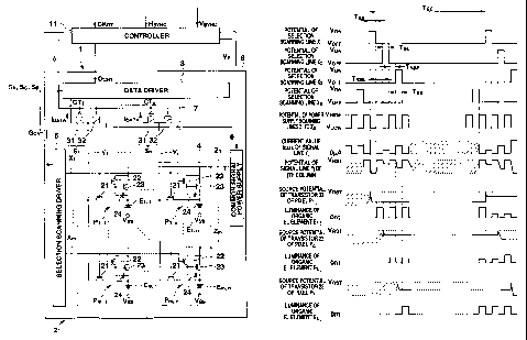
More specifically, as shown in FIG. 8, the
selection scanning driver 5 individually applies, to
the selection scanning lines X1 to Xm, one of an ON
voltage VON (e. g., much higher than the reference
voltage Vss) as a high-level selection signal and an
OFF voltage VOFF (e.g., equal to or lower than the
reference voltage Vs3) as a low-level selection signal,
thereby selecting each selection scanning line Xi at a
CA 02463486 2004-04-08
WO 2004/019314 PCT/JP2003/010644
24
predetermined period.
During a selection period TSE when the selection
scanning line Xi is to be selected, the selection
scanning driver 5 applies the ON voltage VON as a
selection signal of ON level (high level) to the
selection scanning line Xi. Accordingly, the
transistors 21 and 22 (the transistors 21 and 22 of all
the pixel circuits Di~1 to Din) connected to the
selection scanning line Xi are turned on. When the
first transistor 21 is turned on, the current that
flows to the signal line Y~ can flow to the pixel
circuit Di~~. On the other hand, a non-selection
period TNSE is present from the end of the selection
period TSE of the selection scanning line Xi of the ith
row till the beginning of the selection period TSE of
the selection scanning line Xi+1 of the (i+1)th row.
When the selection scanning driver 5 applies the. OFF
voltage VpFF of low level to all the selection scanning
lines X1 to Xm, the transistors 21 and 22 of all the
selection scanning lines X1 to Xm are turned off. When
the transistor 21 is turned off, supply of the gray
level designation current IDATA to the signal line Y~
is stopped. The period from the start of the selection
period TSE of the selection scanning line X1 of the
first row to the start of the next selection period TSE
of the selection scanning line X1 of the first row is
defined as one scanning period TSC. The selection
CA 02463486 2004-04-08
WO 2004/019314 PCT/JP2003/010644
periods TSE of the selection scanning lines X1 to Xm do
not overlap each other.
The common signal power supply 6 is an independent
power supply to supply a stable rated voltage to all
5 the common signal supply lines Z1 to Zm. The common
signal power supply 6 outputs a signal having a phase
corresponding to the common signal clock signal CK3 to
the common signal supply lines Z1 to Zm. While the
selection scanning driver 5 is applying the ON voltage
10 VON to one of all the selection scanning lines X1 to Xm
as~a selection signal, i.e., during the selection
period TSE, the common signal power supply 6 outputs a
low-level voltage VLOW to all the common signal supply
lines Z1 to Zm as a reference potential for the gray
15 level designation current. During the non-selection
period TNSE from the end of the selection period TSE of
the selection scanning line Xi of the ith row till the
beginning of the selection period TSE of the selection
scanning line Xi+1 of the (i+1)th row, the common
20 signal power supply 6 outputs a high-level voltage
VHIGH as a reference potential for a driving current.
Hence, when the common signal from the common signal
power supply 6 is the voltage VLOW, the selection
scanning driver 5 outputs the selection signal of the
25 ON voltage VON to one selection scanning line Xi of the
selection scanning lines X1 to Xm. The selection
scanning driver 5 outputs the selection signal of the
CA 02463486 2004-04-08
WO 2004/019314 PCT/JP2003/010644
26
OFF voltage VOFF to the selection scanning lines X1 to
Xm except the selection scanning line Xi. When the
common signal output from the common signal power
supply 6 drops from the high-level voltage VHIGH to the
low-level voltage VLOW, the selection signal output
from the selection scanning driver 5 to one of the
selection scanning lines X1 to Xm rises. When the
common signal output from the common signal power
supply 6 rises from the low-level voltage VLOW to the
high-level voltage VHIGH~ the selection signal of the
ON voltage VON output from the selection driver 5 to
one of the selection scanning lines X1 to Xm falls.
The low-level voltage VLOW (the reference voltage
for the designation current) as the common signal
output from the common signal power supply 6 is lower
than the reference voltage VSS. However, the low-level
voltage VLOW may be equal to the reference voltage VSS.
For this reason, even when the third transistors 23 of
the pixels Pi~1 to Pin are ON during the selection
period TSE of the ith row, a voltage of 0 V or a
reverse bias voltage is applied between the anode and
the cathode of each of the light-emitting elements Ei~1
to Ei~n because the voltage VLOW of the common signal
is lower than the reference voltage VSS. Hence, no
current flows in the light-emitting elements Ei~1 to
Ei~n. Light is not emitted. On the other hand, the
high-level voltage (the reference voltage for the
CA 02463486 2004-04-08
WO 2004/019314 PCT/JP2003/010644
27
driving current) VHIGH output from the common signal
power supply 6 is set to be higher than the reference
voltage VSS. That is, when the common signal is the
voltage VHIGH~ the selection scanning driver 5 applies
the OFF voltage VOFF to all the selection scanning
lines X1 to Xm. The transistors 21 and 22 of all the
pixels P1~1 to Pm~n are turned off. A forward bias is
applied between the light-emitting elements E1~1 to
Em~n and the transistors 23 connected in series with
the light-emitting elements E1~1 to Em~n.
The voltage VHIGH will be described. FIG. 7 is a
graph showing the current vs. voltage characteristic of
the N-channel field effect transistor 23. Referring to
FIG. 7, the abscissa represents the voltage value
between the drain and the source. The ordinate
represents the current value between the drain and the
source. In the unsaturated region (the region where
source-drain voltage VDS < drain saturation threshold
voltage VTH: the drain saturation threshold voltage VTH
is a function of a gate-source voltage VGS and is
uniquely defined in accordance with the source-drain
voltage VDS when the gate-source voltage VGS is
determined) shown in FIG. 7, when the gate-source
voltage VGS has a predetermined value, a source-drain
current IDS increases as the source-drain voltage VDS
increases. In the saturated region (source-drain
voltage VDS ? drain saturation threshold voltage VTH)
CA 02463486 2004-04-08
WO 2004/019314 PCT/JP2003/010644
28
shown in FIG. 7, when the gate-source voltage VGS has a
predetermined value, the source-drain current IDS is
almost constant even when the source-drain voltage VDS
increases.
Referring to FIG. 7, gate-source voltages VGSO
to VGShave a relationship given by VGSO - 0 [V] <
VGS1 < VGS2 ~ VGS3 < VGS4 ~ VGSMAX~ That is, as Zs
apparent from FIG. 7, when the source-drain voltage VDS
has a predetermined value, the source-drain current IDS
increases as the gate-source voltage VGS increases
independently of whether it is the unsaturated region
or saturated region. In addition, as the gate-source
voltage VGS increases, the drain saturation threshold
voltage VTg increases.
As described above, in the unsaturated region,
when the source-drain voltage VDS changes even
slightly, the source-drain current IDS changes. In the
saturated region, when the gate-source voltage VGS is
defined, the source-drain current IDS is uniquely
defined independently of the source-drain voltage VDS.
When the maximum gate-source voltage VGS~ is
being applied to the third transistor 23, the
source-drain current IDS is set to the value of the
current that flows between the anode 51 and the cathode
of the light-emitting element Ei~~ that emits light at
the maximum luminance.
In addition, to make the third transistor 23
CA 02463486 2004-04-08
WO 2004/019314 PCT/JP2003/010644
29
maintain the saturated region even when the gate-source
voltage VGS of the third transistor 23 is the maximum
voltage VGS~, the following condition is satisfied.
VHIGH - VE - VSS ~ VTHMAX
where VE is the voltage between the anode and the
cathode voltage, which is required by the
light-emitting element Ei~~ for emitting light at the
maximum luminance during the light emission life
period. VTR is the saturation threshold voltage
between the source and the drain of the third
transistor 23, which corresponds to VGS. The
voltage VHIGH is set such that the above condition is
satisfied. Hence, even when the source-drain voltage
VDS of the third transistor 23 becomes low due to the
voltage division of the light-emitting element Ei~~
connected in series with the transistor 23, the
source-drain voltage VDS always falls within the range
of the saturated state. For this reason, the
source-drain current IES that flows to the third
transistor 23 is uniquely defined by the gate-source
voltage VGS.
The data driver 3 will be described next. As
shown in FIG. 1, the signal lines Y1 to Yn are
connected to current terminals CT1 to CTn of the data
driver 3, respectively. The data driver 3 receives the
control signal group DCNT including the data driver
clock signal CK1, start signal ST1, and latch signal L
CA 02463486 2004-04-08
WO 2004/019314 PCT/JP2003/010644
from the controller 11. The data driver 3 also
receives the 8-bit red digital gray level image signal
SR, green digital gray level image signal SG, and blue
digital gray level image signal Sg from an external
5 circuit. The received digital signals are converted
into analog signals by the D/A converter in the data
driver 3. The data driver 3 controls such that the
gray level designation current IDATA based on the latch
signal L and the converted analog signals flows from
10 the signal lines Y1 to Yn to the current terminals CT1
to CTn of the data driver 3. The gray level
designation current IDATA is a current that is
equivalent to the current level (current value) that
flows to the light-emitting elements E1~1 to Em~n to
15 cause them to emit light at a luminance corresponding
to a gray level image signal from an external circuit.
The gray level designation current IDATA flows from the
signal lines Y1 to Yn to the current terminals CT1 to
CTn.
20 The switching circuit 7 is formed of switching
circuits S1 to Sn. The switching circuits S1 to Sn are
connected to the signal lines Y1 to Yn, respectively.
In addition, the current terminals CT1 to CTn of the
data driver 3 are connected to the switching circuits
25 S1 to Sn, respectively. Each of the switching circuits
S1 to Sn receives the switching signal ~ and a reset
voltage VRST from the controller 11.
CA 02463486 2004-04-08
WO 2004/019314 PCT/JP2003/010644
31
A switching circuit Sj (the switching circuit Sj
is connected to the signal line Yj of the jth column)
switches between two operations: an operation in which
the gray level designation current IDATA is supplied
from the path between the drain 23d and the source 23s
of the third transistor 23 and the signal line Yj to a
current terminal CTj of the data driver 3; and an
operation in which the reset voltage VRST having a
predetermined voltage level is output from the
controller 11 to the signal line Yj. More specifi-
tally, when the switching signal c~ input from the
controller 11 to the switching circuit Sj is at high
level, the switching circuit Sj cuts off the current of
the current terminal CTj. The switching circuit Sj
also outputs the reset voltage VRST from the controller
11 to the signal line Yj. On the other hand, when the
switching signal ~ input from the controller 11 to the
switching circuit Sj is at low level, the switching
circuit Sj supplies the gray level designation current
IDATA between the current terminal CTj and the signal
line Yj to the path between the drain 23d and the
source 23s of the transistor 23 and the signal line Yj.
The switching circuit Sj also cuts off the reset
voltage VRST from the controller 11.
In the organic EL display 1 having no switching
circuit 7 for reset, assume that, e.g., the pixel Pi~j
of the ith row on the signal line Yj of the jth column
CA 02463486 2004-04-08
WO 2004/019314 ' PCT/JP2003/010644
32
should emit light at the highest gray level, as shown
in FIG. 9A. Assume that, for this purpose, the gray
level designation current IDATA having the maximum
current value is supplied to the path between the drain
23d and the source 23s of the third transistor 23 and
the signal line Yj during the selection period TCE. At
this time, a highest gray level voltage Vhsb of the
current terminal CTj is much lower than the voltage
VLpW and reference voltage VCS of the common signal
power supply 6. That is, the potential difference
between the current terminal CTj and the voltage VL~W
of the common signal power supply 6 is sufficiently
large. For this reason, a large current can rapidly be
supplied to the path between the drain 23d and the
source 23s of the transistor 23 and the signal line Yj
to charge up the parasitic capacitance of the signal
line Yj, and a steady state can quickly be set. Next,
assume that the pixel Pi+1,j of the (i+1)th row should
emit light at the lowest gray level luminance. Assume
that, for this purpose, the gray level designation
current IDATA having the minimum current value (the
current value is not zero) is to be supplied to the
signal line Yj. That is assume that the potential of
the current terminal CTj is to be changed to a lowest
gray level voltage Vlsb which has a small potential
difference to the voltage VLpW of the common signal
power supply 6 by supplying the very small gray level
CA 02463486 2004-04-08
WO 2004/019314 PCT/JP2003/010644
33
designation current IDATA~ and the gray level
designation current IDATA should thus be set in the
steady state. At this time, the amount of charges
which are stored in the parasitic capacitance of the
signal line Yj when the gray level designation current
IDATA for the ith row is supplied is large. For this
a
reason, the potential difference that corresponds to
the change in potential of the signal line Yj per unit
time becomes small. A long time may therefore be
required until the potential of the signal line Yj is
changed from the highest gray level voltage Vhsb to the
lowest gray level voltage Vlsb and set in the steady
state. In addition, when the selection period TSE is
set to be short, a difference corresponding to a
voltage VDF is generated before the potential reaches
the lowest gray level voltage Vlsb. Hence, the pixel
Pi+1,j cannot emit light at an accurate luminance.
The organic EL display 1 of this embodiment has
the switching circuit 7. Hence, as shown in FIG. 9B,
the switching circuit Sj forcibly switches the
potential of the signal line Yj to the reset voltage
VRST much higher than the highest gray level voltage
Vhsb during the non-selection period TNSE, i.e., before
the gray level designation current IDATA for the
(i+1)th row is supplied to the path between the drain
23d and the source 23s of the transistor 23 and the
signal line Yj. During the selection period TSE, the
CA 02463486 2004-04-08
WO 2004/019314 PCT/JP2003/010644
34
amount of charges stored in the signal line Yj serving
as a parasitic capacitance quickly changes so the
signal line Yj can rapidly be set at a high potential.
For this reason, even when the gray level designation
current IDATA for the (i+1)th row has a very small
current value corresponding to the lowest gray level,
the potential can quickly reach the lowest gray level
voltage Vlsb.
The reset voltage VRST is set to be higher than
the highest gray level voltage Vhsb. The highest gray
level voltage Vhsb is set in the steady state in
accordance with charges stored in the signal lines Y1
to Yn by the gray level designation current IDATA which
has a current value equal to a maximum gray level
driving current Ice. The maximum gray level driving
current Iflows to the light-emitting elements E1,1
to Em~n when they emit light at a maximum gray level
luminance L~ for brightest light during the selection
period TSE. More preferably, the reset voltage VRST is
set to be equal to or higher than an intermediate
voltage that has an intermediate value between the
lowest gray level voltage Vlsb and the highest gray
level voltage Vhsb. The lowest gray level voltage Vlsb
is set in the steady state in accordance with charges
stored in the signal lines Y1 to Yn by the gray level
designation current IDATA which has a current value
equal to a minimum gray level driving current IMIN
CA 02463486 2004-04-08
WO 2004/019314 PCT/JP2003/010644
The minimum gray level driving current IMIN flows to
the light-emitting elements E1~1 to Em~n when they have
a minimum gray level luminance LMIN (however, the
current level is more than 0 A) for darkest light. The
5 reset voltage VRST more preferably has a value equal to
or more than the lowest gray level voltage Vlsb.
An example of the switching circuit S~ of the jth
column will be described. The switching circuit S~ is
constituted by a fourth transistor 31 formed of a
10 P-channel field effect transistor and a fifth
transistor 32 formed of an N-channel field effect
transistor. The gate electrode of the transistor 31
and the gate electrode of the transistor 32 are
connected to the controller 11 so that the switching
15 circuit S~ receives the switching signal ~. The
source electrode of the transistor 31 is connected to
the signal line Y~. The drain electrode of the
transistor 31 is connected to the current terminal CTS
of the data driver 3. The drain electrode of the
20 transistor 32 is connected to the signal line Yj. The
source electrode of the transistor 32 is connected to
the controller 11 so that the switching circuit S~
receives the reset voltage VRST- In this arrangement,
when the switching signal ~ from the controller 11 is
25 at high level, the fifth transistor 32 is turned on
while the fourth transistor 31 is turned off. On the
other hand, when the switching signal ~ from the
CA 02463486 2004-04-08
WO 2004/019314 PCT/JP2003/010644
36
controller 11 is at low level, the transistor 31 is
turned on while the transistor 32 is turned off. The
transistor 31 may be set to a P-channel type, and the
transistor 32 may be set to an N-channel type. In this
case, the switching mode of the switching circuit S~
is changed by reversing the phase of the switching
signal ~ .
The period of the switching signal ~ input to the
controller 11 will be described here. As shown in
FIG. 8, when the selection scanning driver 5 is
applying the ON voltage VON to one of the selection
scanning lines X1 to Xm, the switching signal ~ input
to the controller 11 is at low level. On the other
hand, during the non-selection period TNSE when the
selection scanning driver 5 is applying the OFF voltage
VOFF to all the selection scanning lines X1 to Xm, the
switching signal ~ input to the controller 11 is at
high level. That is, the switching signal ~ input to
the controller 11 is a pulse signal which changes to
high level for each of the m non-selection periods TNSE
in one selection period TSE.
The switching circuits S1 to Sn are circuits which
switch between two operations: an operation for
supplying the gray level designation current IDATA from
the signal lines Y1 to Yn to the current terminals CT1
to CTn in accordance with the switching signal ~ from
the controller 11; and an operation for forcibly
CA 02463486 2004-04-08
WO 2004/019314 PCT/JP2003/010644
37
charging the signal lines Y1 to Yn to the reset voltage
VRST~ When the switching signal ~ input from the
controller 11 is at low level, i.e., during the
selection period TSE of one of the selection scanning
lines X1 to Xm, each switching circuit turns on the
transistor 31 and off the transistor 32. With this
operation, the gray level designation current IDATA
flows to the current terminals CT1 to CTn through the
paths between the drain 23d and the source 23s of the
transistors 23 and the signal lines Y1 to Yn. When the
switching signal ~ input from the controller 11 is at
high level, i.e., during the non-selection period TNSE
of all the selection scanning lines X1 to Xm, each
switching circuit turns off the transistor 31 and on
the transistor 32. At this time, the gray level
designation current IDATA does not flow to the drains
23d and sources 23s of the transistors 23 and the
signal lines Y1 to Yn. Instead, the potentials of the
signal lines Y1 to Yn are forcibly set to the reset
voltage VAST.
Hence, in the selection period TSE of each row,
the gray level designation current IDATA flows from the
signal lines Y1 to Yn to the current terminals CT1 to
CTn. On the other hand, in the non-selection period
TNSE between the rows, the reset voltage VRST is
forcibly applied to the signal lines Y1 to Yn. The
charge amount of the parasitic capacitance of the
CA 02463486 2004-04-08
WO 2004/019314 PCT/JP2003/010644
38
signal lines Y1 to Yn becomes almost the same as the
charge amount when the small gray level designation
current IDATA flows, and the steady state is set. For
this reason, even when the current value of the gray
level designation current IDATA is very small, the
steady state can quickly be set.
In the selection period TSE of each row, the data
driver 3 generates the gray level designation current
IDATA which should flow from the common signal supply
lines Z1 to 2m to the current terminals CT1 to CTn
through the transistors 23, transistors 21, signal
lines Y1 to Yn, and switching circuits S1 to Sn. The
current value of the gray level designation current
IDATA is equal to the current value of the driving
current which is supplied to the light-emitting
elements E1~1 to Em~n to cause them to emit light at a
luminance gray level corresponding to image data.
A method of causing the data driver 3, selection
scanning driver 5, and common signal power supply 6 to
drive the organic EL display panel 2 and the display
operation of the organic EL display 1 will be described
next.
As shown in FIG. 8, on the basis of the selection
scanning driver clock signal CK2 received from the
controller 11, the selection scanning driver 5
sequentially applies the ON voltage VpN to the
selection scanning line X1 of the first row to the
CA 02463486 2004-04-08
WO 2004/019314 PCT/JP2003/010644
39
selection scanning line Xm of the mth row in this order
(the selection scanning line X1 follows the selection
scanning line Xm) during each selection period TSE to
select the selection scanning line. Accordingly, the
selection scanning lines X1 to Xm are scanned in this
order.
Simultaneously when the selection scanning driver
5 sequentially selects and scans the selection scanning
lines, the common signal power supply 6 outputs common
signals to all the common signal.supply lines Z1 to Zm.
The common signals output to the common signal supply
lines Z1 to Zm are synchronized with each other. In
all pixel circuits D1~1 to Dm~n, the common signal of
the voltage VLCW is input to the source electrode 22s
of the second transistor 22 and the source electrode
23s of the third transistor 23.
In addition, during the sequential scanning by the
selection scanning driver, the data driver 3 receives
and latches the 8-bit red digital gray level image
signal SR, green digital gray level image signal SG,
and blue digital gray level image signal Sg from an
external circuit on the basis of the data driver clock
signal CK1 input from the controller 11. When the
selection signal VpN that selects the selection
scanning line Xi is output, the switching.signal ~ is
synchronously input to the switching circuit 7. The
switching signal ~ turns on the transistor 31 and off
CA 02463486 2004-04-08
WO 2004/019314 PCT/JP2003/010644
the transistor 32. The gray level designation currents
IDATA having current values based on the gray level of
the latched signals flow to the current terminals CT1
to CTn of the data driver 3 through the common signal
5 supply line Zi, the paths between the drains 23d and
the sources 23s of the transistors 23 of the pixels
Pi,1 to Pi,n, the paths between the drains 21d and the
sources 21s of the transistors 21 of the pixels Pi~1 to
Pi,n, and the signal lines Y1 to Yn.
10 When the selection signal of ON level VON is being
output to the given selection scanning line Xi, a
selection signal of off level is output to the
remaining selection scanning lines X1 to Xm (except
Xi). This period is the selection period TSE of the
15 ith row. Hence, for the pixel circuits Di~1 to Din of
the ith row, the first transistor 21 and second
transistor 22 are ON. For the pixel circuits D1~1 to
Dm~n (except the pixel circuits Di~1 to Din) of the
remaining rows, the first transistor 21 and second
20 transistor 22 are OFF.
That is, when the voltage VON is applied to the
selection scanning line Xi during the selection period
TSE of the ith row, the first transistors 21 and second
transistors 22 in the pixel circuits Di~1 to Din are
25 turned on. At this time, the voltage VLOW from the
common signal supply lines Z1 to Zm is supplied to the
drain electrodes 23d of the third transistors 23 and
CA 02463486 2004-04-08
WO 2004/019314 PCT/JP2003/010644
41
the drain electrodes 22d of the second transistors 22
of all the pixel circuits D1~1 to Dm~n. Simultane-
ously, the data driver 3 is going to supply the gray
level designation current IDATA to the current
terminals CT1 to CTn in accordance with the latch
signal L. At this time, the switching signal ~ is
input from the controller 11 to the switching circuit 7
to turn on the transistors 31 and off the transistors
32. Hence, the current terminals CT1 to CTn are
electrically connected to the common signal supply line
Zi. The voltage VL~W of the common signal supply line
Zi is set to be higher than the potentials of the
current terminals CT1 to CTn. For this reason, a
voltage that supplies the gray level designation
current IDATA to the path between the source and the
drain of the third transistor 23 is applied between the
gate 23g and the source 23s and between the source 23s
and the drain 23d of the third transistor 23.
The current value of the gray level designation
current IDATA is based on the red digital gray level
image signal SR, green digital gray level image signal
SG, and blue digital gray level image signal Sg input
to the data driver 3. During the selection period TSE,
the data driver 3 stores charges in the capacitor 24
between the gate 23g and the source 23s of the
transistor 23 of each of the pixel Pi~1 to Pi, n. With
this operation, the current value of the gray level
CA 02463486 2004-04-08
WO 2004/019314 PCT/JP2003/010644
42
designation current IDATA that flows to the current
terminals CT1 to CTn of the data driver 3 through the
common signal supply line Zi, the paths between the
drains 23d and the sources 23s of the transistors 23 of
the pixels Pi~1 to Pin, the paths between the drains
21d and the sources 21s of the transistors 21 of the
pixels Pi~1 to Pin, and the signal lines Y1 to Yn is
set in the stead state. That is, the gray level
designation current IDATA having a predetermined
current value is supplied to the paths between the
drains 23d and the sources 23s of the transistors 23 of
the pixels Pi~1 to Pin. After that, the capacitor 24
can hold the charges at least during one scanning
period TSC or more. In other words, the transistor 23
is going to supply a driving current having a current
value equal to the gray level designation current IPATA
at least for a time corresponding to one scanning
period TSC or more by the charges in the capacitor 24.
That is, the capacitor 24 serves as a storage means for
storing the current value of the gray level designation
current IEATA that flows during the selection period
TSE and flowing a driving current having a current
value equal to the gray level designation current IDATA
to the light-emitting elements Ei~1 to Ei~n during the
non-selection period TNSE~
Hence, during the selection period TSE of the ith
row, the first transistors 21 and second transistors 22
CA 02463486 2004-04-08
WO 2004/019314 PCT/JP2003/010644
43
of the pixel circuits Di~1 to Din of the ith row are
turned on. Accordingly, the gray level designation
current IDATA supplied from the signal lines Y1 to Yn
to the data driver 3 is stored in the capacitor 24 of
each of the pixel circuits Di~1 to Din of the ith row.
In each of the pixel circuits D1~1 to Dm~n (except the
pixel circuits Di~1 to Din) of the remaining rows, the
first transistor 21 and second transistor 22 are OFF.
Hence, the gray level designation current IDATA is not
stored in the capacitors 24 of the remaining rows.
That is, the third transistors 23 of the remaining rows
cannot flow the gray level designation current IDATA-
As described above, during the selection period TSE of
the ith row, charges between the gate and the source of
the third transistor 23 are received by each of the
pixel circuits Di~1 to Din in correspondence with the
gray level designation current IDATA- Accordingly, the
charges between the gate and the source of the third
transistor 23, which have been stored so far, are
refreshed. During the plurality of non-selection
periods TNSE after the selection period TSE of the ith
row, the pixel circuits Di~1 to Din supply driving
currents (the driving currents have the same level as
that of the gray level designation current IDATA)
corresponding to the charges stored between the gates
and the sources of the third transistors 23 to the
light-emitting elements Ei~1 to Ei~n, thereby causing
CA 02463486 2004-04-08
WO 2004/019314 PCT/JP2003/010644
44
them to emit light.
As described above, the selection scanning driver
line-sequentially shifts the selection signal from
the first row to the mth row. Accordingly, the gray
5 level designation current IDATA flows sequentially to
the pixel circuits D1~1 to Dl~n of the first row to
the pixel circuits Dm~1 to Dm~n of the mth row in
accordance with the red digital gray level image signal
SR, green digital gray level image signal SG, and blue
digital gray level image signal Sg input to the data
driver 3. With this operation, the charges stored
between the gate arid the source of each third
transistor 23 are refreshed. When such line-sequential
scanning is repeated, an image is displayed on the
display section 4 of the organic EZ display panel 2.
The operation of causing the pixel circuits Di~1
to Din to receive the gray level designation current
IDATA during the selection period TSE of the ith row
and the operation of causing the light-emitting
elements Ei~1 to Ei~n to emit light on the basis of the
received gray level designation current IDATA will be
described here in detail.
During the selection period TSE of the ith row, a
selection signal of the ON voltage VpN is output from
the selection scanning driver 5 to the selection
scanning line Xi of the ith row in accordance with the
control signal group GCNT including the clock signal
CA 02463486 2004-04-08
WO 2004/019314 PCT/JP2003/010644
CK2 from the controller 11. Then, the first
transistors 21 and second transistors 22 of all the
pixel circuits Di,1 to Di,n connected to the selection
scanning line Xi are set in the ON state during the
5 selection period TSE. At the start of the selection
period TSE of the ith row, the common signal changes to
the voltage VLOW. During the selection period TSE of
the ith row, the voltage VZOW is applied to all the
common signal supply lines Z1 to Zm. Since the second
10 transistor 22 is ON, a voltage is applied even to the
gate electrode 23g of the third transistor 23. Hence,
the third transistor 23 is turned on.
Furthermore, when a given column of the
light-emitting elements Ei,1 to Ei,n of the selected
15 row is to be caused to emit light during the
non-selection period TNSE (to be described later), the
data driver 3 controls the potential of one of the
current terminals CT1 to CTn, which corresponds to the
column to be caused to emit light, to be lower than the
20 voltage VLOW- Accordingly, in the column of the pixel
circuit Di,~, which should emit light, the gray level
designation current IDATA flows from the common signal
supply line Zi to the. data driver 3. When a given
column of the light-emitting elements Ei,1 to Ei,n of
25 the selected ith row is to be inhibited from emitting
light during the non-selection period TNSE (to be
described later), the data driver 3 controls the
CA 02463486 2004-04-08
WO 2004/019314 PCT/JP2003/010644
46
potential of one of the current terminals CT1 to CTn,
which corresponds to the column that should be
inhibited from emitting light, to be equal to the
voltage VLpW. Accordingly, in the column of the pixel
circuit Di~~, which should emit light, the gray level
designation current IDATA does not flow from the common
signal supply line Zi to the data driver 3. During the
selection period TSE of the ith row, the data driver 3
controls the potentials of the current terminals CT1 to
CTn to supply the gray level designation current IDATA
to the data driver 3 to the signal lines Y1 to Yn (the
gray level designation current IDATA does not flow for
a column which should be inhibited from emitting
light). In each of the pixel circuits Di~1 to Din of
the ith row, the first transistor 21 and second
transistor 22 are turned on. Hence, the gray level
designation current IDATA flows through a path of
common signal supply line Zi --j paths between the
drains 23d and the sources 23s of the transistors 23 of
the pixels Pi~1 to Pi,n ~ paths between the drains 21d
and the sources 21s of the transistors 21 of the pixels
Di, 1 to Vii, n ~ signal lines Y1 to Yn -~ transistors 31
of the switching circuits S1 to Sn --~ current terminals
CT1 to CTn of the data driver 3.
As described above, charges corresponding to the
current value of the gray level designation current
IDATA are received by the pixel circuits Di~1 to Din.
CA 02463486 2004-04-08
WO 2004/019314 PCT/JP2003/010644
47
At this time, in all of the first to nth columns, the
current value of the driving current flowing to the
light-emitting elements Ei~1 to Ei~n is equal to the
current value of the gray level designation current
IDATA- The current value is designated by the data
driver 3. Hence,, the current value of the gray level
designation current IDATA which is continuously held
during the non-selection period TNSE is constant.
That is, during the selection period TSE, the gray
level designation current IDATA flows to the third
transistor 23. The voltage across the common signal
supply line Zi, third transistors 23, first transistors
21, signal lines Y1 to Yn, switching circuits S1 to Sn,
and data driver 3 is set in the steady state.
Accordingly, a voltage at a level corresponding to the
level of the gray level designation current IDATA that
flows to the third transistor 23 is applied between
the gate electrode 23g and the source electrode 23s of
the third transistor 23. Charges with a magnitude
corresponding to the level of the voltage between the
gate electrode 23g and the source electrode 23s of the
third transistor 23 are stored in the capacitor 24.
During the selection period TSE of the ith row, in each
of the pixel circuits Di~1 to Din of the ith row, the
first transistor 21 and second transistor 22 function
to supply the gray level designation current IDATA
flowing to the signal line Y~ to the third transistor
CA 02463486 2004-04-08
WO 2004/019314 PCT/JP2003/010644
48
23. The third transistor 23 functions to convert the
current value of the gray level designation current
IDATA into the value of the voltage between the gate
and the source.
As described above, during the selection period
TSE of the ith row, the magnitude of the charges stored
in the Capacitors 24 of the pixel circuits Di~1 to Din
of the ith row is refreshed from the preceding scanning
period TSC. At the same time, the drain-source current
level and the source-drain voltage level of the third
transistors 23 of the pixel circuits Di~1 to Din of
the ith row are also refreshed from the preceding
scanning period TSC~
The potential at an arbitrary point on the path of
the third transistor 23, first transistor 21, and
signal line Y~ changes depending on the internal
resistance of the transistors 21, 22, and 23, which
changes over time. However, in this embodiment, the
current value of the gray level designation current
IDATA that flows through the path of third transistor
23 -~ first transistor 21 --j signal line Yj is forcibly
supplied by the data driver 3. Hence, even when the
internal resistance of the transistors 21, 22, and 23
changes over time, the gray level designation current
IDATA that flows through the path of third transistor
23 ~ first transistor 21 ~ signal line Y~ has a
desired level.
CA 02463486 2004-04-08
WO 2004/019314 PCT/JP2003/010644
49
During the selection period TSE of the ith row,
the common signal supply line Zi is set to the voltage
VLDW that is equal to or lower than the reference
voltage VSS. In addition, a zero bias or reverse bias
is applied across the anodes and the cathodes of the
light-emitting elements Ei~1 to Ei~n of the ith row.
Hence, no current flows to the light-emitting elements
Ei~1 to Ei~n, and they does not emit light.
At the end time of the selection period TSE of the
ith row (at the start time of the non-selection period
TNSE of the ith row), the selection signal output from
the selection scanning driver 5 to the selection
scanning line Xi changes from the high-level potential
VpN to the low-level potential VpFF. The selection
scanning driver 5 applies the OFF voltage VpFF to the
gate electrodes 21g of the first transistors 21 and the
gate electrodes 22g of the second transistors 22 of the
pixel circuits Di~1 to Din of the ith row.
Hence, during the non-selection period TNSE of the
ith row, the first transistors 21 of the pixel circuits
Di~1 to Din of the ith row are turned off. The gray
level designation current IDATA that flows from the
common signal supply line Zi to the corresponding
signal lines Y1 to Yn is cut off. In addition, during
the non-selection period TNSE of the ith row, in all
the pixel circuits Di~1 to Din of the ith row, even
when the transistor 22 is turned off, charges stored in
CA 02463486 2004-04-08
WO 2004/019314 PCT/JP2003/010644
the capacitor 24 during the immediately preceding
selection period TSE of the ith row are confined by the
second transistor 22. For this reason, in all the
pixel circuits Di~1 to Din of the ith row, the third
5 transistor 23 is kept ON during the non-selection
period TNSE~ That is, in all the pixel circuits Di,1
to Din of the ith row, the second transistor 22 holds
the gate-source voltage level VGS of the third
transistor 23 such that the gate-source voltage level
10 VGS of the third transistor 23 during the non-selection
period TNSE becomes equal to the gate-source voltage
level VGS of the third transistor 23 during the
selection period TSE-
During the non-selection period TNSE, the common
15 signal output from the common signal power supply 6 to
the common signal supply line 2i rises to the voltage
VHIGH~ During the non-selection period TNSE, the
cathodes of the light-emitting elements Ei~1 to Eisn of
the ith row are at the reference voltage VSS. The
20 common signal supply line Zi is at the voltage VHIGH
higher than the reference voltage VSS. In addition,
charges corresponding to the gray level designation
current IDATA flowing during the selection period TSE
are stored between the gate 23g and the source 23s of
25 the third transistor 23 connected in series. In this
case, a forward bias voltage corresponding to the gray
level designation current IDATA is applied to the
CA 02463486 2004-04-08
WO 2004/019314 ' PCT/JP2003/010644
51
light-emitting elements Ei,~1 to Ei~n of the ith row.
Hence, in all the pixel circuits D1~1 to Din of the
ith row, a driving current equal to the gray level
designation current IDATA flows from the common signal
supply line Zi to the light-emitting elements Ei~1
to Ei~n of the ith row through the drains 23s and
sources 23s of the third transistors 23. Hence, the
light-emitting elements Ei~1 to Ei~n emit light.
More specifically, in each of the pixel circuits
Di~1 to Din during the non-selection period TNSE
the first transistor 21 functions to electrically
disconnect the corresponding signal line Y~ from
the third transistor 23 such that the gray level
designation current IDATA flowing to the signal line Y~
does not flow to the third transistor 23. The second
transistor 22 functions to hold the voltage between the
gate 23g and the source 23s of the third transistor 23,
which is converted during the selection period TSE, by
confining the charges in the capacitor 24. In all the
pixel circuits Di~1 to Din of the ith row, when the
common signal is set to the voltage VHIGH during the
non-selection period TNSE~ the third transistor 23
functions to supply a driving current of a level
corresponding to the held gate-source voltage level to
the light-emitting element Eie~.
Hence, the light-emitting elements Ei~1 to Ei~n of
the ith row do not emit light during each of the
CA 02463486 2004-04-08
WO 2004/019314 PCT/JP2003/010644
52
selection periods TSE of the first to mth rows. The
light-emitting elements Ei~1 to Ei~n emit light during
each of the m non-selection periods TNSE in one
scanning period TSB. The current value of the driving
current that flows to the light-emitting elements Ei~1
to Ei~n when the common signal is at VHIGH is the same
as that of the current flowing to the third transistor
23 of each of the pixel circuits Di~1 to Din. That
is, the current value is equal to that of the gray
level designation current IDATA that flows to the third
transistor 23 of each of the pixel circuits Di~1 to
Din during the selection period TSE of the ith row.
During the selection period TSE of the ith row, when
the current value that flows to the third transistor 23
of each of the pixel circuits Di~1 to Din of the ith
row is set, the driving current of each of the
light-emitting elements Ei~1 to Ei~n has a desired
current value. Hence, the light-emitting elements Ei~1
to Ei~n emit light at a desired gray level luminance.
As described above, in this embodiment, even when
the current vs. voltage characteristic of the third
transistor 23 changes between the pixel circuits D1~1
to Dm~n, the gray level designation current IDATA
having a predetermined current value is forcibly
supplied between the source 23s and the drain 23d of
the third transistor 23 during the selection period
TSE. In addition, when the voltage between the source
CA 02463486 2004-04-08
WO 2004/019314 PCT/JP2003/010644
53
23s and the drain 23d of the third transistor 23 is
always saturated, as shown in FIG. 7, the common signal
of the voltage VHIGH is output to the common signal
supply lines Z1 to Zm during the non-selection period
TNSE. Accordingly, a driving current having a current
value equal to the gray level designation current IDATA
is supplied between the source 23s and the drain 23d
of the third transistor 23. For this reason, the
luminance does not vary between the light-emitting
elements E1~1 to Em~n of the pixels. That is, in this
embodiment, even when a luminance gray level signal
having the same voltage level is output to pixels, any
in-plane variation in luminance between the pixels can
be suppressed. Hence, the organic EL display 1 of this
embodiment can display a high-quality image.
During the non-selection period TNSE, the common
signal changes to VHIGH m times. The light emission
duty of the light-emitting element Ei~~ is about 500.
To the contrary, in a simple matrix driving display
having m light-emitting elements arrayed in the
vertical direction and n light-emitting elements
arrayed in the horizontal direction, the light emission
duty is 1/m. In the simple matrix driving display, as
the resolution becomes high, the light emission duty of
the light-emitting element decreases. In the organic
EL display 1 of this embodiment, however, even when the
resolution becomes high, the light emission duty of the
CA 02463486 2004-04-08
WO 2004/019314 PCT/JP2003/010644
54
light-emitting element Ei~~ does not decrease. The
organic EL display 1 can display an image at a high
luminance, high contrast, and high resolution.
One selection scanning line Xi and one common
signal supply line Zi are arranged in each row. Not a
signal for scanning but a common signal is simply
output from the common signal power supply 6 to the
common signal supply line Zi. The only shift register
for scanning, which is arranged in the organic EL
display 1, is the selection scanning driver 5. A shift
register is generally formed from m flip-flop circuits.
The common signal power supply 6 only needs to output
signals having the same waveform to all the common
signal supply lines Z1 to Zm and therefore can have a
simplified circuit structure. For this reason, in the
common signal power supply 6, the mounting area is
smaller, the structure is simpler, and the number of
elements is smaller than a shift register. As compared
to a conventional organic EL display having two shift
registers serving as drivers, the organic EL display 1
of this embodiment can reduce the manufacturing cost
and increase the yield.
[Second Embodiment]
An organic EL display according to the second
embodiment will be described next.
Even in the second embodiment, the organic EL
display comprises an organic EL display panel 2, data
CA 02463486 2004-04-08
WO 2004/019314 PCT/JP2003/010644
driver 3, and selection scanning driver 5, like the
organic EL display 1 according to the first embodiment
shown in FIG. 1. The data driver 3, a display section
4, the selection scanning driver 5, pixel circuits D1,1
5 to Dm~n, and light-emitting elements E1~1 to Em~n have
the same structures as those in the organic EL display
1 of the first embodiment, and a detailed description
thereof will be omitted in the second embodiment.
In the second embodiment, a common signal power
10 supply 6 is arranged in a controller 11 connected to
the organic EL display 1, as shown in FIG. 10. For
this reason, the ratio of the occupied area of the
pixels on the substrate of the organic EL display 1 can
be increased.
15 The organic EL display 1 according to the second
embodiment can operate in accordance with the waveform
chart shown in FIG. ~, as in the first embodiment.
[Third Embodiment]
The third embodiment will be described next. This
20 embodiment is the same as the first embodiment except
that a drain 22d of a second transistor 22 of a pixel
circuit Disj of each pixel Pi~~ is not connected to a
common signal supply line Zi but to a selection
scanning line Xi, as shown in FIG. 11. The same
25 reference numerals as in the first embodiment denote
the same parts in the third embodiment, and a detailed
description thereof will be omitted.
CA 02463486 2004-04-08
WO 2004/019314 PCT/JP2003/010644
56
In the transistor 22, the drain electrode 22d and
gate electrode 22g are connected to the selection
scanning line Xi. A source electrode 22s is connected
to a gate electrode 23g of a third transistor 23. The
transistor 22 is an N-channel amorphous silicon thin
film transistor, like a first transistor 21 and the
transistor 23.
The transistor 22 operates upon receiving the
voltage shown in the waveform chart in FIG. 3. That
is, as shown in FIG. 12A, during a selection period
TSE, the transistor 22 of each of pixels Pi~1 to Pin
is turned on by a scanning signal of an ON-level
(high-level) voltage VON from the selection scanning
line Xi so that the voltage from the selection scanning
line Xi is applied to the gate of the transistor 23.
Simultaneously, the transistor 21 of each of the pixels
Pi,1 to Pi,n is turned on. In addition, the transistor
23 of each of the pixels Pi~1 to Pin is turned on by
the gate voltage applied by the transistor 22 during
the selection period TSE. Hence, the data driver 3
supplies a gray level designation current IDATA to the
paths between the drains 23d and the sources 23s of the
transistors 23 of the pixels Pi~1 to Pi,n and signal
lines Y1 to Yn in the direction indicated by the arrow
in FIG. 12A. The current value of the gray level
designation current IDATA at this time corresponds to
the gray level of a red digital gray level image signal
CA 02463486 2004-04-08
WO 2004/019314 PCT/JP2003/010644
57
SR, green digital gray level image signal SG, and blue
digital gray level image signal Sg input to the data
driver 3. Charges corresponding to the current value
of the gray level designation current IDATA are stored
in capacitors 24 connected to the paths between the
gates 23g and the sources 23s of the transistors 23 of
the pixels Pi,1 to Pi,n during the selection period
TSE~
During a non-selection period TNSE, the transistor
21 and transistor 22 of each of the pixels Pi,1 to Pi,n
are turned off by a scanning signal of an OFF-level
voltage VOFF supplied to the selection scanning line
Xi. A voltage VHIGH is applied to all common signal
supply lines Z1 to Zm. For this reason, the voltages
between the sources 23s and the drains 23d of all the
transistors 23 are saturated. The voltages between the
gates 23g and the sources 23s of all the transistors 23
have a voltage value corresponding to the charges
stored in the capacitors 24 during the selection period
TSE. As shown in FIG. 12B, a driving current having a
current value equal to the gray level designation
current IDATA flows between the sources 23s and the
drains 23d of all the transistors 23. Since the
voltage VHIGH is much higher than a reference voltage
VSS, the driving current flows in the direction
indicated by the arrow in FIG. 12A to cause
light-emitting elements E1,1 to Em,n to emit light.
CA 02463486 2004-04-08
WO 2004/019314 PCT/JP2003/010644
58
The present invention is not limited to the above
embodiments. Various changes and modifications of
design may be done without departing from the spirit
and scope of the invention.
For example, in the above embodiments, all the
first transistor 21, second transistor 22, and third
transistor 23 of the pixel circuit Di~~ are N-channel
transistors. However, all the transistors may be
formed from P-channel transistors, and the anode and
cathode of the light-emitting element Ei~~ may be
connected.in the reverse direction. At this time, the
waveforms shown in FIG. 8 are inverted.
In the embodiments, the light-emitting period of
the light-emitting elements E1~1 to Em~n is the
non-selection period TNSE between the selection periods
TSE. the light-emitting period of the light-emitting
element Ei~~ is the m discontinuous non-selection
periods TNSE between the selection period TSE of the
ith row and the selection period TSE of the next ith
row. As shown in FIG. 13, all the light-emitting
elements E1~1 to Em~n may be simultaneously caused to
emit light during the non-selection period TNSE after
charges by the gray level designation current IDATA are
written in the capacitors 24 of all the light-emitting
elements E1~1 to Em~n. At this time, when at least one
of the selection period TSE during one scanning period
TSB and (m-1) reset periods TR when the reset voltage
CA 02463486 2004-04-08
WO 2004/019314 ~ PCT/JP2003/010644
59
VRST is applied to the signal lines Y1 to Yn is set to
be short, the non-selection period TNSE, i.e., the
light-emitting period of the light-emitting elements
E1~1 to Em~n can be made relatively long. Referring
to FIG. 13, after the selection scanning line Xm is
selected, to return the charges stored in the parasitic
capacitances of the signal lines Y1 to Yn in the write
mode of the pixels Pm~1 to Pm~n of the selection
scanning line Xm, the reset voltage VRST may be applied
to increase the number of reset periods TR during one
scanning period TSC to m.
In the above embodiments, an organic EL element is
used. However, any other light-emitting element having
rectification properties may be used. That is, the
light-emitting element may be an element which flows no
current when a reverse bias voltage is applied but
flows a current when a forward bias voltage is applied,
and also emits light at a luminance correspondence with
the magnitude of the flowing current. An example of a
light-emitting element having rectification properties
is an LED (Light Emitting Diode) element.
In the above embodiments, the data driver 3 and
selection scanning driver 5 operate on the basis of a
clock signal input from the controller 11. However,
the clock signal CK3 that is output from the common
signal power supply 6 and used as a common signal may
be input to the selection scanning driver 5 as the
CA 02463486 2004-04-08
WO 2004/019314 PCT/JP2003/010644
clock signal CK2.
In the above embodiments, the number of times the
common signal output from the common signal power
supply 6 changes to low level, i.e., the gray level
5 designation current IDATA is supplied is one per
selection period TSE. However, the number of times may
be two or more per selection period TSE.
According to the present invention, when a driving
current flows to the light-emitting element, the
10 light-emitting element emits light. The current value
of the driving current corresponds to the voltage held
between the gates 23g and the source 23s of the
transistor 23 of the pixel circuit. The voltage value
is obtained by converting the current value of the
15 designation current. For these reasons, the current
value of the driving current coincides with the current
value of the designation current. The light-emitting
element emits light at a luminance depending on the
current value of the designation current. That is, the
20 light-emitting element emits light at a luminance set
by the current value of the designation current.
Hence, if the current value of the designation current
does not change between pixels, the luminance does not
vary between the plurality of light-emitting elements,
25 and a high-quality image can be displayed.
It is only the scanning driver 5 that supplies a
selection signal to each scanning line. No drivers for
CA 02463486 2004-04-08
WO 2004/019314 PCT/JP2003/010644
61
scanning are arranged at all. In addition, the common
signal power supply 6 has a smaller number of elements
than that of the scanning driver and therefore has a
simple arrangement. Hence, the mounting area of the
driver is small.