Note: Descriptions are shown in the official language in which they were submitted.
CA 02463522 2004-04-07
WO 03/032036 PCT/US02/32113
1
TRANSMITTER PHOTONIC INTEGRATED CIRCUIT (TxPIC) CHIP WITH
ENHANCED POWER AND YIELD WITHOUT ON-CHIP AMPLIFICATION
BACKGROUND OF THE INVENTION
Field of the Invention
This invention relates generally to photonic integrated circuits (PICs) and
more
particularly to optical transmitter photonic integrated circuit (TxPIC) chips
having on-chip
arrays of modulated light sources, not requiring additional on-chip
amplification components.
Description of the Related Art
As used throughout this description and the drawings, the following short
terms have the
following meanings unless otherwise stated:
AWG - Arrayed Waveguide Grating.
BCB - benzocyclobutene or derivatives thereof.
DBR - Distributed Bragg Reflection Laser.
DEMUX - A Demultiplexer.
DFB - Distributed feedback Laser.
EA or EAM - Electro Absorption or Electro Absorption Modulator.
EML - Electro-optic Modulator/Laser.
ER - Extinction Ratio.
GC-SOA - Gain Clamped Semiconductor Optical Amplifier.
ITU Grid - Wavelengths and frequencies used in WDM systems that have been
standardized on a frequency grid by the International Telecommunications Union
(ITU).
MMI - Multimode Interference.
MOCVD - Metalorganic Chemical Vapor Deposition or organometallic vapor phase
epitaxy.
MOD -Modulator.
MUX - A Multiplexer.
NA - Numerical Aperture.
NID - Not Intentionally Doped.
PD - Photodiode
PIC - Photonic Integrated Circuit.
Q - A Group 111-V quaternary comprising InGaAsP or InAlGaAs.
QW - Quantum Well.
RxPIC - Receiver Photonic Integrated Circuit.
SAG - Selective Area Growth usually performed in MOCVD.
CA 02463522 2004-04-07
WO 03/032036 PCT/US02/32113
2
SOA - Semiconductor Optical Amplifier.
SSC - Spot Size Converter - sometimes called also a mode adaptor.
TxPIC - Transmitter Photonic Integrated Circuit.
Wavelength Grid - Wavelengths and frequencies in a periodic or aperiodic
frequency grid
whether a standardized grid or not.
There exists a great demand at this time that future generations of optical
transmitters and
optical receivers or optical transceivers for optical telecommunications to be
much more cost
effective than present optical telecommunication equipment that comprise
optical discrete
optical components that are separately manufactured, assembled and packaged.
It is clear that
a solid approach to achieve this goal is a photonic integrated circuit (PIC)
that includes, in
monolithic form, the integrated arrays of active electro-optic components and
optical passive
components, i.e., multiple signal channels within a standardized grid where
each channel
includes a modulated source (which may comprise either a directly modulated
laser or a laser
and an external modulator, sometimes referred to as a semiconductor
modulator/laser (SML),,
e.g., an EML) coupled to an optical combiner. It has been suggested that
transmitter photonic
integrated circuits (TxPICs) comprise, in monolithic form, a laser (which may
be tunable), and
electro absorption modulator (EAM), such as shown in the articles of Thomas L.
Koch et al.
entitled, "Semiconductor Photonic Integrated Circuits ", IEEE Journal of
Quantum
Electronics, Vol. 27(3), pp. 641-653, March, 1999 and D. A. Ackerman et al.
entitled, "A
Practical DBR Laser based Wavelength Selectable DWDM Source", IEEE LEOS
Newsletter,
pp. 7-9, October, 2001; DFB laser arrays and EA modulator arrays such as shown
in U.S.
patents 5,891,748 and 5,784,183; DBR laser arrays, EA modulators, optical
combiner and
output amplifier on a single chip such as shown in the article of M. G. Young
et al. entitled,
"A 16X1 Wavelength Division Multiplexer with Integrated Distributed Bragg
reflector Lasers
and Electroabsorption Modulators", IEEE Photonics Technology Letters, Vol.
5(8), pp. 908-
910, August, 1993. Also, there is the article of Charles H. Joyner et al.,
entitled, "Low-
Threshold Nine-Channel Waveguide Grating Router-Based Continuous Wave
Transmitter",
Journal of Lightwave Technology, Vol. 17(4), pp. 647-651, April, 1999
disclosing a single
monolithic optical chip, i.e., a photonic integrated circuit (PIC), having a
plurality of
semiconductor optical amplifiers (SOAs) with their optical outputs coupled via
a plurality of
passive waveguides to an AWG to form a multiple wavelength laser source having
multiple
established laser cavities between these coupled optical components. To be
noted is that there
is an absence in the art, at least to the present knowledge of the inventors
herein, of an
integrated laser source array, such as in the form of a DFB array, and an
optical combiner in
CA 02463522 2004-04-07
WO 03/032036 PCT/US02/32113
3
the form of an array waveguide grating (AWG). A principal reason is that it is
difficult to
fabricate, on a repeated basis, an array of DFB lasers with a wavelength grid
that matches the
wavelength grid of the AWG. Also, as the numbers of electro-optic components
are added to
a PIC chip, insertion losses increase requiring that some on-chip or off-chip
optical signal
amplification is included.
It has been suggested that receiver photonic integrated circuits (RxPICs)
comprise, in
monolithic form, ridge waveguide, arrayed waveguide gratings (AWGs) and an
array of
photodetectors as shown in the articles of Masaki Kohtoku et al. entitled,
"Polarization
Independent Semiconductor Arrayed Waveguide Gratings Using a Deep-Ridge
Waveguide
Structure", IEICE Trans. Electron., Vol. E81-C, No. 8, pp 1195-1204, August,
1998 and
"Packaged Polarization-Insensitive WDM Monitor with Low Loss (7.3 dB) and Wide
Tuning
Range (4.5), IEEE Photonics Technology Letters, Vol. 16(11), pp. 1614-1616,
November,
1998. Another example is the article of M. Zirngibl et al. entitled, "WDM
receiver by
Monolithic Integration of an Optical Preamplifier, Waveguide Grating router
and Photodiode
Array", ELECTRONIC LETTERS, Vol. 31(7), pp. 581-582, March 30, 1995, discloses
a 1 cm
by 4 mm PIC chip, fabricated in InP, that includes the integrated components
comprising an
optical amplifier (SOA) optically coupled to an AWG DEMUX having a plurality
of different
signal channel outputs each coupled to a respective photodiode (PD) in an
array of on-chip
photodiodes. The SOA boosts the multiplexed input channel signals. The AWG
DEMUX
demultiplexes the signals into separate channel signals which signals are
respectively detected
by a PD in the array.
As indicated above, many of the above mentioned PIC devices include an on-chip
optical
amplifier to boost the power of optical channel signals generated by or
received in the PIC,
such as a SOA or an optical laser amplifier. These added gain components are
useful to
enhance the power of the channel signals especially where on-chip insertion
loss exceeds the
insertion loss budget allowed in the design of such PIC chips. However, the
presence of
additional active optical components, while solving gain needs, provides
additional constraints
on the resulting PIC chip thermal budget through the requirement of additional
PIC operating
power which translates into higher PIC heat generation and required
dissipation. Also, the
addition of a plurality of SOAs on the TxPIC chip tightens what we term the
selective area
growth (SAG) budget where the wavelengths of the active/waveguide core of the
DFBs, EA
modulators and added SOAs, for example, must be monotonically shifted via SAG
processing.
This results in the bandgap in each consecutive optical component in an
optical waveguide
formed in the PIC to be optimized for performance. For example, the wavelength
of the
CA 02463522 2011-06-14
4
AWG waveguide region is less than the wavelength of the MOD active region
which is less
than the wavelength of the DFB active region which is less than the wavelength
of the SOA active
region (a.AWCi < ?MODi < XDFBi < ? SOAi Where ?DFBi+I = )LDFBi + A~, XMODi+I =
?MODi + AX, ?LS(3Ai+I =
ksoAi + A), and 4WG << AXMODi). AX is the channel spacing. Note that it is
possible to vary the
wavelength spacing AA across the array in a proprietary PIC system.
Also, the presence of SOAs on a monolithic PIC chip increases fabrication and
test
complexity. Their deployment on the TxPIC side (versus the RxPIC side) can add
to unwanted
dispersive effects on the transmitted waveform or may otherwise degrade the
signal transmission
properties. An SOA may amplify the optical reflections between integrated
components, resulting in
increased and undesireable back reflection. Further, the addition of on-chip
SOAs increases the
stress on the available SAG budget, albeit it may be only a same percentage of
the total budget,
such as around 10%. The SAG budget may be defined as the range of attainable
operating
wavelengths with sufficient wavelength separation to enable the proper
wavelength targets for
totally all optical components or devices on the chip. It would be preferred
to reserve the SAG
budget for DFB laser wavelength budget or for the DFB/MOD wavelength budget by
reducing the
number of optical components on the chip, in particular, eliminating any need
for on-chip SOAs
making it easier to optimize the DFB array performance / yield or the DFB/MOD
performance /
yield or DFB/MOD/MUX performance / yield. Further, the elimination of SOAs
from the PIC chip
renders it also possible to increase the density of DFBs included on a single
semiconductor chip,
which translates into an increase in the number of signal channels per TxP1C
chip, reducing the cost
per channel for a PIC transmitter module.
OBJECTS OF THE INVENTION
It is an object of an aspect of the present invention to improve the output
performance and
quality of PIC chips for employment in optical transport networks.
It is another object of an aspect of this invention to provide a TxPIC that
does not require or
need on-chip amplification.
SUMMARY OF THE INVENTION
According to this invention, a Photonic Integrated Circuit (PIC) chip
comprises a plurality
of modulated sources, each providing a corresponding one of a plurality of
optical signals at a
respective one of a plurality of wavelengths, the plurality of modulated
sources forming an active
waveguide structure including a plurality of first waveguides; an optical
combiner having a plurality
of inputs and an output, each of the plurality of inputs configured to receive
a corresponding one of
the plurality of optical signals, the optical combiner configured to combine
the plurality of optical
CA 02463522 2011-06-14
signals into a combined optical signal output provided at the output of the
optical combiner, the
optical combiner forming a passive waveguide structure including a plurality
of second waveguides;
wherein each of the pluralities of first and second waveguides are formed as
nonburied ridge
waveguides; and wherein one of the plurality of first waveguides and one of
the plurality of second
5 waveguides have different widths from each other or different heights from
each other.
A TxPIC chip, as disclosed, comprises an array of modulated sources,
preferably DFB lasers
and optically coupled EA modulators, with the modulated outputs of the coupled
to an integrated
optical combiner, preferably an arrayed waveguide grating (AWG), from which
the multiplexed
output is presented at a facet output for optical coupling to an optical
transport network or optical
telecommunication system. The DFB lasers and EA modulators are optimized for
highest output
power, with improved chirp and extinction ratio as well as minimized insertion
loss at the
modulator, so that any need for on-chip signal amplification, such as a
semiconductor optical
amplifier (SOA), or a semiconductor optical laser amplifier or GC-SOA is
eliminated.
A feature of this invention is the elimination of need for on-chip amplifiers
in TxPIC chips,
such as SOAs or GC-SOAs, which has the advantages of eliminating (1) the need
of another
integrated optical component on the chip, (2) additional metal contacts needed
to operate the on-
chip amplifier, (3) additional on-chip heat generated by the on-chip
amplifier, (4) the requirement of
blueshift of the active region of the on-chip lasers, and (5) waveform
distortion induced by the
amplifiers. On-chip amplification is accomplished by providing a higher power
DFB laser or a DFB
laser plus MOD array which is accomplished by deploying a ridge waveguide
structure. On-chip
power levels of 5dBm are obtainable from the chip EMLs which is sufficiently
high as not to
require an on-chip amplifier such as an SOA. Further note that the DFB lasers
may also be
preferably replaced with DBR lasers that are either directly modulated or
externally modulated.
A further feature of this invention is the employment of SAG growth techniques
in forming
the core waveguide region of the AWG multiplexer and over the entire area of
optical active
components on the TxPIC chip, and employing masks to create the active
components, such as the
fabrication of arrays of semiconductor laser sources and/or modulators and an
AWG multiplexer.
The deployment of a single SAG mask over the area of the DFB/MOD/AWG region or
DFB/AWG
throughout the InP wafer makes it possible to epitaxially grow appropriate
bandgaps and
corresponding operational wavelengths in the respective core waveguides (Q
layers comprising
InGaAsP or AlInGaAs or multiple quantum well layers and barriers of such
quaternaries) across the
DFB or DFB/MOD arrays in a single epitaxial growth step using MOCVD. The
deployment SAG is
extended to the field of the AWG region of the TxPIC as well as the DFB or
DFB/MOD regions.
SAG performed in the core waveguide may be accomplished with a quaternary (Q)
in the InP
regime, such as,
CA 02463522 2004-04-07
WO 03/032036 PCT/US02/32113
6
InGaAsP or AlInGaAs. Again, note that DBR lasers may be substituted for DFBs
in the
above description. Another feature of this invention is the provision of an
optical butt joint
between the laser/modulator regions verses the AWG multiplexer region of the
chip to allow
even tighter control of the modulator structure by only using the SAG
techniques to create the
DFB region from the modulator (MOD) QW region.
Another feature of this invention is the provision of a core waveguide
comprising
AlInGaAs in the employment of SAG. AN extension of this feature is the utility
of AlInGaAs
at an optical butt joint formed in the core waveguide at the interface between
an AWG and
MOD of a TxPIC chip.
Another feature of the TxPIC embodiments disclosed is the provision of a ridge
waveguide structure employed throughout the entire waveguide network
fabricated in the PIC
for the optically coupled components such as arrays of modulated sources,
(e.g., DFBs and/or
MODs) optically coupled to an AWG. The ridge waveguide structure is preferred
compared
to the buried waveguide structures where for example, the active/waveguide
core is buried
between current blocking layers, such as InP:Fe. The ridge waveguide structure
provides for
lower confinement of the optical mode and is roughly three to four times
larger in cross-
sectional area compared to the mode in buried waveguide structures, which
translates into
more optical power available in the TxPIC chip as well as provided from the
TxPIC chip. The
ridge waveguide type PIC is employed throughout the entire PIC optical
waveguide structure
enabling higher chip yield (for example, as much as 50% or more yield) over
buried
waveguide type PICs as well as providing lower optical confinement to achieve
higher on-
chip optical power. The improved yield in the ridge structure results from
improved ability to
control the modal index in a ridge DFB or DBR source as well as the
elimination of a low
yield undercut etch that is required for buried structures. Further, by
employing different
ridge widths for the optical components on the PIC, the waveguide width of the
DFB and
EAM structures can be optimized for higher output power and the EA modulator
structures
can be optimized for higher extinction ratios. As an example, the ridge
waveguide structures
in the laser regions may have, in one approach, a narrower width than the
ridge waveguide
structures in the MOD regions where both the laser sources and the modulators
have the same
cross-sectional profile. In another approach, the laser sources may have a
shallower ridge
waveguide and the modulator sources have a deeper ridge waveguide, reference
being made
here to a resulting height of the ridge, and with both ridges having the same
cross-sectional
profile. Furthermore, the AWG or optical combiner may have a ridge height that
is the same
or different from that of the laser and / or modulator. The ridge height of
the AWG is
CA 02463522 2010-09-13
7
optimized for at least one of low-insertion loss, low back reflection (between
the combiner and the
modulated source), and center channel alignment of the combiner (if it is
wavelength selective) to
the modulated source array grid.
Another feature of this invention is an InP-based TxPIC chip comprising an
array of DFB
lasers coupled to an AWG where the DFB lasers are coupled to an AWG where the
DFB lasers are
directly modulated with data signals and are provided with improved transient
chirp characteristics
through the employment of gain-coupled or gain/index coupled active waveguide
regions.
Furthermore, a gain-coupled structure may provide for lower optical mode
confinement, and hence
improved optical power. The enhanced stability facilitated by the gain
coupling allows the lasers
to be driven at a higher output power without incurring reduced performance
due to chirping of the
transmitted signal. Note that any of the gain coupled active regions described
above may be
substituted with loss-coupled regions or gain + loss coupled regions. Further,
optical mode
confinement may be further lowered by also providing the DFB lasers with a
ridge waveguide
structure. The success of integrating an array of DFB lasers having different
operational
wavelengths with an AWG MUX on a single chip is the employment of controlled
bandgap
shifting techniques, e.g. SAG growth techniques, over the entire area of the
TxPIC chip.
Other objects and attainments together with a fuller understanding of the
invention will
become apparent and appreciated by referring to the following description and
claims taken in
conjunction with the accompanying drawings.
BRIEF DESCRIPTON OF THE DRAWINGS
In the drawings wherein like reference symbols refer to like parts:
Fig. I is a schematic plan view of a first embodiment of a TxPTC chip
comprising an
integrated array of directly modulated DFB lasers coupled to an AWG;
Fig. 2 is a schematic side view of a first embodiment of an index-coupled
active region
that may be utilized in the DFB lasers of Fig. 1;
Fig. 3 is a schematic side view of a second embodiment of a gain/index-coupled
active
region that may be utilized in the DFB lasers of Fig. 1;
Fig. 4 is a schematic side view of a third embodiment of a gain/index-coupled
active
region that may be utilized in the DFB lasers of Fig. l;
Fig. 5 is a schematic plan view of a first embodiment of a TxPIC chip
comprising an
integrated array of DFB lasers, modulators and optical sets of PIN
photodetectors coupled to an
optical combiner,
CA 02463522 2004-04-07
WO 03/032036 PCT/US02/32113
8
Fig. 6 is a schematic plan view of a second embodiment of a TxPIC chip
comprising an
integrated array of DFB lasers, modulators and optional sets of PIN
photodetectors coupled to
an AWG.
Fig. 7 is a schematic longitudinal side sectional view of a first embodiment
showing one
of the integrated DFB lasers and EA modulators coupled to an AWG of a TxPIC
chip.
Fig. 8 is a schematic lateral cross-sectional view taken along the line 8-8 of
Fig. 7.
Fig. 9 is a schematic lateral cross-sectional view taken along the line 9-9 of
Fig. 7.
Fig. 10 is a schematic longitudinal side sectional view of the first
embodiment of the
TxPIC chip shown in Fig. 7 at an earlier stage of fabrication employing
selective area growth
(SAG) to form the waveguide core of the DFB lasers, EA modulators and AWG.
Fig. 11 is a schematic longitudinal side sectional view of a second embodiment
showing
one of the integrated DFB lasers and EA modulators coupled to an AWG of a
TxPIC chip.
Fig. 12 is a schematic lateral cross-sectional view taken along the line 12-12
of Fig. 11.
Fig. 13 is a schematic lateral cross-sectional view taken along the line 13-13
of Fig. 11.
Fig. 14A-14H show a series of bandgap diagrams of multiple quantum well
structures that
may be employed in the EA modulators in any of the foregoing embodiments.
DETAILED DESCRIPTION OF THE INVENTION
Reference is now made to Fig. 1 which discloses an InP-based semiconductor
TxPIC 10
chip comprising, in monolithic form, a plurality of directly modulated DFB
lasers
12(l) ... 12(N) with their outputs 17 optically coupled to input slab 18 of to
an optical
combiner, shown here in the form of an arrayed waveguide grating (AWG) 16. AWG
16
comprises input slab or free space region 18 and output slab or free space
region 20 between
which are a plurality of waveguide gratings 19, all of which is known in the
art. The output of
AWG 16 is preferably a vernier output where more than one output 22 is
provided from the
center region of the first order Brillouin zone output of AWG 16. The vernier
output 22, as
indicated, is greater than one output, preferably equal to or greater than
three different outputs,
from output slab 20 of AWG 16 so that one of the outputs can be selected
having an optimum
AWG wavelength grid of aligned grid wavelengths. Thus, through the selection
of the best
vernier output 22 in the primary Brillouin zone of AWG 20, the best wavelength
grid
alignment relative to a standardize wavelength grid of all of the DFB laser
outputs at 17 can
be selected that has optimized wavelength matching with lowest losses and
requiring minimal
thermal tuning of TxPIC 10.
DFB lasers 12(l) ... 12(N) of TxPIC chip 10 of Fig. 1, as well in the other
embodiments
herein, may number, for example, from four to forty or more such devices
integrated on the
CA 02463522 2010-09-13
9
chip. These devices are all fabricated employing selective bandgap shifting
techniques (e.g.,
SAG processing) so that the resultant operating wavelength of each consecutive
laser is a
wavelength on a standardized wavelength grid, such as the ITU grid, or their
wavelengths can
be a non standardized periodic or aperiodic wavelength grid. If the SAG
process is utilized,
the processing can encompass multiple SAG steps for large element arrays. Each
DFB laser
12 is directly modulated to provide a modulated output signal to AWO 16 where
the separate
signal wavelengths are combined (multiplexed) and placed on outputs 22 from
AWG 16.
Note that other selective bandgap shifting techniques may also be employed to
vary the
wavelength across the array (and possibly in the AWG or combiner regions).
These selective
bandgap shifting techniques include disordering (also known as layer
intermixing) or multiple
regrowths (forming butt j oints across the array or along a single channel).
Disordering may be
implemented by a variety of methods, including impurity-induced layer
disordering, vacancy-
enhanced layer disordering, or implantation (defect) enhanced layer disording.
If disordering
is employed in the AWG or optical combiner region, it is preferably does not
introduce
significant impurities into the materials that form optical waveguides_ This
preference is
dictated that impurities can act as optical absorption centers, increasing the
propagation loss in
the passive structure. Furthermore, care must be taken to ensure that
dislocations are not
introduced ini the PIC materials during the disordering process, resulting in
degraded
performance and reliability. Note that any of the aforementioned bandgap
shifting techniques
may be used solely or in concert with each other throughout this invention.
InP-based TxPIC chip 10 may include DFB lasers 12 having an index-coupled
active
region, such as illustrated in Fig. 2, comprising an-InP confinement layer 23,
a grating layer
24 comprising, for example, a InGaAsP or InAlGaAs quaternary grating layer 24,
followed by
an InP planarization layer 26, which is followed by an active region 30
comprising a plurality
of quantum well and barrier layers of semiconductor compounds such as InGaAsP
or
InAIGaAs quaternary compounds. Hereinafter, such InGaAsP or InAlGaAs
quaternary
compound layers are also referred to as "Q" or "Q layer" or "Q layers". An
active region is
epitaxially deposited confinement layer 22 of p-In?. It should be noted that
the distal
thickness between quantum well (QW) active region 30 and grating layer 24 in
Fig. 2 should
be sufficiently large so that the grating is only index coupled to the active
region The
distance may, for example, be approximately in the range of about 1200
angstroms to about
1700 angstroms or a little greater than this amount This active region
structure of Fig 2 as
well as subsequently discussed Group III-V semiconductor structures are
epitaxially grown
employing MGCVD as is well known in the at
CA 02463522 2010-09-13
In order to improve the transient chirp characteristics of directly modulated
DFB lasers
12(1)...12(N), a gain coupled active region, shown in Fig. 3, or an index/gain
coupled region,
shown in Figs. 3 and 4, may be utilized instead of an index coupled active
region, shown in
Fig. 2. In Fig. 3, the semiconductor structure for the active region includes,
as an example, an
n-In? confinement layer 34, a Q active region 36 comprising multiple quantum
wells and
barriers, and a p-Inp layer 38 which has an embedded grating or grid 40 of n
InP or, for
example, n-InGaAsP, p-InGaAsP or NID-InGaAsP. Grid 40 comprises a Group M -V
compound material, e.g., n-InP periodic regions except of opposite
conductivity to layer 38,
and is provided within p-IoP layer 38 forming a gain-coupled grating or grid
so that current
flows between the n-InP grid regions into active region 36. The periodic
current flow regions
37 between the grids induce a periodic index change along the length of active
region 36. If
these periodic grid or gratings 40 are, instead, a higher index compound
material, e.g., n
InGaAsP, p-InGaAsP or NID-InGaAsP, then the current flow between grid regions
40, versus
IaP regions 38, into active region 36 induces a periodic index change (lower
index) along the
length of active region 36 as well as an effective periodic index change
(higher index) in the
refractive index in active region 36 between the current flow regions 37
forming a gainlindex
coupled region.
An alternate index/gain coupled structure is shown in Fig. 4 comprising n-haP
eodmemeat
layer 42, Q active region 44 formed with a saw-tooth grating 48 and p-InP
confinement layer
46. Saw-tooth grating 48 is formed in the higher index active regions (e.g.,
InGaAsP quantum
wells and barriers) includes a planarization layer 46 of p-1nP to bury grating
48 so that
periodic gam and index coupled active region is formed. See, as an example,
the active region
structure in U.S. patent 5,536,085. In either case
of gain coupled or gain/index coupled active regions shown in Figs. 3 and 4,
an enhanced
transient chirp characteristic is achieved in the modulation of DPB lasers 12.
In the case of a
gain-coupled active region, shown in Fig. 3, the active region can be
fabricated with one less
epitaxial growth step because, in an index-coupled structure, a second
epitaxial growth step is
necessary to planarim the grating whereas the planarization and upper
confinement layer
growth can be performed in the same epitaxial step. Also, a purely gain-
coupled region, s
shown in Fig. 3, provides for lower optical confinement which translates into
higher power
output from DFB lasers12. Also note that the enhanced laser stability provided
by gain
coupling (or gain/index coupling) facilitates that ability to drive the laser
to higher powers,
facilitating a TxPIC that does not require on chip amplification. A further
advantage of gain
coupled DFBs is that they break the mode degeneracy of the Bragg modes in the
DFB lasers
CA 02463522 2010-09-13
11
resulting in enhanced single-mode operation and narrow linewidth without the
need to
introduce a phase shift in the grating. Note that for any of the descriptions
above, gain
coupling may be substituted or combined with loss coupling to achieve the same
effect as gain
coupling. In this application, we define complex coupling as the coupling that
involves either
S gain or loss coupled structures, either solely, in combination with each
other and/or index-
coupling.
Reference is now made to Figs. 5 and 6 which show InP-biaod TxPIC chips having
on-
chip ow operated DFB lasers12 and on-chip electro-optic modulators 14 forming
an array of
EMLs comprising a plurality of integrated optical waveguide signal channels
25(1)...25(N).
The principal optical components comprise an array of DFB lasers 12, an array
of EA
modulators 14 and an optical combiner 21 which in Fig. 5 may be comprised of a
multimode
ice (MMI) coupler, an Eehelle grating, a star coupler or an arrayed waveguide
grating
(AWG). As a combiner, however, a wavelength selective combiner is preferred
such as AWG
16, shown specifically in Fig. 6. An AWG multiplexer is preferred because of
its low optical
loss in performing a multiplexing function. The optical combiner in Fig. 5
comprising an
AWO, star coupler, Echelle low loss grating or a MMl coupler is preferably
provided with a
vernier output 22 as previously explained. Also, optional arrays of
photodiodes (PDs) 11, 13
and 15, for example, in the four of PIN photodiodes, may be provided at the
back at 11 and/or
front at 13 of each of the DFB lasers 12 and/or at the output of the EA
modulators at 15 to
respectively monitor the DFB power, the operating output wavelengths of DFB
lasers 12 for
purpose of wavelength stabilization and/or to monitor the output intensity of
EA modulators
14 as well as their extinction ratio (BR) or test their saturation output
power, such as under test
performance, and / or operating conditions. Also, to be noted is that
photodetectors 15 at the
output of EA modulators 14 may alternatively be selectively forward (reversed)
biased to
provide for gain (loss) equalization of output power across the wavelength
grid or 15 may also
be alternatively or additionally positioned between each DFB laser and EA
modulator, as is
the case of photodiodes 13, rather than after each EA modulator 14. Further,
the use of PIN
photodetectors at both locations 13 and 15 would allow for a larger dynamic
range of output
power equalization.
An important aspect of the TxPICs of Figs. 5 and 6 is that these photonic
circuit structures
are fabricated to provide for low optical confinement of the propagating mode
which provides
for high power from each DFB/MOD channel 25(l)...25(N) on the TXPIC. This
lower
confinement is brought about by providing a ridge waveguide along the entire
optical
waveguide paths formed in the PIC as illustrated in the embodiments of Figs. 7-
9 and 11-13,
CA 02463522 2004-04-07
WO 03/032036 PCT/US02/32113
12
as will be evident from the following description of those embodiments. Also,
the ridge
waveguide for the DFB region may be different, such as narrower width, than
the width of the
ridge waveguide of the MOD region providing for higher power, and the ridge
waveguide
width at the DFB region may be narrower than that of the AWG region providing
for lower
optical confinement of the mode in the DFB region. In another approach, the
laser regions
may have a narrower width than the ridge waveguide structures in the MOD
regions where
both the laser sources and the modulators have the same cross-sectional
profile. In a further
approach, the laser sources may have a shallower ridge waveguide and the
modulator sources
have a deeper ridge waveguide, reference being made here to ridge height, with
both regions
having a similar cross-sectional profile except that the former is not as tall
as the latter.
In yet a further embodiment, the ridge of the AWG may be deeper than the DFB
ridge.
This facilitates improved mode confinement for decreased bend losses as well
as reduced
insertion losses of the optical combiner (e.g., AWG). Ridge-waveguides are
also a preferred
for the laser array as a result of their improved fabrication tolerances for
realizing a multi-
wavelength DFB array with accurate wavelength spacing. See, for example, U.S.
Patent No.
5,805,755.
It should be noted that the teaching of this invention differs from that of
U.S. Patent No.
5,805,755 which teaches the combination of a directly modulated ridge-
waveguide DFB array
in combination with a buried ridge star-coupler combiner. In this patent, the
ridge-waveguide
DFB array is utilized for improved wavelength accuracy wherein a buried-ridge
passive
waveguide is utilized for low-bend losses. The buried-ridge was utilized as a
result of the
desire of the inventors to realize low bend losses in a passive ridge-
waveguide structure.
Hence, the disclosure of U.S. Patent No. 5,805,755 combines precise DFB
wavelength control
(via ridge-waveguides) with low-bend loss buried-ridge passive structures.
However, the
structures of patent `755 do not realize a high-performance, high-yield TxPIC.
A passive
buried ridge-waveguide has numerous disadvantages. Low-loss combiners require
very
stringent control of the critical dimension and placement of the waveguides
entering and
exiting the optical combiner. As disclosed in patent `755, buried ridge-
waveguides do not
provide accurate control of the width or etch profile, and hence they exhibit
significant
variations in control and reproducibility of the critical dimension of the
waveguide as well as
the placement of the waveguides around the input and output ports of the
optical combiner.
This results in higher insertion loss and variations in insertion loss across
the combiner
channels. In the case of wavelength-selective combiners, the lack of control
of the critical
dimension and placement of the waveguides also makes it difficult to control
the center
CA 02463522 2004-04-07
WO 03/032036 PCT/US02/32113
13
wavelength of the combiner and the channel spacing of the grid of wavelengths
that the
combiner accepts. Thus, the performance as well as the yield (cost) of such
structures is
significantly compromised. The present invention provides for a low-loss
passive ridge
waveguide (with acceptable bend losses) that can be integrated with a DFB
and/or an EA
modulator. Low-loss optical combiners, such as., AWGs, have been fabricated
with a total
insertional loss of 6dB for a 10 channel combiner. The utilization of a ridge
structure in the
optical combiner (or AWG region) in concert with the DFB (and optional
modulator region)
facilitates the minimization of back-reflection between these elements,
minimizing the chirp
of the modulated source.
Furthermore, the ridge-waveguide optical combiner facilitates lower insertion
loss, better
channel-channel uniformity in the optical combiner as well as better center
channel control
and channel spacing control for wavelength-selective combiners. Thus, the
ridge-waveguide
structure is preferred for a high-power, highly accurate (wavelength),
modulated sources that
can be used in combination with highly accurate (wavelength) low-loss
combiners that
provide minimal reflection for improved chirp and extended transmission
distances.
Reference is now made to Figs. 7-9 which illustrate a cross-section of a
preferred
embodiment for one optical channel of TxPIC 30 shown in Fig. 6 except that
none of the
optional photodiodes 11, 13 and 15 are included in the PIC structure for
purposes of simplicity
of understanding. In Figs. 7-9, TxPIC 30 comprises an n-InP type or semi-
insulating (InP:Fe)
substrate 31 upon which is epitaxially grown an n-InP buffer layer (not
shown), an n-InP
confinement layer 34, followed by a Q grating layer 36. At this point, the
first epitaxial
growth step is complete. A DFB grating 37 is formed in the Q grating layer 36
in region 24,
as conventionally known and carried out in the art, followed by the
commencement of a
second epitaxial growth step of an n-InP planarization layer 38. It should be
noted that DFB
grating 37 may also be formed in the active region or close to the active
region or above in a
rib-loaded region. Next, a SAG mask is provided over the entire chip (or in
essence over the
InP wafer) wherein the SAG mask comprises a mask set for each in-wafer chip
region, part of
which is shown in the top of Fig. 10 which will be explained in more detail
later. Then, in a
single epitaxial growth step with the SAG mask in place, an active
region/waveguide core 40
(Q1.5) comprising multiple quantum wells and barriers, such as, for example,
between 4 to 6
quantum well/barrier pairs plus optional separate active region confinement
layers, is
selectively grown via the SAG mask set for the combined DFB/MOD/AWG regions.
Next, an
optional NID layer 42 of InP, AlInAs, InAlGaAs, InAlAsP, or InAlGaAsP (or
multiple layer
combination thereof), which functions as a stop etch layer, is epitaxially
grown. This layer
CA 02463522 2004-04-07
WO 03/032036 PCT/US02/32113
14
may also be selectively removed over the DFB regions. This is then followed by
a further
optional Q layer 44 (Q1.3) which will function as a rib-loaded layer in a
ridge waveguide in
the final structure. This is followed by the growth of a relatively thick p-
InP cladding layer 46
having a thickness in the range, for example, of about 1 m to 2 m, followed
by the epitaxial
growth of a contact layer 48 of p-InGaAs as known in the art. After the growth
of contact
layer 48, the region of contact layer 48 and p-confinement layer46ormed over
AWG region 28
etched away, preferably over the entire region to position at 50 at the
interface with MOD
region 26, employing a wet etch (isotropic), a dry etch (anisotropic) or a
combination dry and
wet etch as are all well known in the art. Q layer 44 functions as an etch
stop layer. The
reason for etching away the p-InP in the region 46B is that it is heavy doped,
such as 1018cm 3,
so that this deposited layer will be highly light absorbing in passive AWG
region 28 which is
undesirable. This is especially true where the output of the AWG includes a
spot size
converter (SSC) or mode adaptor section. In this case, the propagating mode in
the form of
the multiplexed channel signals is expanded to better fit the NA of an optical
fiber, for
example, which may be coupled to a selected output of TxPIC 30.
A last epitaxial growth is then performed over AWG region 28, the DFB/MOD
regions 24
and 26 being masked to prevent growth on these surfaces, such as a SiO, mask.
The growth
over AWG region 28 is a NID-InP 46B layer having a thickness such as in the
range of about
1 m to 2 m. The remaining portion 46A of layer 46 remains in DFB and MOD
regions 24
and 26. As previously explained above, the reason for regrowth over AWG region
28 is that
p-InP layer 46 in this region is absorbing to propagating channel signals so
that the regrowth
with an undoped InP layer eliminates or otherwise substantially suppresses
this absorption.
However, it is possible for NID-InP layer 46B to also be lightly doped,
especially n-type, or
composite doped, e.g., NID-InP closer to Q waveguide layer 44 and n or p doped
further away
from the optical mode. Note that the layer 46B may alternatively comprise
other transparent,
low-index semiconductor materials, including InAlAs, or Q with a refractive
index lower than
that of layer 44. The surface of the in-wafer PIC may then be passivated by
deposition of a
layer of SiXNy, BCB, SiOX, SOG, or polyimide.
It should be noted that, instead of the removal of a portion of the heavy
doped confinement
layer 46 at 46B, extending to 50, the epitaxial growth of layer 46 may be
deposited as NID-
InP. After growth of layer 46, the portion of NID-InP layer 46 over active
device regions 24
and 26 may be selectively etched away to the point indicated at dotted line
52, after which a
layer 46A of p-InP is deposited followed by contact layer 48, with AWG region
28 being
masked, such as with Si02, during this epitaxial deposition.
CA 02463522 2004-04-07
WO 03/032036 PCT/US02/32113
As is well known in the art, the conductivity type of the layers comprising
the PIC
structure may be reversed so that the structure would start with a p-InP or
InP:Fe substrate 32.
With reference to Figs. 8 and 9, which respectively illustrate cross sections
of the
(DFB/MOD) integrated active component regions 24 and 26 and the passive (AWG)
5 integrated component region 28, a ridge waveguide comprising plural optical
channel
waveguide paths formed on the PIC are selectively etched to form the rib-
loaded, ridge
waveguide structures comprising signal channel ridge waveguide 29 in regions
24 and 26 and
ridge waveguide structures 31 in AWG region 28 as shown in these figures. In
etching the
ridge waveguides 29 and 31, NID layer 42 functions as a stop etch layer. Q
layer 44 above the
10 active region forms the load rib for waveguides 29 and 31. The utility of
rib loaded
waveguides 29 and 31 is that optical mode in the signal channels are more
weakly confined
compared, for example, to a buried waveguide structure, so that the output
intensity of the
DFB/MOD active devices is enhanced. The propagating mode will extend into the
ridge as
well as outside the ridge waveguide into the semiconductor bulk where higher
order modes
15 will be lossy. However, the rib-loading provides increased confinement of
the optical wave
relative to a shallow ridge-waveguide (without a rib). The rib thus provides a
compromise to
allow better confinement than in a shallow-ridge (for improved bending loss in
passive
elements) and reduced confinement in the active elements for higher output
power. Note that
for all the embodiments described herein, the rib-loaded layer is optional in
all the
embodiments. Depending on the details of the device structure, the ridge
waveguide without
layer 44 may function as well as or better than ridge waveguide structures
with layer 44. Note
that other index loading structures may also be utilized in the ridge as well
(either above or
below the active layer). The lower optical mode confinement offered by the
ridge-waveguide
types of structures in general provides a sufficient increase in power that on-
chip SOAs are
generally not necessary or required for many applications. It should be
understood the lower
confinement of the optical mode can be achieved without the rib-loaded layer.
In fact, the
lowest DFB confinement can be achieved and, hence, highest potential for
output power from
the DFB by utilizing a ridge waveguide structure without employment of a rib-
loading layer
44.
It should be noted that the embodiments herein are not limited to a rib-loaded
type or the
non-rib-loaded type of ridge waveguides structures as well as any other type
of ridge
waveguide structure known in the art may also be deployed in the embodiments
herein which
enhance the intensity of the fundamental mode of the channel signals.
CA 02463522 2004-04-07
WO 03/032036 PCT/US02/32113
16
It should be further noted that the width of the ridge waveguides 31 in the
AWG region 28
(Fig. 9) may be wider than the ridge waveguide width in the DFB/MOD regions 24
and 26
(Fig. 8) so that the optical mode confinement in the DFB/MOD region is lower
to permit the
attainment of higher output powers in these regions. It is not necessary that
the confinement
be as high as in the AWG region 28. Also, the width of the ridge waveguide 29
for the DFB
laser region 24 may be different than the width at the MOD region 26 in order
to vary the
optical confinement between those two active regions, particularly for the
purpose of
providing for lower optical mode confinement in the DFB region to enhance its
power
capabilities. Also, in addition, one or more sets of the as-grown quantum
well/barrier layers
may be selectively etched away in the active region of the DFB lasers for
lowering its optical
mode confinement to increase DFB output power. This etching step takes place
before the
deposition of stop etch layer 42. Note that the ridge-structure of the AWG of
Fig. 9 facilitates
low-loss passive waveguides with propagation losses less than 2 dB/cm a small
bending losses
(less than 1 dB/90 degrees for about 500 to 700 m radius of curvature). Note
that the
bending losses may be farther reduced by increasing the stripe width (compared
to the low-
confinement DFB region) and varying the etch depth compared to the DFB region.
The
bending radius is sufficiently small that the resultant Tx PICs fabricated
from such structures
are approximately 25mm2 for a 12-channel TxPIC with the functionality shown in
Figs. 1 and
6. For channel counts in what we refer to as a moderate range, i.e., the range
of 10-40
channels in a PIC, the size of the TxPIC chips is primarily governed by the
number of array
elements (channels) on the chip and not the size of the combiner. Thus, the
approximately a
500 to 700 m radius of curvature passive ridge-waveguides do not
significantly compromise
device size (cost) and provide enhanced (not degraded) performance insertion
loss and
passband characteristics compared to buried-ridge waveguides in such devices.
As a still further note, the use of the Q comprising InAlGaAs in the active
region/waveguide core 40 formed via SAG processing across the TxPIC chip in
lieu of
InGaAsP provides for better bandgap uniformity across the wafer and in-wafer
chips, better
DFB laser structures due to better carrier confinement and transport
properties and better
modulator performance due to reduced hole "pile-up" and reduced valence band
offsets as
well as potentially better quantum well interfaces for enhanced modulator/DFB
performance.
In the use of a Q layer comprising InGaAsP, the nonuniformity of growth across
the wafer can
vary as much as 10 nm to 20 nm in wavelength shift. The reason is that, in the
MOCVD
reactor, the flow of constituent gases over the wafer, particularly, arsine
and phosphine, these
gaseous constituents crack at different temperatures relative to the flow of
these gases at the
CA 02463522 2004-04-07
WO 03/032036 PCT/US02/32113
17
center of a wafer compared to their flow at the outer edges of the wafer
within the MOCVD
reactor. Arsine cracks at a lower temperature compared to phosphine. As a
result, the P:As
ratio in the deposited Q layers across the wafer will not be uniform.
Therefore, the
employment of a Q compound comprising InAlGaAs with SAG processing for the
active/passive waveguide region for a DFB/MOD/AWG structure provides for
improved
device performance. Also, for similar reasons, targeting of the optical PIC
component
wavelengths from run to run is improved.
Thus, in summary, better uniformity of deposited InAlGaAs is achieved
principally due to
the lack of P in the Q compound. The cracking temperature of PH3 is
sufficiently different
than AsH3 in the MOCVD process that it is difficult to achieve high compound
uniformity of
InGaAsP particularly over a large surface area of an InP wafer. Also, the
employment of a Q
Al-bearing layer provides for potentially improved interface abruptness
between the quantum
wells in the quantum well stack, leading to improved DFB and modulator
performance.
Furthermore, InAlGaAs offers better electron confinement for improved DFB
performance
and reduced hole pile-up and valence band offsets in the quantum wells of the
EA modulator
core 40 providing for improved EA modulator performance.
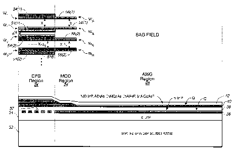
Reference is now made to Fig. 10 illustrating the selective area growth or SAG
mask set
employed over the wafer for forming the multiple active regions for both the
DFB regions 24
and the MOD regions 26, in particular, in the fabrication of TxPIC chips 30.
SAG is well
established in the art and comprises the employment of masks for both active
device regions
24 and 26 as shown in Fig. 10. The mask comprises pairs of Si02, Si3N4, or
other such mask
stripes 54, 56, etc., one set for each active region device, i.e., mask sets
54(1), 54 (2), etc.
across the DFB region 24 and mask sets 56(1), 56(2), etc. across the MOD
region 26. These
mask pairs form a space between the mask stripes that constitutes the growth
area or layer. As
the mask width, such as widths W1, W2, etc., and WA, WB, etc., are
sequentially made larger
as, for example, the masking openings X, X-A1, etc., and Y, Y-81; etc. become
sequentially
smaller, so that the growth rate of the semiconductor layer formed within the
mask openings
between pairs of mask stripes becomes larger.
Monotonic increase, itself, of the mask widths will render the deposited
material bandgap
to be narrower and, correspondingly, the operating wavelength of formed
regions in the mask
openings become progressively longer. Monotonic decrease, itself, of the
openings between
mask pairs will render the bandgap narrower and, correspondingly, the
operating wavelength
of the formed regions in the mask openings become progressively longer. The
decrease in
bandgap occurs as a result of both enhanced In concentration and enhance
growth rate in the
CA 02463522 2010-09-13
18
mask openings. Thus, a combination of monotonic increasing of mask widths with
a
monotonic decrease in mask set openings will provide a monotonic decrease in
bandgap and,
correspondingly, the operational wavelength of formed regions in the mask
openings will
monotonically increase along the plurality of mask set openings. It is best
that both of these
parameters are monotonically changed together to progressively increase the
operational
wavelengths across the arrays of DFB lasers and MODs because either too large
of a mask
width or a too narrow width of mask set openings by themselves will not
successfully achieve
the desired wavelength grid across the arrays. However, with a properly
designed simulation
program, the progression of designed and set wavelengths of the fabricated DFB
array can be
achieved to match the operational wavelengths of a standardized wavelength
grid, such as the
ITU grid. Note that the operational wavelength of the DFBs is governed by a
number of other
factors in addition to the bandgap and thickness of the SAO region, including
the grating
pitch, composition and duty cycle as well as the ridge-waveguide width and
etch depth.
However the SAO bandgap and thickness are two of the larger factors that
determine the
operational wavelength of the DFB. After TxPIC chip fabrication, any necessary
changes to
operational wavelengths of any of the respective DFB laser sources in the TxIC
array can be
adjusted or tuned by changes in the laser operating current or applied bias
and/or changes in
the laser operating temperature as described in more detail in Canadian Patent
Application No. 2,463,500.
It should be noted that other combinations can be utilized relative to the
monotonic
progression in changes of mask widths and/or mask openings. For example, the
mask
openings can be made progressively or monotonically larger (X, X+A1, X+4 ,
etc., and Y,
Y4-81; X+&2, etc.) across the DFB/MOD arrays and/or the mask widths can be
made
monotonically smaller (e.g., WI>W2>W3, etc, and WA>WB>WC, etc.).
The dN, the center pitch of the active region mask pairs, as illustrated in
Fig. 10, may be in
the range of 100 m to about 500 pm, preferably about 200 pm to about 350 pm.
Furthermore, the In/Ga or In/Al ratio increases as the mask widths WI... WN
and WA... Wm
become monotonically larger. This is because the growth source materials
diffuse laterally
along the surface of the SiO2 mask and laterally in the MOCVD gas phase over
the mask and
as the mask width becomes larger, the amount of such lateral diffusion becomes
larger,
providing more deposited material, in particular, In, in the mask opening and
forming a
thicker deposited layer and, correspondingly, the bandgap becomes smaller. In
this
connection, it should be noted that In molecules in the gas phase during MOCVD
processing
diffuse more rapidly, laterally across the mask than do Ga or Al molecules.
So, as the
CA 02463522 2004-04-07
WO 03/032036 PCT/US02/32113
19
thickness of quantum wells formed in active region 40 becomes larger due to
monotonically
increasing of mask widths (or, for that matter, also due to the monotonically
decreasing of
mask openings), the lattice distortion (compressive strain) becomes larger and
the transition
energy of the well becomes smaller. Furthermore, the bandgap becomes smaller
which is
dictated by the In/(Al+Ga) ratio.
In summary, then, SAG is a process where different widths of paired mask
stripes and
different opening widths between the pair of mask stripes change the thickness
of the Group
111-V alloy composition deposited in the mask openings thereby changing the
bandgap of the
as-grown compound formed in the array of mask openings. The thicker the as-
grown SAG
layer, the more In that is deposited into the mask opening which means a
longer wavelength
material.
Changes in the thickness of the various active regions (wells and barriers)
grown for an
array of active devices having progressively varying mask widths and/or
openings for growth
provides for varying thickness and bandgaps forming a series of progressively
wavelength-
shifted active regions capable of generating different lasing wavelengths
which can be
selectively provided to be within a standardized wavelength grid. The pairs of
mask sets for
MOD region 26 have progressively increasing widths as well as openings Y, Y-
81..., designed
to have the layers in region 26 to have smaller thicknesses with larger
bandgaps (shorter
wavelengths) for transparency to DFB generated light. As a specific example,
the core
bandgap of the Q core 40 in the DFB region 24 for the longest operational
wavelength may
correspond to about 1.58 m whereas, in this case, in the MOD region 26 may be
a core
bandgap corresponding to about 1.52 m, and in the case of the field of AWG
region 28 may
have a core bandgap corresponding to about 1.38 m. In the field region of the
mask where
the AWG is fabricated, the bandgaps are further larger for the same region.
Thus, a feasible
SAG budget is limited to a range of selective bandgaps achievable within the
constraints of
the widths of the mask surfaces, W1, W2, WA, WB, etc. and their opening
spacing X, X-z\1,
etc., Y, Y-81, etc as well as those governed by the limits of the strain /
thickness that can be
accommodated in the crystal. The inclusion of additional active or passive
optical
components, such as, an array of SOAs, puts further constraints on the SAG
budget. Thus, it
can be seen that if SAG budget can be reserved for bandwidth in the formation
of additional
channel wavelengths on a TxPIC chip, this provides for more effective cost
savings in the
manufacture and sale of a TxPIC module for use by carrier service providers.
Also, the
process control and yield of a TxPIC may be improved by a design that does not
require the
maximum attainable SAG budget to be utilized.
CA 02463522 2011-06-14
To be noted is that the SAG budget is extended into the field of the AWG. This
will also
limit the SAG budget. In the ideal case, the quantum wells in DFB region 24
are compressively
strained. But, at best, in a design that utilizes a single SAG growth to
deposit the core active/passive
waveguide regions, i.e., core 40, including AWG region 28, the modulator
quantum wells in core 40
5 will likely be untrained or heavily tensely strained which means, in the
context of this description,
unstrained, slightly tensile strained or slight compressively strained, such
as within a range of about
<+ 2,000 ppm strained from the lattice constant. As a result, it is difficult
to achieve, within the
SAG budget and process, a tensile strained modulator active region 26 between
a tensile strained
AWG waveguide region 28 and a DFB compressively strained active region 24. If
EA modulator
10 quantum well region 26 is not tensile strained, there is a constraint on
the EA modulator
performance relative to chirp, extinction ratio and insertion loss. This
desired balance in strain
between the three different regions can be made easier by the provision of an
additional growth step
in forming the waveguide core 40 in AWG region 28 from the growth step
employed to prepare the
SAG growth for the quantum well active regions 24 and 26 of the DFB and
modulator arrays. This
15 also enhances the SAG budget for the design of the bandgaps to be utilized
in the latter active
regions, i.e., the range is extended for additional SAG grown layers of
different bandgap.
In connection with the foregoing discussion, reference is made to Figs. 11-13
showing
another embodiment where there are additional processing steps of an etchback
andepitaxial
regrowth over AWG region 67 in order to provide relief in distributed strain
among the
20 DFB/MOD/AWG regions so that waveguide core through these regions may be
desirably left with
the most preferred structure for optimized performance in the MOD region 65,
which may optimally
consist of being tensile strained, or nominally strained compensated. TxPIC
comprises the epitaxial
growth on InP:Fe or n-InP substrate 62, n-lnP buffer layer (not shown),
followed by n-InP
confinement layer 64 and a grating layer 66. At this point, as in the case of
the previous
embodiment, the first epitaxial growth is complete and a DFB grating 167 is
formed in DFB region
63 across the chip. This is followed by the second epitaxial growth comprising
planarization layer
68, followed by deposition of a SAG mask and a subsequent epitaxial deposition
of the Q core or
active waveguide region 70 comprising multiple quantum wells and barriers of
1nGaAsP or
AlInGaAs (including quantum confinement layers), followed by NID-InP layer 72.
Note that in this
case, the amount of SAG shift required is significantly reduced as the SAG is
utilized to SAG shift
wavelength across the array as well as the SAG shift between the DFB and
modulator. The former
shift is typically about 15 to 30 nm and the latter shift is approximately 30
to 70 nm. The SAG shift
CA 02463522 2010-09-13
21
across the AWG may be about 150 nm. Thus, the requisite SAG shift is
approximately 45 to
100 nm. This is substantially smaller than the SAG shift of the device of Fig.
7 wherein shifts
greater than 200 nm are typically required Although it provides a very
convenient and useful
means of shifting the composition and thickness of the quantum. wells, SAG
makes control of
the composition and thickness of the material deposited around the mask
regions more
difficult. This difficulty increases with the amount of SAG shift. Thus, a
structure with
minimal SAG shift is desired to maximize composition and thickness variations
in the DFB
and MOD regions. This is essential to maximize MOD performance and yield as
well as to
control the DFB wavelength across the array. During the SAG epitaxial growth
step (the
third epitaxial growth step in this embodiment), the appropriate strain
requirements, relative
SAG growth and mask set openings and mask widths, are imposed only at DFB
region 63 and
MOD region 65 with disregard of the bandgap requirements for AWG region 67.
This is
because the core region 70 in region 67 will be later removed. Thus, the
requirements for
strain and bandgap budget can be limited to the growth of core 70 in the DFB
and MOD
regions 63 and 65. In the preferred case, the Q core 70 in DFB region 63 is
compressively
strained whereas, in the MOD region 65, the core 70 is slightly compressively
strained,
lattice-matched or tensely strained. At this time, a selective etch is
performed over region 67
to remove Q core layer 70 and InP layer 72 in that region. The depth of the
etchback is
minimized to limit the amount of later regrowth. As shown in Fig. 11, the
etebback may
extends at 69 into plauarization layer 68 but this depth is minimized.
Alternatively, a stop
etch may be utilized so as to not etch into the planarization layer. The
etchant employed may
be a wet or dry etchant as known in the art. As an example, the depth and
regrowth of layers
70 and 72 may be a thickness around 2,000 angstramns. Then, epitaxial growth
is, again,
reinitiated, i.e., the fourth epitaxial growth, comprising AWG core 73 of for
example,
InGaAsP or A]InOaAs followed by deposition of NID-InP layer 75. The regrowth
is taken up
to the edge 79 of MOD region 65 forming optical butt coupling 71 of waveguide
cores 70 and
73. An advantage of growing the waveguide core via this technique is that the
waveguide
core may be composed of bulk Q material. (as opposed to QW material as in the
embodiment
of Fig. 7). As a result, the refractive index (average bandgap) and thickness
of the core of the
waveguide of the AWG layer are easier to control resulting in improved
performance and
yield of the AWG.
The fiffi epitaxial. growth step includes an optional NID InP stop etch layer
74, an
optional Q rib-loading layer 76, a p-loP, thick confinement layer 78 and a p}`-
InOxaAs contact
layer 80. The optional stop etch layer may also be NID AAnAs, In.AWa.As,
InAtAsp or
CA 02463522 2004-04-07
WO 03/032036 PCT/US02/32113
22
InAlGaAsP. Q rib-loading layer 76 is optional as the preferred embodiment has
a ridge
waveguide structure.
As in the case of the embodiment in Fig. 7, the region of contact layer 80 and
the p-InP
confinement layer 78 over AWG region 67, as defined by region 78B to point or
position 84,
are etched back to rib-loading layer 76. This is followed by the sixth and
final epitaxial
growth step comprising the growth of NID-InP confinement layer 78B for the
reason
previously discussed in connection with the embodiment of Figs. 7-9.
To be noted is the butt joint 84 formed between p-InP layer 78A and NID-InP
layer 78B is
preferably displaced longitudinally relative to butt joint 71 formed at the
active/passive
waveguide core 70 at MOD/AWG interface 79, i.e., they are not vertically
aligned on top of
one another. This separation in vertical alignment prevents double reflections
of the
propagating mode from the joints as occurs in the case where these butt joints
are vertically
aligned. As an example, the displacement of the respective butt joints 71 and
84 may be in the
range of about 200 m to about 500 gm.
In addition the butt-joint formed in Fig. 11, it is possible to couple the
light emanating
from the modulators via an evanescent waveguide. This evanescent waveguide may
then be
patterned to form a wavelength selective combiner such as an AWG.
Alternatively, a second technique to form a similar structure as described in
Fig. 11 is to
perform the first thru third epitaxial growths (and processing associated with
them) as
described above. After the third growth step, the layers 74-80 are grown in a
fourth growth
step to complete the active devices. Subsequently, the material over the AWG
region is
etched and removed via a deep etch that stops or extends slightly into layer
69. This is
followed by a single growth for the core waveguide of the AWG and the NID-InP
layer 78B.
This method is preferred over the previous described approach in that it
requires one less
regrowth and only has a single butt-joint at the AWG / MOD interface. However,
this method
also has the disadvantages of. requiring a precise deep etch prior to the AWG
growth, difficult
alignment of the optional Q rib-loading layers and AWG core waveguide layers
across the
butt-joint interface, and potential significant runaway (enhanced) growth at
the butt joint
interface. Thus, careful control of processing techniques is required.
The rib loaded waveguides 69 and 71 are then formed by selective etchback of
the active
and passive components, as seen in Figs. 12 and 13. A dry-etch is performed
that stops at stop
etch layer 74. If no stop etch layer 74 is present in the structure, the etch
depth must be
precisely controlled. For the ultimate optimization of performance and yield
of the
components on the TxPIC, it may be desirable to etch the ridges in each of the
sections to
CA 02463522 2004-04-07
WO 03/032036 PCT/US02/32113
23
different widths and depths as described previously. This may be accomplished
by etching all
elements to the shallowest required depth for a given element, followed by
masking the
element and selective etching at desired width to the desired depth. This
process is repeated
as many times as necessary to achieve optimal etch depths in the different
elements.
Ridge waveguide performance for this and the previous embodiment for both
active and
passive optical components are strongly dependent on ridge height.
Furthermore, the ridge
sidewall angle and angle control are critical as well. The TxPIC embodiments
described
herein have waveguides which are curved and hence span multiple crystal
planes.
Consequently, it is desirable to utilize anisotropic dry etching with minimal
crystallographic
etching that occurs when utilizing wet etches when forming the ridge
waveguides.
Additionally, it is important to stop, at a precise depth, when defining the
ridge waveguides in
order to control the mode size, and hence optical confinement in the
waveguides. This is
typically accomplished via stop etch layer 42 and 74, such as, for example,
InGaAsP, that is
used in conjunction with a wet etch. However, in the case of the embodiments
here, the
routing of the waveguides in, out and through the multiplexer, such as in the
case of an AWG,
requires the waveguides to bend and thus span multiple crystal planes.
Virtually all wet
etches have some crystallographic dependence, making the employment of such an
etching
method, as applied to a TxPIC chip described herein, unpractical because the
resulting ridge
waveguides will vary in width across the chip. Thus, a stop etch layer that
facilitates an etch
stop with dry etching will significantly improve the control and
reproducibility of the process.
Potential stop etch layers 42 and 74 for dry etching, e.g., CH4/H2, are
InAlAs, InAlGaAs,
InAlAsP and InAlGaAsP. The key in all of these stop etch layers is to have as
high an Al
content as possible. Furthermore, additional P to the Al-bearing stop etch
compound should
further improve etch selectively (or stopping power). It is not required for
the stop etch layer
to be lattice matched (e.g., tensile strained InAlAs with higher Al
composition than lattice
matched InAlAs is preferred).
As previously discussed, the ridge waveguide is desired so the propagating
mode in the
various waveguide paths formed on the TxPIC chip experience lower confinement
which
enhances the intensity output from the DFB and MOD, helping to eliminate the
need for
providing any on-chip amplification, such as SOAs.
Distinctive advantages of employing a waveguide core butt joint 71, as shown
in Fig. 11,
is that this joint permits higher performance (e.g., power output, chirp,
extinction ration and
insertion loss) from the DFB/MOD regions 63 and 65 since there is better
control in achieving
the desired strain for MOD region 65. Also, in deploying a separate epitaxial
growth for
CA 02463522 2004-04-07
WO 03/032036 PCT/US02/32113
24
AWG region 67, the Q waveguide cores 71 formed in the. AWG region will have a
more
uniform bandgap and allow independence and flexibility in the design and
growth of the DFB
quantum well active region formed in separate core waveguide 70. While such
butt joints do
have a certain amount of insertion loss due to light reflections and
scattering at the joint,
careful control of the epitaxial growth processes can maintain these losses
low.
As a still further note, the use of the Q comprising InAlGaAs in the active
region/waveguide core 40 and 70 in TxPICs 30 and 60 formed via SAG processing
across the
TxPIC chip, in lieu of InGaAsP, provides for better bandgap uniformity, a
better DFB laser
due to better optical confinement and better modulator performance due to
reduced hole "pile-
up" in the valence band. The better uniformity of InAlGaAs is achieved
principally due to the
lack of P in the quaternary compound. The cracking temperature of PH3 is
sufficiently
different than other constituents for this quaternary in the MOCVD process
that it is difficult
to achieve high compound uniformity of InGaAsP particularly over a large
surface area. Also,
such an Al-bearing layer provides for increased interface abruptness of the
quantum well
interfaces.
Also, it is within the scope of the embodiment of Figs. 11-13 that InAlGaAs
active/passive
waveguide core 70 be initially grown across the DFB/MOD/AWG regions while the
waveguide core 73 of AWG region 67 be etched and then regrown as InGaAsP or
InAlGaAs.
The layers grown sequentially in AWG region 67 are preferably bulk layers,
i.e. an AlInGaAs
layer, in lieu of multiple Q quantum well and barrier layers, to minimize any
non-uniformity
induced by quantum-size effects.
It should be noted that in connection with EA modulators in MOD regions 26 and
65 in
the two discussed embodiments, at least a double quantum well stack (e.g.,
double quantum
well with n number of repeats) is one approach to achieving high performance
operation. For
long optical transmission spans, a TxPIC chip with EA modulators that possess
negative chip,
low insertion loss and high extinction ratio is desired. In order to realize
this with the full
SAG processing of a TxPIC (while maintaining the constraints imposed by the
SAG budget),
a double-quantum well structure is preferred for the EA modulator. Preferably,
the active
region of the EA modulators includes at least two different regions where the
potential well of
a first region is deeper than that of a second region. This preference arises
from the fact that it
is not possible to achieve the requisite tensile stain in the modulator region
for optimal
performance in a single well structure for a TxPIC chip with full SAG
processing of the
active/passive waveguide. The double well structure provides the ability to
achieve good
negative chirp characteristics, extinction ratio, and insertion loss without
the utilization of
CA 02463522 2004-04-07
WO 03/032036 PCT/US02/32113
significant strain (e.g., < +/-2000 ppm strain). Each of these regions can be
a composite of
several layers, i.e., pairs of quantum wells and barriers, but a key factor is
that the average
electron potential of the first region should be less than that of the second
region. Generally,
also the thickness of the first region is greater than or equal to that of the
second region,
5 although in all of the embodiments to be discussed, which are shown in Figs.
14A-14H, the
thickness is shown to be greater in the first region. Figs. 14A to 14H
illustrate the valence
band for various combinations of such first and second region active regions.
The Q material
regime is InGaAsP or AlInGaAs.
As shown in Fig. 14A, modulator stepped quantum well region 90 comprises a
first step
10 91 and a second step 92 where the potential well of the first step 91 is
deeper than the
potential well of the second step 92, and the thickness of the first step 91
is greater than the
thickness of the second step 92. The quantum well steps 91 and 92 may be
separated by a
barrier 93, as shown in dotted outline at 93 in Fig. 14A, which may also be
multiple barrier
layers instead of one barrier. Barrier 93 provides for delineation between the
two well steps
15 91 and 92 to help confine the electron or hole in either well step of the
dual well step structure
where the peak of the probability density function shifts from the first step
region to the
second step region of the structure upon application of a reverse bias. This
is true for the
barrier or barriers illustrated in each of the remaining Figs. 14B-14H.
In Fig. 14B, modulator stepped quantum well region 94 comprises a first
quantum well
20 step 95 and a second quantum well step 96 where the latter is graded and
the former is flat. A
barrier layer 96 may be formed between well steps 95 and 96.
In Fig. 14C, in modulator stepped quantum well region 98, both well steps 99A
and 99B
are index graded with a vertical step 100 provided between the well steps. A
barrier layer 96
may be formed between wells 99A and 99B. The well step 99A is thicker and
deeper than
25 well step 99B.
In Fig. 14D, modulator stepped quantum well region 102 comprises a first well
step 103
and a second well step 104 where the first well step 103 is graded and the
second well step
104 is flat. A barrier layer 105 may be provided between well steps 103 and
104.
In Fig. 14E, modulator stepped quantum well region 106 comprises a first well
step 107
and a second well step 108 where the well steps are both graded with the first
well step 107
being deeper and equal to or thicker than the second well step 108. A barrier
layer 109 may
be provided between well steps 107 and 108.
In Fig. 14F, modulator stepped quantum well region 110 comprises a first well
step 111
and a second well step 112 where both well steps are at the same well
potential with the first
CA 02463522 2004-04-07
WO 03/032036 PCT/US02/32113
26
well step 111 being thicker than the second well step 112. Also, a barrier
layer 110 is
provided between well steps 111 and 112.
The modulator quantum well region 114 in Fig. 14G is similar to that in Fig.
14F except
that the well potentials are not the same. Modulator stepped quantum well
region 114
comprises a first well step 115 and a second well step 117 where the first
well step 115 has a
deeper well potential than the second well step 116 and, also, the first well
step 115 is thicker
than the second well step 116. Also, a barrier layer 117 is provided between
well steps 115
and 116.
In Fig. 14H, modulator stepped quantum well region 118 comprises a first well
step region
119 having a plurality of bandgap steps 122 and a second well step region 120
having a
plurality of bandgap steps 123. The steps in regions 119 and 120 increase
monotonically
where first step region 119 is thicker than the step region 120 and, further,
has on average a
lower conduction band energy for region 119. Also, one or more barriers 124
and 125 may be
provided at the edge of well steps 123 of the second well step region 120 as
illustrated in Fig.
14H.
It should be noted that there are many possible alternative configurations and
these
illustrations in Figs. 14A-14H illustrate just a few. A key point is that the
active region
includes at least different regions in a stepped quantum well where the
potential well of a first
step or region is deeper than that of a second step or region where the
average electron
potential of the first step or region should be less than that of the second
step or region. The
stepped quantum well active region advantageously requires a lower applied
electric field to
split the electron-hole exciton as well as providing negative chirp with high
extinction ratio
and minimized insertion loss compared to a single well active region.
It should be noted that additional multiple well steps can be formed in each
of the two
steps or regions of the embodiments of Figs 14A-14G as is illustrated in Fig.
14H.
A complex-coupled grating structure in the DFB arrays, as previously
described, may be
used in conjunction with the ridge-waveguide PIC structures described herein.
A complex-
coupled grating structure is provides more enhanced stability for high-power
operation and is
more immune to back reflections from within the TxPIC. This may be used
advantageously
with the TxPIC ridge waveguide structures described herein where different
ridge widths or
heights are utilized for various elements in the PIC. These different ridge
widths and heights
create an index step between elements which causes back reflection of the
propagating light to
the DFB. Similarly, the butt-joint(s) of the devices described in Figs. 7 and
11 also cause
back reflections. The complex-coupled grating DFB is more immune to these back
CA 02463522 2004-04-07
WO 03/032036 PCT/US02/32113
27
reflections, and thus, further facilitates high power operation. Also, the
complex-coupled
grating may be used in conjunction with a directly modulated laser, as in Fig.
1, to achieve
high power and improved chirp characteristics.
The utilization of complex-coupled gratings facilitates a high-performance EML
structure
that utilizes an identical active layer (IAL) approach. The IAL approach may
also be
deployed with a band-edge Mach-Zehnder modulator structures. Such IAL
approaches are
known in the art. See, for example the article of R. A. Salvatore et al,
"Electroabsorption
Modulated Laser For Long Transmission Spans", IEEE Journal of Quantum
Electronics, Vol.
38(5), pp. 464-476 May, 2002,. Such structures may be utilized advantageously
in the TxPIC
disclosed herein. The IAL EML does not require any bandgap shift between the
laser and the
modulator. Thus, the SAG budget is effectively improved for the TxPIC
structures of either
Figs. 7 or 11. In this structure, the only SAG that is required is to tune the
bandgap from
channel to channel. This requires the least amount of SAG (typically around 15
to 30 nm).
As a result of the small amount of SAG processing required, the uniformity of
the
composition and thickness of the material in the SAG regions (the IAL
elements) may be
significantly improved, yielding improved yields. Furthermore, the complex-
coupled grating
structure in combination with a ridge-waveguide structure facilitates high-
power operation.
Note that unlike that described in the above mentioned article of R.A.
Salvatore et al., the
ridge structure in the modulator in the approach here may be either a deep
ridge or a shallow
ridge. A deep-ridge is preferred for improved manufacturability and reduced
bias voltage, but
provides increased back reflection to the DFB. Furthermore, the AWG region may
be either a
deep or shallow ridge.
The complex coupling allows the greatest degree of design freedom for the
ridge
structures while being the most immune to back reflection. The IAL approach
may also be
used in conjunction with the full SAG approach. In this approach, the IAL
approach reduces
the SAG budget by about 50 nm. This facilitates a wider process window for the
SAG growth
as well as allowing for improved uniformity as the reduced SAG shift may
provide better
composition and thickness uniformity.
Note that other selective bandgap shifting techniques may also be employed to
vary the
wavelength across any of the elements in the PIC. These may be substituted or
utilized in
conjunction with any of the aforementioned SAG processing steps. These
selective bandgap
shifting techniques include disordering (also known as layer intermixing) or
multiple
regrowths (forming butt joints across the array or along a single channel).
Disordering may be
implemented by a variety of methods, including impurity-induced layer
disordering, vacancy-
CA 02463522 2004-04-07
WO 03/032036 PCT/US02/32113
28
enhanced layer disordering, or implantation (defect) enhanced layer
disordering. If
disordering is employed in the AWG or optical combiner region, it is
preferably does not
introduce significant impurities into the materials that form optical
waveguides. This
preference is dictated by the fact that impurities can act as optical
absorption centers,
increasing the propagation loss in the passive structure. Furthermore, care
must be taken to
ensure that dislocations are not introduced in the PIC materials during the
disordering process,
resulting in degraded performance and reliability. Note that any of the
aforementioned
bandgap shifting techniques may be used solely or in concert with each other
throughout this
invention. Specifically, these bandgap shifting techniques may be utilized in
the devices of
Figs. 1, 7, and 11 as well as in conjunction with any IAL structure in a
TxPIC.
Correctly targeting and maintaining the uniformity of the composition and
thickness of the
material in the DFB and MOD regions is essential to the performance and yield
of the TxPIC.
The utilization of any selective bandgap shifting technique, including SAG,
introduces further
error and uncertainty in the composition and thickness uniformity. Thus, it is
most desirable
to only shift the bandgap of the least number of elements in a TxPIC. The
wavelength of the
DFB is significantly affected by the grating pitch and stripe width.
Furthermore, the window
of acceptable operation of an EA modulator is typically on the order of about
5 to 10 nm.
Thus, for a TxPIC, it is not necessary to shift every channel with a bandgap
shifting technique.
Therefore, an embodiment of this invention is to only shift the composition
and/or thickness
every it" element in the PIC, wherein i > 1. In such cases for the DFB lasers,
a shift in the
wavelength is still accomplished with a composition and/or thickness shift
every ith laser.
While the invention has been described in conjunction with several specific
embodiments,
it is evident to those skilled in the art that many further alternatives,
modifications and
variations will be apparent in light of the foregoing description. Thus, the
invention described
herein is intended to embrace all such alternatives, modifications,
applications and variations
as may fall within the spirit and scope of the appended claims.