Note: Descriptions are shown in the official language in which they were submitted.
CA 02464139 2004-04-16
WO 03/058313 PCT/US02/34075
OPTICAL SYSTEM FOR CALIBRATION AND
CONTROL OF AN OPTICAL FIBER SWITCH
BACKGROUND OF THE INVENTION
1. Field of the Invention
The present invention relates to optical fiber cross-connect switching.
2. Description of the Related Art
As optical fiber progressively supplements and replaces metal wire as the
backbone of telecommunications networks, the switches that route optical
signals have
emerged as a significant bottleneck. Transmission systems move information as
optical
photons but the switching systems and so-called cross-connect fabrics that
switch, route,
multiplex, and demultiplex optical signals have generally been electronic.
Electronic
switching requires light to be converted to an electronic signal to pass
through the switch
and then be reconverted to light in a process termed optical-electronic-
optical (OEO)
conversion that introduces both time delay and cost.
There is great interest in the telecommunications industry, therefore, in
developing all optical switching to avoid the necessity of multiple OEO
conversions. As
described, for example, by Bishop et al. in Scientific American (January,
2001, pp. 88-
94), all optical switches based on a number of underlying technologies
including Micro
Electro Mechanical Systems (MEMS) tilting mirrors, thermo-optical devices,
bubbles
formed by inkjet printing heads, and liquid crystals, have been proposed.
Optical fiber
switches based on MEMS mirrors are particularly attractive because they can
incorporate
very large scale integrated circuits and can be robust, long-lived, and
scalable.
An optical fiber switch described in U.S. Patent 5,960,132 to Lin, for
example,
includes an array of hinged MEMS mirrors, each of which can be rotated about
its hinge
between a reflective state and a non-reflective state. An array of N2 such
mirrors is
required to switch signals carried by N input optical fibers from one to
another of N
output optical fibers. Unfortunately, N2 scaling results in unmanageably
complex devices
for large N.
Another optical fiber switch described in Bishop et al., cited above, as well
as in
Bishop et al., Photonics Spectra (March 2000, pp. 167-169) includes an array
of MEMS
mirrors disposed on a single surface. Each mirror tilts independently to
direct light
received from an array of input/output optical fibers to any other mirror and
thus to any
CA 02464139 2004-04-16
WO 03/058313 PCT/US02/34075
input/output fiber. This optical fiber switch does not appear to include
optical diagnostics
which would enable active closed-loop optical feedback control of the mirror
orientations
or allow input presence detection.
Optical fiber switches having a low insertion loss and capable of cross-
connecting
large numbers of input and output fibers would further the development of
fiber optic
telecommunications networks.
SUMMARY
The present invention provides methods of calibrating and operating optical
switches. A method of calibrating an optical switch including a first port, a
second port,
a first mirror and a second mirror in accordance with the present invention
includes
directing a first control beam of light onto the first mirror and directing a
second control
beam of light onto the second mirror. The method also includes controlling ari
orientation of the first mirror such that the first mirror reflects the first
control beam of
light to a predetermined position on a first position sensing detector, and
controlling an
orientation of the second mirror such that the second mirror reflects the
second control
beam of light to a predetermined position on a second position sensing
detector. A third
beam of liglit (e.g., at a telecommunications wavelength) incident on the
first inirror from
the first port is thereby directed to the second mirror and thence to the
second port.. The
method further includes controlling the orientations of the first mirror and
the second
mirror to maximize the intensity of the third beam of light coupled into the
second port,
and recording signals determined from outputs provided by the first and second
position
sensing detectors.
In one implementation, the calibration method further includes controlling the
orientations of the first and second mirrors to minimize a reflection of the
third beam of
light from, for example, the second port. The calibration method may also
include
directing a third control beam of light (fourth beam) onto a third position
sensing detector
via the first mirror and the second mirror, and recording a signal determined
from outputs
provided by the third position sensing detector.
This calibration method, which is typically performed only once in the factory
after assembly of the optical switch, allows highly accurate control of the
mirrors in the
optical switch during subsequent switching operations in the field.
-2-
CA 02464139 2004-04-16
WO 03/058313 PCT/US02/34075
A method of operating an optical switch including a first mirror and a second
mirror in accordance with an embodiment of the present invention includes
directing a
first control beam of light onto the first mirror, and controlling an
orientation of the first
mirror such that the first mirror reflects at least a portion of the first
control beam of light
to a predetermined position on a first position sensing detector. The method
also includes
directing a second control beam of light onto the second mirror, and
controlling an
orientation of the second mirror such that the second mirror reflects at least
a portion of
the second control beam of light to a predetermined position on a second
position sensing
detector. The method further includes directing a third control beam of light
onto the
second mirror via the first mirror, and controlling an orientation of the
first mirror, of the
second mirror, or of both mirrors such that at least a portion of the third
control beam of
light is directed to a predetermined position on a third position sensing
detector. In one
implementation, an orientation of at least one of the first and second mirrors
is controlled
with an angular resolution better than about 0.005 .
The first, second, and third predetermined positions referred to in the
operation
method may be determined, for example, by the calibration method described
above.
The first, second, and third control light beams utilized in the operation
method
are separate from the light beams being routed through and switched by the
optical
switch. Hence, the mirrors in the optical switch can be aligned to couple
signal (e.g.,
telecommunications) light beams input through particular input ports to
particular output
ports before those signal light beams are provided to the optical switch.
Moreover, the
orientations of the mirrors may be controlled without sampling the signal
light beams,
thus reducing the insertion loss of the optical switch.
The present invention also provides optical switches in which the orientations
of
mirrors are measured and controlled using control light beams and position
sensing
detectors. In one embodiment, an optical switch includes a plurality of
mirrors, a light
source located to illuminate the plurality of mirrors, a plurality of position
sensing
detectors, and an imaging system located to image the plurality of mirrors at
an image
plane spaced apart from the detectors. Signals provided by the position
sensing detectors
correspond to orientations of corresponding mirrors. This arrangement allows
the
orientations of the plurality of mirrors to be measured and controlled with,
for example, a
resolution of better than about 0.04 over a range of greater than about 20
(about 9 bit
accuracy).
-3-
CA 02464139 2007-08-13
In another embodiment, an optical switch includes a first mirror, a second
mirror, a light source, and a position sensing detector located to detect
light output by
the first light source and reflected by both of the first mirror and the
second mirror.
A signal provided by the detector corresponds to the orientations of the first
mirror
and the second mirror. This arrangement allows the orientations of the first
and
second mirrors to be measured and controlled with, for example, a resolution
of
better than about 0.005 over a range of greater than about 0.15 (about 5 bit
accuracy). If the optical switch also includes light sources, imaging systems,
and
position sensing detectors as described in the previous embodiment, then the
orientations of the mirrors may be measured and controlled with, for example,
a
resolution better than about 0.005 over a range of greater than about 20
(about 12 bit
accuracy).
In another embodiment, an optical switch includes a first plurality of
mirrors,
a second plurality of mirrors, a light source and a plurality of position
sensing
detectors. Each detector is located to detect light output by the light
source, reflected
by one of the first plurality of mirrors, and reflected by one of the second
plurality of
mirrors. Signals provided by the detectors correspond to the orientations of
the first
plurality of mirrors and the second plurality of mirrors. In one
implementation, the
orientations of the mirrors in the first and second pluralities of mirrors are
measured
and controlled with a resolution of better than about 0.005 over a range of
greater
than about 0.15 (about 5 bit accuracy). If the optical switch also includes
light
sources, imaging systems, and position sensing detectors as described above,
then the
orientations of the mirrors may be measured and controlled with, for example,
a
resolution better than about 0.005 over a range of greater than about 20
(about 12 bit
accuracy).
The high resolution control of mirror orientations achievable in optical
switches provided by embodiments of the present invention reduces the
insertion loss
of the optical switches. Consequently, optical fiber switches may be
controlled in
accordance with embodiments of the present invention to cross-connect more
than a
thousand input ports to more than a thousand output ports with an insertion
loss of
less than, for example, about 3 decibels.
4
CA 02464139 2007-08-13
In one aspect, the present invention provides an apparatus, comprising: an
optical switch having: a first mirror to receive a first light beam and to
reflect the first
light beam to a predetermined position on a first position sensing detector; a
second
mirror to receive a second light beam and to reflect the second light beam to
a
predetermined position on a second position sensing detector, wherein the
first and the
second position sensing detectors are arranged as a substantially planar
array; a control
system to control a first orientation of the first mirror, the first mirror to
reflect the first
light beam to a predetermined position on a first position sensing detector in
response to
the orientation, the first mirror to receive a third light beam and to direct
the third light
beam received fi-om a first port to the second mirror in response to the frst
orientation,
the control system to control a second orientation of the second mirror, the
second mirror
to reflect the second light beam to a predetermined position on a second
position sensing
detector in response to the second orientation, the second mirror to direct
the third light
beam to a second port to the second mirror in response to the second
orientation, the first
and the second orientations to maximize an intensity of the third light beam
coupled into
the second port, the control system to record signals output from the first
and second
position sensing detectors; and an aperture plate substantially parallel to
and spaced apart
from said array by about 0.5 to 1.0 millimeters.
In another aspect, the present invention provides an apparatus, comprising: an
optical switch having: a first mirror to receive a first light beam and to
reflect the first
light beam to a predetermined position on a first position sensing detector; a
second
mirror to receive a second light beam and to reflect the second light beam to
a
predetermined position on a second position sensing detector; a first light
source; a
second light source, wherein said first light source and said second light
source each
output pulses of light such that pulses of light output by said first light
source do not
substantially overlap in time at said position sensing detectors with pulses
of light output
by said second light source; and a control system to control a first
orientation of the first
mirror, the first mirror to reflect the first light beam to a predetermined
position on a first
position sensing detector in response to the orientation, the first mirror to
receive a third
light beam and to direct the third light beam received from a first port to
the second
mirror in response to the first orientation, the control system to control a
second
orientation of the second mirror, the second mirror to reflect the second
light beam to a
4a
CA 02464139 2007-08-13
predetermined position on a second position sensing detector in response to
the second
orientation, the second mirror to direct the third light beam to a second port
to the second
mirror in response to the second orientation, the first and the second
orientations to
maximize an intensity of the third light beam coupled into the second port,
the control
system to record signals output from the first and second position sensing
detectors.
BRIEF DESCRIPTION OF THE DRAWINGS
Figure 1 is a schematic illustration of an optical switch in accordance with
an
embodiment of the present invention.
4b
CA 02464139 2004-04-16
WO 03/058313 PCT/US02/34075
Figure 2 is a schematic illustration of an optical switch in accordance with
another
embodiment of the present invention.
Figure 3 is a schematic illustration of an optical switch including input and
output
sensors in accordance with an embodiment of the present invention.
Figure 4 is a schematic illustration of an optical switch including monitor
channels in accordance with an embodiment of the present invention.
Figure 5 is a schematic illustration of optical paths of control light beams
in an
optical switch in accordance with an embodiment of the present invention.
Figure 6 is a schematic illustration of optical paths of control light beams
in an
optical switch in accordance with another embodiment of the present invention.
Figure 7 is a schematic illustration of optical paths of control light beams
in an
optical switch in accordance with another embodiment of the present invention.
Figure 8 is a schematic illustration of optical paths of reference light beams
in an
optical switch in accordance with an embodiment of the present invention.
Figure 9 is a schematic illustration of optical paths of reference light beams
in an
optical switch in accordance with another embodiment of the present invention.
Figure 10 is a schematic illustration of optical paths of reference light
beams in an
optical switch in accordance with another embodiment of the present invention.
Figure 11 is a timing diagram showing the relative timing of light pulses
provided
by three lasers in accordance with an embodiment of the present invention.
Figure 12 illustrates, in a flow chart, a method of calibrating and aligning
an
optical switch in accordance with an embodiment of the present invention.
Figure 13 illustrates, in a flow chart, a method of operating an optical
switch in
accordance with an embodiment of the present invention.
Figure 14 illustrates, in a flow chart, a method for recalibrating an optical
switch
in accordance with an embodiment of the present invention.
Figure 15 illustrates, in a block diagrani, relationships between mirror
arrays, light
sources, and position sensing detectors in an optical switch in accordance
with an
embodiment of the present invention.
Like reference numbers in the various figures denote same parts in the various
embodiments. Dimensions in the figures are not necessarily to scale.
-5-
CA 02464139 2004-04-16
WO 03/058313 PCT/US02/34075
DETAILED DESCRIPTION
An optical fiber cross-connect switch in accordance with embodiments of the
present invention routes light input through any one of N input ports to any
one of P
output ports. In a typical optical path through a switch, light entering the
switch through
an input port is incident on a corresponding first micro-mechanical mirror in
a first two
dimensional array of micro-mechanical mirrors. The first micro-mechanical
mirror,
which can be oriented in a range of arbitrary directions (d0,dcp), is tilted
to direct the light
to a second micro-mechanical mirror in a second two dimensional array of micro-
mechanical mirrors. The second micro-mechanical mirror, which can also be
oriented in
a range of arbitrary directions (d0,d(p), is tilted to direct the light to a
corresponding
output port and hence out of the switch.
The light may be switched from the output port to which it is initially
directed to
another output port by reorienting the first micro-mechanical mirror to direct
the light to a
third micro-mechanical mirror in the second array of micro-mirrors, and
orienting the
third micro-mechanical mirror to direct the light to its corresponding output
port. A
control system is provided to control the orientations of the micro-mechanical
mirrors
and thus accomplish the switching. A number of embodiments will be described
in
which the orientations of the various micro-mechanical mirrors are measured
and
controlled by reflecting light beams (separate from those being routed through
and
switched by the optical fiber switch) from the micro-mechanical mirrors and
measuring
the locations at which the reflected light beams are incident on position
sensing detectors.
Although the number of input ports equals the number of output ports (N = P)
in
the embodiments described below, in other embodiments N < P or N > P.
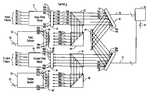
For convenience of illustration, an optical fiber cross-connect switch 2
(Figure 1)
in accordance with one embodiment will be described with reference to N = 5
input
optical fibers 4a-4e serving as input ports, P = N = 5 output optical fibers
6a-6e serving
as output ports, and N= 5 of various other optical elements and light beams
located in
optical paths between input fibers 4a-4e and output fibers 6a-6e, as shown in
Figure 1. It
should be understood, however, that in other embodiments in accordance with
the present
invention, N and P are both typically greater than about 1000. In one
embodiment, for
example, N is about 1200 and P = N.
As is conventional in Dense Wavelength Division Multiplexing, each of the
input
optical fibers may carry liglit having a plurality of wavelengths. In one
implementation,
-6-
CA 02464139 2008-12-15
the light carried by the input optical fibers has wavelengths near about 1310
nanometers (nm)
or about 1550 nm. The input optical fibers and the output optical fibers are,
for example,
conventional Coming, Incorporated SMF-28 single mode optical fibers having a
core
diameter of about 8 microns (gm) and a cladding diameter of about 125 m.
Other optical
fibers suitable for optical communications applications may also be used.
Referring to FIG. 1, N input optical fibers 4a-4e enter input fiber block 8,
which
rigidly positions their respective ends l0a-IOe in a two dimensional array at
surface 12 of
block 8. Surface 12 is polished, for example, to a flatness better than about
300 nanometers
(nm) to form a planar surface including fiber ends 10a-10e. Input fiber block
8 fixes the
positions and orientations of fiber ends 10a-10e with respect to other optical
elements in
optical switch 2, thereby preventing motion of fiber ends l0a-l0e from
misaligning switch 2.
In one implementation, input fiber block 8 includes a silicon plate through
which pass
N substantially parallel holes arranged, for example, in a rectangular array
having horizontal
and vertical pitches of about 1 millimeter (mm). Into each hole is inserted a
corresponding
one of input optical fibers 4a-4e. Surface 12 of input fiber block 8 is
polished to form a planar
surface substantially perpendicular to the input optical fibers and including
their ends l0a-
10e. At surface 12 the N optical fiber ends form, for example, a rectangular
array as
described above. For N=1200, for example, the array may be a rectangular
30×40 array.
Various implementations of input fiber block 8 are described in greater detail
in U.S. Patent
No. 6,480,320.
Light carried by input optical fibers 4a-4e is output as diverging cones of
light by,
respectively, the cores of fiber ends 10a-10e. The N lenslets (small lenses)
14a-14e of lenslet
array 14 collect light output, respectively, by fiber ends l0a-l0e and form,
respectively, N
substantially parallel or weakly focused light beams 16a-16e. Lenslet array 14
is located
adjacent to input fiber block 8, with lenslets 14a-14e arranged in a pattem
matching that of
fiber ends l0a-l0e such that lenslets 14a-14e are located with their optical
axes
approximately centered on, respectively, fiber ends IOa-10e.
In one implementation, lenslets 14a-14e have focal lengths of about 4 mm,
diameters of about 1 mm, and are spaced approximately 3 mm from surface 12 of
input
block 8. Lenslet array 14 is formed, for example, from fused silica, optical
glass,
silicon, plastic, or epoxy. Suitable lenslet arrays are available, for
example, from
Adaptive
-7-
CA 02464139 2008-12-15
Optics Associates, Inc. of Cambridge, Mass., Advanced Micro Optical Systems,
GmbH, of
Saarbrucken, Germany, and Corning Rochester Photonics Incorporated of
Rochester, N.Y.
Light beams 16a-16e formed by lenslets 14a-14e are incident on micro mirror
array
18. Micro mirror array 18 includes N micro mirrors 18a-18e positioned above
reference
surface 19 and arranged in a pattern, such as a rectangular array,
corresponding to the
patterns of fiber ends l0a-l0e and lenslets 14a-14e. The pitch of micro
mirrors 18a-18e, in a
direction along surface 19 parallel to a plane of incidence defined by one of
light beams 16a-
16e and an axis normal to surface 19 at the point at which the light beam
would intersect
surface 19, is elongated compared to the corresponding pitch of lenslets 14a-
14e such that
substantially parallel or weakly focused light beams 16a-16e are incident
approximately
centered on micro mirrors 18a-18e, respectively. The orientations of micro
mirrors 18a-18e
with respect to reference surface 19 are individually controllable over a
range of arbitrary
angles (d0,d(p) by control system 20 with electrical signals transmitted via
bus 22.
In one embodiment, micro mirror array 18 is a micro-electro-mechanical system
(MEMS) micro mirror array described U.S. Patent No. 6,480,320. In this
embodiment, micro
mirrors 18a-18e are freely rotatable micro-electro-mechanical mirrors actuated
by, for
example, electrostatic, electromagnetic, piezoelectric, or thermal actuation
means
incorporated into the micro mirror array. Other types of micro mirrors and
micro mirror
arrays may also be used. Control system 20 is, for example, an optical switch
control system
described in U.S. Patent No. 6,882,769 and U.S. Patent No. 6,614,954.
In one implementation, light beams 16a-16e are incident on micro mirror array
18 at
an angle of incidence of less than about 25 , as conventionally defined with
respect to an axis
normal to mirror array reference surface 19, and the footprints of light beams
16a-16e (beam
spots) on, respectively, micro mirrors 18a-18e are consequently nearly
circular. In this
implementation, the angles of incidence of the light beams on individual micro
mirrors may
vary, for example, from about 15 to about 35 . In other implementations, the
light beams
may be incident on micro mirror array 18 at an angle of incidence of, for
example about 0 to
about 60 .
-8-
CA 02464139 2004-04-16
WO 03/058313 PCT/US02/34075
The beams spots at the micro mirrors may have nearly uniform intensity or, for
example, an intensity that varies radially. One of ordinary skill in the art
will recognize
that the diameters of beam spots having radially varying intensities may be
defined in
standard manners depending on the form of the intensity distribution. For
example, the
diameter of a Gaussian beam spot having a radial distribution l(r) = I(0)exp(-
2(r/w)2) is
typically taken to be 2w.
In one implementation, the beam spots at the micro mirrors are nearly circular
with diameters of about 0.6 mm. Small, nearly circular beam spots allow the
use of
small, nearly circular micro mirrors 18a-18e. This is advantageous, as the
smaller the
micro mirror, the lower its inertia and the easier it is to move. In addition,
nearly
circular mirrors experience a more uniform stress from any coating applied to
them and
thus deform less than do similarly coated substantially noncircular mirrors.
Micro
mirrors 18a-18e are, for example, approximately elliptical with major and
minor
diameters of about 1.0 mm and 0.9 mm, respectively.
Micro mirrors 18a-18e reflect incident light beams 16a-16e, respectively, onto
fold mirror 24. Fold mirror 24 is, in one implementation, a conventional flat
gold coated
mirror highly reflective (> 98%) at infrared wavelengths including 1310 nm and
1550
nm. Such conventional gold coated mirrors may be obtained from many commercial
sources. In another implementation of the illustrated embodiment, fold mirror
24 is a flat
dichroic beam splitter that transmits about 30% to about 70%, preferably about
50%, of
incident light having a wavelength of about 600 nm to about 1000 nm, and
reflects
greater than.about 90%, preferably greater than about 98%, of incident
infrared light
having a wavelength of about 1200 nm to about 1700 nm. Such dichroic mirrors
may be
obtained from numerous vendors.
The reflectivity of such a dichroic beam splitter 24 is typically selected to
allow at
least partial separation of wavelengths of light used in telecommunications
(e.g., 1200 nm
- 1700 nm) from another range (e.g., 600 nm - 1000 nm) of non-
telecommunication
wavelengths used by control light beams described below. In some embodiments
the
reflectivity of such a dichroic beam splitter 24 at non-telecommunication
wavelengths
used by control beams is about 5% to about 95%.
Fold mirror 24 reflects incident light beams 16a-16e onto micro mirror array
26.
Micro mirror array 26 includes N micro mirrors 26a-26e positioned above
reference
surface 28. The orientations of micro mirrors 26a-26e with respect to
reference surface
-9-
CA 02464139 2004-04-16
WO 03/058313 PCT/US02/34075
28 are individually controllable by control system 20 with electrical signals
transmitted
via bus 32. In one implementation, micro mirror arrays 18 and 26 are
substantially
identical.
Each of micro mirrors 18a-18e is controllable to reflect a light beam incident
on it
from input fiber block 8 to any one of micro mirrors 26a-26e via fold mirror
24. Hence,
control system 20 can control the orientations of micro mirrors 18a-18e to
reflect, via
fold mirror 24, any one of light beams 16a-16e onto the approximate center of
any one of
micro mirrors 26a-26e. For example, although Figure 1 shows light beam 16a
reflected
by micro mirror 18a to micro mirror 26a via fold mirror 24, light beam 16a
could
alternatively be reflected by micro mirror 18a to any one of micro mirrors 26b-
26e via
fold mirror 24. Consequently, light beams 16a-16e are not necessarily
substantially
parallel to one another between micro mirror array 18 and micro mirror array
26.
Control system 20 controls the orientations of micro mirrors 26a-26e to
reflect the
light beams incident on them from micro mirror array 18 onto the approximate
centers of,
respectively, N lenslets 34a-34e of lenslet array 34. Figure 1 shows micro
mirrors 26a-
26e reflecting incident light beams 16a-16e to, respectively, lenslets 34a-
34e. It should
be understood, however, that each particular one of micro mirrors 26a-26e is
controlled
to reflect whichever one of light beams 16a-16e is incident on it to the
lenslet 34a-34e
corresponding to that particular micro mirror. For example, micro mirror 26a
is
controlled to reflect whichever one of light beams 16a-16e is incident on it
to lenslet 34a.
Micro mirrors 26a-26e are positioned above surface 28 in a pattern
corresponding
to the pattern of lenslets 34a-34e with a pitch elongated in one direction
such that light
beams 16a-16e are substantially parallel or weakly focused between mirror
array 26 and
lenslet array 34. In one implementation, light beams 16a-16e are reflected
from mirror
array 26 to lenslet array 34 at an angle of reflection of less than about 25
as
conventionally defined with respect to an axis normal to surface 28.
Consequently, in
this implementation the footprints of light beams 16a-16e on micro mirrors 26a-
26e are
nearly circular with, for example, beam spot diameters of about 0.6 mm. In
this
implementation, the angles of reflection of the light beams from the
individual micro
mirrors may vary, for example, from about 15 to abut 35 . In other
implementations, the
light beams are reflected from micro mirror array 26 at an angle of reflection
of, for
example about 0 to about 60 .
-10-
CA 02464139 2004-04-16
WO 03/058313 PCT/US02/34075
Lenslet array 34 is located adjacent to surface 36 of output fiber block 38.
Lenslet
array 34 is, for example, substantially identical to lenslet array 14.
Output fiber block 38 rigidly positions the N ends 40a-40e of output fibers 6a-
6e
in a two dimensional array at surface 36. Surface 36 is polished to form a
planar surface
including optical fiber ends 40a-40e. Output fiber block 38 fixes the
positions of fiber
ends 40a-40e with respect to other optical elements in optical switch 2,
thereby
preventing motion of fiber ends 40a-40e from misaligning optical switch 2.
Output fiber
block 38 is, for example, substantially identical to input fiber block 8.
Lenslets 34a-34e are arranged in a pattern matching that of fiber ends 40a-40e
such that lenslets 34a-34e are located with their optical axes approximately
centered on,
respectively, fiber ends 40a-40e. Lenslets 34a-34e focus light beams reflected
by,
respectively, micro mirrors 26a-26e into, respectively, the cores of optical
fiber ends 40a-
40e to complete the connections from input ports to output ports.
Optical fiber switch 2 may be symmetrical. In one symmetrical embodiment, for
example, fiber blocks 8 and 38 are substantially identical and symmetrically
located with
respect to fold mirror 24, lenslet arrays 14 and 34 are substantially
identical and
symmetrically located with respect to fold mirror 24, and mirror arrays 18 and
26 are
substantially identical and symmetrically located with respect to fold mirror
24. The
optical paths of light beams 16a-16e may be substantially symmetrical in a
symmetrical
embodiment in which light beams 16a-16e are focused approximately midway
between
input fiber ends l0a-l0e and output fiber ends 40a-40e.
In one symmetrical embodiment, for example, light beams 16a-16e have beam
spot diameters of approximately 0.8 mm at lenslet arrays 14 and 34,
approximately 0.6
mm at mirror arrays 18 and 26, and approximately 0.5 mm at fold mirror 24.
Such
symmetrical embodiments allow bi-directional transmission of light through
optical fiber
switch 2 with minimal optical power loss, i.e., either ports 4a-4e or ports 6a-
6e may be
input ports. Moreover, symmetrical embodiments require fewer component types
than do
unsymmetrical embodiments and are consequently easier and less expensive to
construct.
The size of the optical elements in optical fiber switch 2 are typically
chosen to be
small in order to allow the switch to fit, for example, into a small rack
space and to
minimize optical power loss in the switch.
The paths of light beams 16a-16e resulting from the folded configuration of
mirror array 18, fold mirror 24, and mirror array 26 in the embodiment shown
in Figure 1
-11-
CA 02464139 2004-04-16
WO 03/058313 PCT/US02/34075
are optically equivalent to the paths of light beams 16a-16e resulting from an
unfolded
configuration in which the location of mirror array 26 is reflected through
the plane of
fold mirror 24, and fold mirror 24 is removed. For example, Figure 2 shows an
embodiment having an unfolded configuration equivalent to the folded
configuration of
the embodiment shown in Figure 1. In the embodiment shown in Figure 2, each of
micro
mirrors 18a-18e is controllable to reflect a light beam incident on it from
input fiber
block 8 directly to any one of micro mirrors 26a-26e.
In the embodiment shown in Figure 2, mirror arrays 18 and 26 are oriented
substantially parallel to each other. Thus, in the optically equivalent
embodiment shown
in Figure 1, the relative orientation of mirror arrays 18 and 26 is optically
equivalent to
substantially parallel. In unfolded embodiments in which micro mirror arrays
18 and 26
are substantially parallel, and in the optically equivalent folded
embodiments, the
maximum swing angle by which any one of micro mirrors 18a-18e and 26a-26e must
be
tilted with respect to surfaces 19 and 28, respectively, to direct one of
light beams 16a-
16e to one of output fibers 6a-6e is reduced compared to embodiments having
other
optical configurations. In one implementation in which mirror arrays 18 and 26
each
include about 1200 mirrors, for example, the maximum angle by which any one of
micro
mirrors 18a-18e and 26a-26e must be tilted is less than about 10 . Switching
time is
consequently reduced compared to configurations requiring larger swing angles.
Moreover, the maximum optical path difference occurring when one of light
beams 16a-
16e is switched from one to another of output fibers 6a-6e is correspondingly
reduced to
less than about 1 centimeter. Consequently, light beams 16a-16e have similar
divergences and diameters at, for example, mirror array 26 and lenslet array
34 and thus
experience similar attenuation. Thus, coupling loss variation between light
beams 16a-
16e is small.
Optical fiber switch 2 may also include a beam splitter located to sample
light
entering optical switch 2 through input fibers 4a-4e. Such sampling allows the
intensities
of the input light to be monitored, for example. Referring to figure 3, in one
embodiment
optical fiber switch 2 includes beam splitter 42 located to reflect portions
of light beams
16a-16e, respectively, to form N light beams 44a-44e. In one implementation,
beam
splitter 42 is a cube beam splitter formed from BK 7 optical glass and having
a dielectric
coating with a reflectivity of about 2 % at infrared wavelengths of about 1200
nm to
about 1700 nm. In another implementation, beam splitter 42 is a dichroic cube
beam
-12-
CA 02464139 2004-04-16
WO 03/058313 PCT/US02/34075
splitter formed from BK 7 optical glass and having a dielectric coating with a
reflectivity
of about 2 % at infrared wavelengths of about 1200 to about 1700 and a
reflectivity of
about 40% to about 60 %, preferably about 50%, at wavelengths of about 600 nm
to
about 1000 nm. Such beam splitters are available, for example, from Harold
Johnson
Optical Laboratories, Inc. of Gardena, California. Suitable coatings for the
beam splitter
may be obtained, for example, from ZC&R Coatings For Optics, Inc. of Torrance,
CA.
Light beams 44a-44e are reflected by conventional 90 prism 46 (or a
conventional mirror), present to provide a convenient optical path, to
conventional field
lens 48. Conventional field lens 48 collects light beams 44a-44e and directs
them onto N
lenslets 50a-50e, respectively, of lenslet array 50. In one implementation,
the focal
length of field lens 48 is about 50 mm and the focal length of lenslets 50a-
50e is greater
than about 50 mm. The focal length of the combination of lens 48 and lenslets
50a-50e is
less than about 50 mm in this implementation. Lenslet array 50 is, for
example, a lenslet
array similar to lenslet arrays 14 and 34 and available from the same sources.
Lenslets 50a-50e focus light beams 44a-44e to N separate spots on input sensor
52, located adjacent to lenslet array 50. Input sensor 52, which has at least
N pixels,
detects the intensity of each of light beams 44a-44e to monitor the input
signal level to
input optical fibers 4a-4e. Input sensor 52 may provide electrical signals
corresponding
to the detected intensities to control system 20 via bus 53. Thus, input
sensor 52 allows
input signal presence and level detection for each of input optical fibers 4a-
4e. In one
implementation, input sensor 52 is a model SU128-1.7RT infrared camera having
a 128 x
128 pixel array available from Sensors Unlimited, Inc. of Princeton, New
Jersey.
Optical fiber switch 2 may also include a beam splitter located to sample
light
reflected from fiber ends 40a-40e or fiber block 38. Such sampling allows the
intensities
of the reflected light to be monitored. The measured reflected intensities can
be used in a
method for aligning optical fiber switch 2. In the embodiment shown in Figure
3, for
example, optical fiber switch 2 includes beam splitter 54 located to form N
light beams
56a-56e from portions of light beams 16a-16e reflected by output fiber block
38 or fiber
ends 40a-40e. Beam splitter 54 is, for example, substantially identical to
beam splitter
42. Light beams 56a-56e are reflected by conventional 90 prism 58 (or a
conventional
mirror), present to provide a convenient optical path, to conventional field
lens 60.
Conventional field lens 60 collects light beams 56a-56e and directs them onto
N lenslets
-13-
CA 02464139 2004-04-16
WO 03/058313 PCT/US02/34075
62a-62e, respectively, of lenslet array 62. Field lens 60 and lenslet array 62
are, for
example, substantially identical to, respectively, field lens 48 and lenslet
array 50.
Lenslets 62a-62e focus light beams 56a-56e to N separate spots on output
sensor
64, located adjacent to lenslet array 62. Output sensor 64, which has at least
N pixels,
detects the intensity of each of light beams 56a-56e and provides
corresponding electrical
signals to control system 20 via bus 53. The intensities of light beams 56a-
56e depend,
respectively on how well aligned the light beams reflected by micro mirrors
26a-26e are
with, respectively, input fiber ends 40a-40e. The intensity of light beam 56a,
for
example, is at a local minimum when the light beam reflected by micro mirror
26a is
focused by lenslet 34a to the approximate center of the core of fiber end 40a,
and
increases if the light beam is directed to focus on the cladding of fiber end
40a or on
output fiber block 38 near fiber end 40a (the cladding and the fiber block are
more
reflective than the fiber core). Thus, if light beams 16a-16e are known to be
otherwise
well aligned (from diagnostics discussed below), minimized reflected
intensities verify
that output signals are present on output fibers 6a-6e. Moreover, the
intensity of a
reflected light beam is also high if the corresponding output optical fiber is
broken. Thus,
output sensor 64 allows output fiber fault detection.
In one embodiment, Q of the N input optical fibers and Q of the P output
optical
fibers are monitor channels dedicated to monitoring the performance of optical
switch 2.
In one implementation, for example, 9 of 1200 input optical fibers and 9 of
1200 output
optical fibers are monitor channels. Typically, the monitor channels are
distributed
approximately uniformly in the arrays of fibers formed by input fiber block 8
and output
fiber block 38. For example, nine monitor channels may be distributed among
four
corners, four edges, and the center of a rectangular array of input or output
optical fibers.
The spatial distributions of the input and output monitor channels need not
match.
In the embodiment shown in Figure 4, for example, optical fibers 4a and 4e and
optical fibers 6a and 6e are monitor channels. Of course, other choices for
monitor
channels may also be made. Light beams 16a and 16e, which are monitor light
beams in
this embodiment, are formed, respectively, from light output by lasers 68a and
68e and
coupled by, respectively, conventional fiber couplers 66a and 66e to,
respectively, input
optical fibers 4a and 4e. Detectors 72a and 72e are coupled by, respectively,
fiber
couplers 66a and 66e to, respectively, optical fibers 4a and 4e to measure the
intensity of
light coupled into those fibers from, respectively, lasers 68a and 68e.
Detectors 72a and
-14-
CA 02464139 2004-04-16
WO 03/058313 PCT/US02/34075
72e provide electrical signals corresponding to the light intensities they
measure to
control system 20 via bus 53.
Monitor light beams 16a and 16e may be directed with micro mirrors 18a, 18e,
26a, and 26e to either of (monitor channel) optical fibers 6a and 6e.
Detectors 78a and
78e are coupled by, respectively, conventional fiber couplers 74a and 74e to,
respectively, optical fibers 6a and 6e to detect the intensity of light output
by one of
lasers 68a and 68e and coupled into those optical fibers. Detectors 78a and
78e provide
electrical signals corresponding to the light intensities they measure to
control system 20
via bus 53.
Alternatively, monitor light beams may be formed, respectively, from light
output
by lasers 76a and 76e coupled by, respectively, conventional fiber couplers
74a and 74e
to, respectively, optical fibers 6a and 6e. Detectors 80a and 80e are coupled
by,
respectively, fiber couplers 74a and 74e to, respectively, optical fibers 6a
and 6e to
measure the intensity of light coupled into those fibers from, respectively,
lasers 76a and
76e. Detectors 80a and 80e provide electrical signals corresponding to the
light
intensities they measure to control system 20 via bus 53.
Monitor light beams formed using lasers 76a and 76e may be directed with micro
mirrors 18a, 18e, 26a, and 26e to either of optical fibers 4a and 4e.
Detectors 70a and
70e are coupled by, respectively, conventional fiber couplers 66a and 66e to,
respectively, optical fibers 4a and 4e to detect the intensity of light output
by one of
lasers 76a and 76e and coupled into those optical fibers. Detectors 70a and
70e provide
electrical signals corresponding to the light intensities they measure to
control system 20
via bus 53.
Thus, control system 20 may determine the attenuation of monitor light beams
during their passage through optical switch 2. Measurements of such
attenuation are used
in a recalibration method discussed below.
Lasers 68a, 68e, 76a, and 76e are, for example, conventional semiconductor
laser
diodes capable of operating at wavelengths of about 1310 nm or about 1550 nm.
Detectors 70a, 70e, 72a, 72e, 78a, 78e, 80a and 80e are, for example,
conventional
InGaAs photodiodes capable of detecting light output by lasers 68a, 68e, 76a,
and 76e.
The orientation of mirrors 18a-18e may be measured and controlled without the
use of light beams 16a-16e. Referring to Figure 5, for example, in one
embodiment,
about 300 milliwatts (mW) of light having a wavelength of about 660 nm is
output by
-15-
CA 02464139 2004-04-16
WO 03/058313 PCT/US02/34075
laser 82, collimated by lens group 84 to form light beam 86, and reflected by
a
conventional highly reflective mirror 88 onto dichroic beam splitter 24. Other
embodiments may use lasers operating at other non-telecommunication
wavelengths such
as at 810 nm, for example. Typically, the output power of the laser is chosen
to provide
an adequate signal to noise ratio for measurements using position sensing
detectors
described below. Approximately 50% of light beam 86 is transmitted by dichroic
beam
splitter 24 as light beam 86a incident on mirror array 18 with a beam width
sufficient to
illuminate all of micro mirrors 18a-18e. The path of the approximately 50% of
light
beam 86 reflected by dichroic beam splitter 24 is described below with
reference to
Figure 6. Laser 82 is, for example, a conventional laser diode. Suitable laser
diodes are
available, for example, from Semiconductor Laser International Corporation of
Binghamton, New York and from SDL, Inc. of San Jose, CA. Lens group 84 has,
for
example, a focal length of about 80 to about 100 millimeters.
Micro mirrors 18a-18e (Figure 5) reflect portions of light beam 86a to form N
control light beams 90a-90e incident on dichroic beam splitter 42. Dichroic
beam splitter
42 reflects light beams 90a-90e to conventional beam splitter 92, which
reflects about
50% of each of light beams 90a-90e to lens group 94. Lens group 94 focuses
light beams
90a-90e onto N apertures 96a-96e of aperture plate 96. Aperture plate 96 is,
for example,
formed from sheet metal and is about 0.3 mm thick. Apertures 96a-96e which
are, for
example, circular with a diameter of about 0.5 mm, are arranged in a pattern
corresponding to that of micro mirrors 18a-18e, such as a rectangular array
with a pitch
of about 1 mm. Light beams 90a-90e pass through apertures 96a-96e, which
remove
their diffracted edges, and are incident on N corresponding position sensing
detectors
98a-98e included in position sensing detector array 98 located behind aperture
plate 96.
Position sensing detectors 98a-98e are arranged in a pattern corresponding to
that of
micro mirrors 18a-18e, such as a rectangular array with a pitch of about 1 mm.
Position sensing detector array 98 is, for example, a two dimensional array of
quadrant cell photodiodes bonded to a glass wafer. In one implementation, the
cells are
electrically isolated from each other by sawing or dicing the array after
bonding to the
glass wafer. Suitable quadrant cell photodiode arrays are available, for
example, from
UDT Sensors, Inc. of Hawthorne, CA and from Pacific Silicon Sensor, Inc. of
Westlake
Village, CA.
-16-
CA 02464139 2004-04-16
WO 03/058313 PCT/US02/34075
. Lens group 94 is a conventional lens group chosen to have a tilted object
plane
located about coincident with surface 19 of mirror array 18 and a tilted image
plane
located about coincident with aperture plate 96. Lens group 94 images micro
mirrors
18a-18e onto aperture array 96 with about 1:1 magnification. The images of
micro
mirrors 18a-18e (particularly their centroids) at aperture array 96 are
stationary, i.e., they
do not substantially move when micro mirrors 18a-18e are angularly displaced
(tilted)
witli respect to surface 19. The images are stationary at aperture plate 96
because all rays
of light originating from a point in the object plane of lens group 94 and
passing through
lens group 94 are focused approximately to a corresponding point in the image
plane.
Hence, angular displacements of micro mirrors 18a-18e change the paths taken
by light
beams 90a-90e through lens group 94 without changing the locations at aperture
plate 96
at which micro mirrors 18a-18e are imaged. However, since position sensing
detector
array 98 is located behind the image plane of lens group 94, the images of
micro mirrors
18a-18e on detector array 98 are displaced in the plane of array 98 when the
corresponding micro mirrors are angularly displaced. Hence, the orientations
of micro
mirrors 18a-18e can be determined from the positions of light beams 90a-90e
measured
by, respectively, position sensing detectors 98a-98e. Position sensing
detectors 98a-98e
provide electrical signals indicating the positions of light beams 90a-90e to
control
system 20 via bus 53.
The linear displacements of light beams 90a-90e on detectors 98a-98e due to
angular displacements of micro mirrors 18a-18e increase as the separation
between
position sensing detector array 98 and the image plane of lens group 94 is
increased.
Thus, the range over which the orientations of micro mirrors 18a-18e are
measured can
be varied by varying the position of detector array 98 with respect to
aperture plate 96. In
one implementation, detector array 98 is located parallel to and about 0.5 mm
to about 1
mm behind the image plane of lens group 94 (or aperture plate 96), and light
beams 90a-
90e have beam spot diameters of about 0.5 mm at detectors 98a-98e. Detectors
98a-98e
are each about 1 mm square. In this implementation, linear displacements of
about
0.25 mm (the maximum without shifting the beam spots off of the detectors)
with respect
to the centers of detectors 98a-98e correspond to angular displacements of
light beams
90a-90e by about 20 , and of micro mirrors 18a-18e by about 10 . If the
dynamic
range of detectors 98a-98e (determined by the incident optical power) is 12
bits, as is
typical, then the orientation of light beams 90a-90e can be determined, in
principle, with
-17-
CA 02464139 2004-04-16
WO 03/058313 PCT/US02/34075
a resolution of about 0.01 (40 /4096). Such an angular resolution requires
detectors
98a-98e to resolve linear displacements of about 0.12 microns, however. In
practice, the
orientations of light beams 90a-90e are typically determined with a resolution
of about
0.08 , and thus to about 9 bit accuracy. Consequently, the electrical signals
provided by
detectors 98a-98e allow control system 20 to control the orientations of micro
mirrors
18a-18e with a resolution of about 0.04 (about 9 bit accuracy).
It should be noted that the orientations of micro mirrors 18a-18e may be
measured
and controlled to a resolution of about 0.04 without the use of mirror 88,
dichroic beam
splitter 42, and beam splitter 92, which are present to provide a convenient
optical path
for light beams 86a and 90a-90e.
The orientations of mirrors 26a-26e may be similarly measured and controlled
without the use of light beams 16a-16e. Referring to Figure 6, for example, in
one
embodiment approximately 50% of light beam 86, formed as described above with
reference to Figure 5, is reflected by dichroic beam splitter 24 to
conventional highly
reflective mirror 99, which reflects it back to dichroic beam splitter 24.
Approximately
50% of the light reflected onto dichroic beam splitter 24 by mirror 99 is
transmitted by
fold beam splitter 24 as light beam 86b incident on mirror array 26.
Micro mirrors 26a-26e reflect portions of light beam 86b to form N control
light
beams 100a-100e incident on dichroic beam splitter 54. Dichroic beam splitter
54
reflects light beams 100a-100e to conventional beam splitter 102, which
reflects about
25% of each of light beams 100a-100e to lens group 104. Lens group 104 focuses
light
beams 100a-100e onto N apertures 106a-106e of aperture plate 106. Aperture
plate 106
is, for example, substantially identical to aperture plate 96. Light beams
100a-100e pass
through apertures 106a-106e, which remove their diffracted edges, and are
incident on N
corresponding position sensing detectors 108a-108e in position sensing
detector array
108 located behind aperture plate 106. Position sensing detector array 108 is,
for
example, substantially identical to position sensing detector array 98 and
available from
the same sources. Position sensing detectors 108a-108e are arranged in a
pattern
corresponding to that of micro mirrors 26a-26e, such as a rectangular array
with a pitch
of about 1 mm.
Lens group 104 is a conventional lens group chosen to have a tilted object
plane
located about coincident with surface 28 of mirror array 26 and a tilted image
plane
located about coincident with aperture plate 106. Lens group 104 images micro
mirrors
-18-
CA 02464139 2004-04-16
WO 03/058313 PCT/US02/34075
26a-26e onto aperture plate 106 with about 1:1 magnification: Lens group 104
is, for
example, substantially identical to lens group 94. The images of micro mirrors
26a-26e
(particularly their centroids) at aperture array 106 do not move when micro
mirrors 26a-
26e are angularly displaced with respect to surface 28. However, the images of
micro
mirrors 26a-26e on detector array 108 are displaced in the plane of array 108
when the
corresponding micro mirrors are angularly displaced. Hence, the orientations
of micro
mirrors 26a-26e can be determined from the positions of light beams 100a-100e
measured by, respectively, position sensing detectors 108a-108e. Position
sensing
detectors 108a-108e provide electrical signals indicating the positions of
light beams
100a-100e to control system 20 via bus 53.
The range over which the orientations of micro mirrors 26a-26e are measured is
determined similarly to that over which the orientations of micro mirrors 18a-
18e are
measured. In particular, since the linear displacements of light beams 100a-
100e on
detectors 108a-108e due to angular displacements of micro mirrors 26a-26e
increase as
the separation between position sensing detector array 108 and the image plane
of leris
group 104 (or aperture plate 106) is increased, the range over which the
orientation of
micro mirrors 26a-26e are measured can be varied by varying the position of
detector
array 108 with respect to aperture plate 106. In one implementation, detector
array 108 is
located parallel to and about 0.5 mm to about 1 mm behind aperture plate 106,
and light
beams 100a-100e have beam spot diameters of about 0.5 mm at detectors 108a-
108e,
which are each about 1 mm square. In this implementation, linear displacements
of about
0.25 mm with respect to the centers of detectors 108a-108e correspond to
angular
displacements of light beams 100a-100e by about 20 , and of micro mirrors
26a-26e by
about 10 . The orientation of light beams 100a-100e can be determined, 'in
principle,
with a resolution of about 0.01 if detectors 108a-108e have a dynamic range
of 12 bits.
In practice, the orientations of light beams 100a-100e are typically
determined with a
resolution of about 0.08 , and thus to about 9 bit accuracy. Consequently, the
electrical
signals provided by detectors 108a-108e allow control system 20 to control the
orientations of micro mirrors 26a-26e with a resolution of about 0.04 (about
9 bit
accuracy).
It should be noted that the orientations of micro mirrors 26a-26e may be
measured
and controlled with a resolution of about 0.04 without the use of mirror 88,
mirror 99,
-19-
CA 02464139 2004-04-16
WO 03/058313 PCT/US02/34075
dichroic beam splitter 54, and beam splitter 102, which are present to provide
a
convenient optical path for light beams 86b and 100a-100e.
The electrical signals provided by position sensing detectors 98a-98e and 108a-
108e also allow control system 20 to detect malfunctioning micro mirrors.
Angular displacements of micro mirrors l8a-18e and 26a-26e may also be
measured and controlled with N control light beams (different from light beams
16a-16e)
each of which is reflected from one of micro mirrors 18a-18e and one of micro
mirrors
26a-26e. Referring to Figure 7, for example, in one embodiment about 30 mW of
light
having a wavelength of about 660 nm is output by laser 110 and collimated by
conventional lens group 112 to form light beam 114 incident on lenslet array
116. Laser
110 is, for example, a conventional laser diode similar or identical to laser
82. Lens
group 112 has a focal length of, for example, about 80 millimeters to about
100
millimeters.
Lenslet array 116 includes N lenslets 116a-116e arranged in a pattern
corresponding to that of micro mirrors 26a-26e, such as a rectangular array
with a pitch
of about 1 mm. Lenslets 116a-116e, which have focal lengths of about 100 mm,
for
example, form N corresponding substantially parallel or weakly focused control
light
beams 114a-114e from portions of light beam 114 and focus them to diameters
of, for
example, about 0.16 mm at, respectively, apertures 118a-118e of aperture plate
118.
Aperture plate 118 is, for example, formed from sheet metal and is about 0.3
mm thick.
Apertures 118a-118e, which are circular with a diameter of about 0.16 mm, for
example,
are arranged in a pattern matching that of lenslets 116a-116e.
Light beams 114a-114e pass through apertures 118a-118e, by which they are
spatially filtered, and are incident on and recollimated by, respectively, N
lenslets 120a-
120e of lenslet array 120. Lenslets 120a-120e are arranged in a pattern
matching that of
lenslets 116a-116e and have focal lengths, for example, of about 77 mm.
Lenslet arrays
116 and 120 are, for example, similar to lenslet arrays 14, 34, 50, and 62 and
available
from the same sources.
Conventiona190 prism 122 reflects light beams 114a-114e to conventional beam
splitter cube 102, which transmits about 75% of each of light beams 114a-114e
to
dichroic beam splitter 54. Dichroic beam splitter 54 reflects light beams -
114a-114e to,
respectively, micro mirrors 26a-26e of mirror array 26. Light beams 114a-114e
are
-20-
CA 02464139 2004-04-16
WO 03/058313 PCT/US02/34075
substantially parallel to light beams 16a-16e (Figure 3) between dichroic beam
splitter 54
and mirror array 26.
If micro mirrors 26a-26e are approximately oriented to direct light carried by
input optical fibers 4a-4e to output optical fibers 6a-6e as described above,
then micro
mirrors 26a-26e reflect light beams 114a-114e to micro mirrors 18a-18e via
dichroic
beam splitter 24. It should be noted that although Figure 7 shows light beams
114a-114e
directed, respectively, to micro mirrors 18a-18e, each of light beams 114a-
114e may be
directed to any one of micro mirrors 18a-18e.
If micro mirrors 18a-18e are approximately oriented to direct light carried by
input optical fibers 4a-4e to output optical fibers 6a-6e, then micro mirrors
18a-18e
reflect whichever ones of light beams 114a-114e are incident on them from
mirror array
26 to dichroic beam splitter 42 as substantially parallel or weakly focused
beams of light
substantially parallel to light beams 16a-16e (Figure 3). Dichroic beam
splitter 42
reflects light beams 114a-114e to conventional beam splitter cube 92, which
transmits
about 50% of each of light beams 114a-114e to conventional 90 prism 124.
Prism 124
reflects light beams 114a-114e to conventional beam splitter cube 126, which
reflects
about 50% of each of light beams 114a-114e to conventional 90 prism 128.
Prism 128
reflects light beams 114a-114e onto lenslet array 130, which includes N
lenslets 130a-
130e arranged in a pattern corresponding to that of micro mirrors 18a-18e,
such as a
rectangular array with a pitch of about 1 mm. Lenslet array 130 is, for
example similar to
the lenslet arrays described above and available from the same sources.
Lenslets 130a-130e focus the particular ones of light beams 114a-114e
reflected
by, respectively, micro mirrors 18a-18e onto, respectively, position sensing
detectors
134a-134e of position sensing detector array 134 located at about the focal
plane of
lenslet array 130. Position sensing detector array 134 is, for example,
similar or identical
to position sensing detector arrays 98 and 108 and available from the same
sources.
Position sensing detectors 134a-134e are arranged in a pattern corresponding
to that of
micro mirrors 18a-18e, such as a rectangular array with a pitch of about 1 mm,
for
example.
Light beams 114a-114e are linearly displaced in the plane of detector array
134
when the micro mirrors in mirror arrays 18 and 26 from which they reflect are
angularly
displaced. The magnitude of the linear displacement of a particular one of
light beams
114a-114e is about equal to the product of the focal length of the lenslet
focusing it onto
-21-
CA 02464139 2004-04-16
WO 03/058313 PCT/US02/34075
detector array 134 and the tangent of the beam's angular displacement. Thus,
if only one
of the micro mirrors from which the beam is reflected is angularly displaced,
the angular
displacement of that micro mirror can be determined from the linear
displacement of the
beam on detector array 134. Position sensing detectors 134a-134e provide
electrical
signals indicating the position of light beams 114a-114e to control system 20
via bus 53.
The range over which angular displacements of light beams 114a-114e are
measured is determined by the diameters of the beams at detectors 134a-134e,
the size of
detectors 134a-134e, and the focal lengths of lenslets 130a-130e. In one
implementation,
for example, the lenslets have focal lengths of 100 mm, the beams have beam
spot
diameters of about 0.5 mm at detector array 134, and detectors 134a-134e are
about 1
mm square. In this implementation, linear displacements of about 0.25 mm
(the
maximum without shifting the beam spots off of the detectors) with respect to
the centers
of the detectors correspond to angular displacements of light beams 114a-114e
by about
0.15 . If detectors 134a-134e have a 5 bit dynamic range, which is easily
achieved,
then angular displacements of light beams 114a-114e can be determined to a
resolution of
about 0.01 (5 bit accuracy). Consequently, the orientations of micro mirrors
18a-18e and
26a-26e may be controlled using measurements made with detectors 134a-134e
with a
resolution of about 0.005 . Such an angular resolution requires detectors 134a-
134e to
resolve linear displacements of about 17 microns. Control system 20 may thus
control
the orientations of micro mirrors 18a-18e and 26a-26e with about 12 bit
accuracy, since
detectors 98a-98e and 108a-108e allow the micro mirrors to be controlled over
a range of
about 20 , and detectors 134a-134e allow the micro mirrors to be controlled
with a
resolution of about 0.005 .
It should be noted that angular displacements of micro mirrors 18a-18e and 26a-
26e may be measured and controlled with a resolution of about 0.005 without
the use of
prism 122, beam splitter 102, beam splitter 92, prism 124, beam splitter 126,
and prism
128, which are present to provide a convenient optical path for light beams
114a-114e.
The electrical signal provided by a position sensing detector to control
system 20
when a control light beam is incident on the detector can vary in time (drift)
even if the
location at which the control light beam is incident on the detector does not
change, i.e.,
the control light beam does not move. Thus, the electrical signal provided by
the position
sensing detector can indicate apparent motion of the control light beam (and
micro
mirrors from which it is reflected) even if no such motion has occurred, and
thereby
-22-
CA 02464139 2004-04-16
WO 03/058313 PCT/US02/34075
introduce errors into the measurement and control of the orientations of those
micro
mirrors. Such detector drift can be caused, for example, by time varying
temperature
gradients across the detector which produce time varying spatial gradients in
detector
responsivity.
The effects of such drift can be reduced by the use of a plurality of
reference
beams, each of which is incident on the approximate center of a corresponding
one of the
position sensing detectors. If the control light beams and reference light
beams are time
gated (pulsed) and interleaved in time, then the position sensing detectors
can provide
separate electrical signals indicating the locations at which the reference
and control light
beams are incident on the detectors. Since the electrical signals provided by
a position
sensing detector in response to control and reference light beams drift
similarly, a
difference signal generated, for example, by subtracting the signal provided
in response
to the reference beam from the signal provided in response to a control beam
can be
substantially free of drift.
Accordingly, reference beams may be used to reduce the effects of detector
drift
on the measurement and control of micro mirrors 18a-18e and 26a-26e. Referring
to
Figure 8, for example, in one embodiment about 30 mW of light having a
wavelength of
about 660 nm is output by conventional laser 136 and collimated by
conventional lens
group 138 to form light beam 140 incident on conventional beam splitter cube
126. Laser
136 is, for example, similar or identical to lasers 82 and 110 and available
from the same
sources.
About 50% of light beam 140 is transmitted by beam splitter 126 as light beam
141 to conventional 90 prism 124, which reflects light beam 141 to
conventional beam
splitter cube 92. Beam splitter cube 92 reflects about 50% of light beam 141
to
conventional highly reflective mirror 144, which retroreflects it through beam
splitter 92
to lens group 94 as light beam 146. Mirror 144 is, for example, a conventional
highly
reflective metal or dielectric coating on a surface of beam splitter 92.
Lens group 94 directs light beam 146 onto aperture array 96. Lens group 94 and
aperture array 96 were described above with reference to Figure 5. Apertures
96a-96e of
aperture array 96 form, respectively, N reference light beams 146a-146e having
beam
spot diameters of about 0.5 mm and incident on the approximate centers of,
respectively,
position sensing detectors 98a-98e of position sensing detector array 98.
Position sensing
- 23 -
CA 02464139 2004-04-16
WO 03/058313 PCT/US02/34075
detectors 98a-98e provide electrical signals indicating the (physically
stationary)
positions of reference light beams 146a-146e to control system 20 via bus 53.
Referring to Figure 9, in one embodiment conventional beam splitter 126
reflects
about 50% of light beam 140 (formed as described above with reference to
Figure 8) to
conventional highly reflective mirror 142, which retroreflects it through beam
splitter 126
as light beam 148 incident on conventional 90 prism 128. Mirror 142 is, for
example, a
conventional highly reflective metal or dielectric coating on a surface of
beam splitter
126. Prism 128 reflects light beam 148 to lens array 130, described above with
respect to
Figure 7. Lenslets 130a-130e form, respectively, N reference beams 148a-148e
and
focus them on, respectively, the approximate centers of position sensing
detectors 134a-
134e. Reference beams 148a-148e have, for example, beam spot diameters of
about 0.5
mm at detectors 134a-134e. Position sensing detectors 134a-134e provide
electrical
signals indicating the (physically stationary) positions of reference light
beams 148a-148,e
to control system 20 via bus 53.
Referring to Figure 10, conventional beam splitter 102 reflects about 25% of
light
beams 114a-114e, formed as described above with reference to Figure 7, to
conventional
highly reflective mirror 149. Mirror 149 is, for example, a conventional
highly reflective
metal or dielectric coating on a surface of beam splitter 102. Mirror 149
retroreflects the
portions of light beams 114a-114e incident on it through beam splitter 102 to
conventional lens group 104 as reference light beams 150a-150e. Lens group 104
directs
reference light beams 150a-150e onto, respectively, apertures 106a-106e of
aperture array
106. Lens group 104 and aperture array 106 were described above with reference
to
Figure 6. Reference light beams 150a-150e pass through apertures 106a-106e and
are
incident on, respectively, the approximate centers of position sensing
detectors 108a-108e
with beam spot diameter of, for example, about 0.5 mm. Position sensing
detectors 108a-
108e provide electrical signals indicating the (physically stationary)
positions of
reference light beams 150a-150e to control system 20 via bus 53.
In one embodiment, lasers 82, 110, and 136 each emits pulses of light of about
33
microseconds ( s) duration at a repetition rate of about 10 kilohertz (kHz).
The three
trains of light pulses emitted by lasers 82, 110, and 136 are interleaved in
time to provide
to each of the position sensing detectors -an alternating sequence of
reference beam and
control beam light pulses having a repetition rate of about 10 kHz. Hence, the
position
sensing detectors each provide an alternating sequence of electrical signals
in response to
-24-
CA 02464139 2004-04-16
WO 03/058313 PCT/US02/34075
the control and reference light beams at a repetition rate of about 10 kHz.
This allows the
micro mirrors to be controlled to switch light input through one of input
fibers 4a-4e and
initially directed to one of output fibers 6a-6e to another of output fibers
6a-6e in less
than about 10 milliseconds (ms).
Referring to the timing diagrams of Figure 11, for example, laser 82, from
which
are derived control light beams 90a-90e (Figure 5) and 100a-100e (Figure 6),
emits a first
train of light pulses at about 100 s intervals. Laser 110, from which are
derived control
light beams 114a-114e (Figure 7) and reference light beams 150a-150e (Figure
10), emits
a second train of light pulses displaced in time by about +33 s with respect
to the first
train of light pulses. Laser 136, from which are derived reference light beams
146a-146e
(Figure 8) and 148a-148e (Figure 9), emits a third train of light pulses
displaced in time
by about +66 s with respect to the first train of pulses.
The relationships between mirror arrays 18 and 26, position sensing detector
arrays 98, 108, and 134, lasers 82, 110, and 136, and control system 20 in
embodiments
of optical fiber switch 2 are further illustrated in the block diagram of
Figure 15. It
should be noted that the various dashed lines representing light beams in
Figure 15 do not
indicate detailed optical paths. Each mirror array has associated with it a
position sensing
detector array and a source of control light beams (e.g., laser 82) which are
directed by
mirrors in the mirror array to the position sensing detector without being
reflected by
mirrors in the other array. This arrangement enables coarse control (e.g.,
resolution
better than about 0.04 ) of the orientations of the mirrors in each mirror
array over large
ranges of angles (e.g., greater than about 20 ). Although each mirror array in
the
illustrated embodiments has associated with it a separate position sensing
detector for
coarse control, a single position sensing detector may be used to detect
control beams
directed to it by both mirror array 18 and mirror array 26.
Finer resolution control of the orientation of the mirrors (e.g., resolution
better
than about 0.005 ) in the mirror arrays and of the light beams switched by
optical fiber
switch 2 over narrower ranges of angles is enabled by the use of control beams
which are
directed by mirrors in one mirror array to mirrors on the other mirror array
and thence to
a position sensing detector array. In combination, the arrangements for coarse
and fine
control allow fine control of the mirror orientations over a large range of
angles such as,
e.g., a resolution of better than about 0.005 over a range of angles greater
than about
20 .
-25-
CA 02464139 2004-04-16
WO 03/058313 PCT/US02/34075
In the illustrated embodiments control light is directed to the mirror arrays
through dichroic beam splitter 24 (Figures 1, 5, and 6) located between the
mirror arrays
in an optical path of the, e.g., telecommunication light beams to be directed
from input
ports to output ports. The mirrors in the mirror arrays direct the control
beams to position
sensing detector arrays via dichroic beam splitters 42 and 54 (Figures 1, 5,
and 6). In
other embodiments however, control light may be directed to the mirror arrays
via
dichroic beam splitters positioned similarly to dichroic beam splitters 42 and
54. Also,
the mirrors in the mirror arrays may direct control beams to position sensing
detectors
through a dichroic beam splitter positioned similarly to dichroic beam
splitter 24.
The illustrated embodiments employ three lasers as sources of control and
reference light beams. Other embodiments may employ more or fewer than three
light
sources to provide control and reference light beams. Moreover, control and
reference
light beams provided by the same light source in the illustrated embodiments
may be
provided by different light sources in other embodiments.
An optical fiber switch in accordance with an embodiment of the present
invention may be initially aligned with method 200 outlined in the flowchart
of Figure
12. In step 210, the position sensing detectors are calibrated prior to their
installation in
the optical fiber switch. Collimated light beams having wavelengths,
intensities, and
diameters similar to those of the control and reference beams described above
are
directed onto the position sensing detectors. The electrical signals produced
in response
by the detectors and the locations at which the light beams are incident on
the detectors
(independently measured with a microscope, for example) are recorded in a
calibration
look-up table. The calibration look-up table is stored, for example, in
control system 20.
This process is repeated about N x P times (where N and P are the number of
micro
mirrors in micro mirror arrays 18 and 26, respectively), with the light beams
incident at
different locations on the detectors each time.
It should be noted that calibration look-up tables prepared in step 210 are
substantially identical for substantially identical arrays of position sensing
detectors.
Hence, it is not necessary to prepare separate look-up tables for each of
position sensing
detector arrays 98, 108, and 134 if the detector arrays are substantially
identical.
Moreover, the calibration look-up table may be prepared from measurements made
with a
position sensing detector array (or averaged measurements made with several
position
sensing detector arrays) other than those included in optical switch 2.
-26-
CA 02464139 2004-04-16
WO 03/058313 PCT/US02/34075
After the position sensing detectors are calibrated, in step 220 infrared
light
having a wavelength used in telecommunications, for example, is introduced to
optical
switch 2 through input optical fibers 4a-4e to form light beams 16a-16e
incident on micro
mirrors 18a-18e (Figure 1). Next, in step 230, a switch configuration is
selected
corresponding to a desired coupling of input optical fibers 4a-4e to output
optical fibers
6a-6e.
After step 230, in step 240 control system 20 approximately aligns micro
mirrors
18a-18e to direct light beams 16a-16e to the particular ones of micro mirrors
26a-26e
consistent with the selected switch configuration. Control system 20
accomplishes this
by using the information in the calibration look-up table to control micro
mirrors 18a-18e
to direct control light beams 90a-90e to predetermined positions on position
sensing
detectors 98a-98e corresponding to the required orientations of micro mirrors
18a-18e
(Figure 5). The orientations of micro mirrors 18a-18e required to direct light
beams 16a-
16e to particular ones of micro mirrors 26a-26e can be calculated from the
known
geometry of optical switch 2.
Next, in step 250 control system 20 approximately aligns micro mirrors 26a-26e
to direct whichever ones of light beams 16a-16e are incident on them to,
respectively,
lenslets 34a-34e and thus approximately to fiber ends 40a-40e (Figure 1).
Control system
accomplishes this by using the information in the calibration look-up table to
control
20 micro mirrors 26a-26e to direct control light beams 100a-100e to positions
on position
sensing detectors 108a-108e corresponding to the required orientations of
micro mirrors
26a-26e (Figure 6). The required orientations of micro mirrors 26a-26e can be
calculated
from the known geometry of optical switch 2 and the known orientations of
micro
mirrors 18a-18e.
Typically, each of control light beams 114a-114e will be incident on a
corresponding one of position sensing detectors 134a-134e after step 250 is
performed
(Figure 7). Light beams 16a-16e may be sufficiently misaligned, however, that
lenslets
34a-34e do not necessarily focus the particular ones of light beams 16a-16e
incident on
them onto, respectively, the cores of fiber ends 40a-40e.
After step 250, in step 260 control system 20 controls micro mirrors 26a-26e
or
micro mirrors 18a-18e to minimize the intensity of light beams 56a-56e
reflected,
respectively, by fiber ends 40a-40e or neighboring regions of fiber block 38
and detected
by output sensor 64 (Figure 3). The minimum intensity reflections may be
found, for
-27-
CA 02464139 2008-12-15
example, by raster scanning light beams 16a-16e across the particular fiber
ends to which
they were approximately directed in step 250. As a result of this minimization
process, light
beams 16a-16e are focused onto the cores of the fiber ends upon which they are
incident.
Thus, after step 260 at least a portion of the light in each of light beams
16a-16e is coupled
into the particular one of output optical fibers 6a-6e to which it is
directed.
Next, in step 270 control system 20 fine-tunes the alignment of light beams
16a-16e
by varying the orientations of micro mirrors 18a-18e and 26a-26e to maximize
the intensity of
the light coupled into optical fibers 6a-6e. For example, the intensity of
light coupled into
output optical fiber 6a may be maximized by iteratively varying the
orientation of micro
mirror 26a and the orientation of the one of micro mirrors 18a-18e from which
the light beam
incident on fiber 6a is reflected. The intensity of the light coupled into the
output optical
fibers may be measured, for example, with conventional InGaAs photodiodes
temporarily
optically coupled to the output optical fibers. As a result of this
maximization process, light
beams 16a-16e are approximately centered on the micro mirrors by which they
are reflected
and approximately centered on the cores of the output fibers upon which they
are focused.
Next, in step 280 control system 20 calculates and records, in an alignment
look-up
table, differences between the electrical signals provided by position sensing
detectors 98a-
98e, 108a-108e, and 134a-134e in response to the control and reference light
beams. These
difference signals represent positions on the position sensing detectors and
correspond to the
optimal alignment of light beams 16a-16e. After step 280, at step 290 control
system 20
determines whether steps 240 through 280 have been performed for all possible
connections
of input ports to output ports. If not, control system 20 returns to step 230.
Method 200 is one of several methods by which an optical fiber switch in
accordance
with an embodiment of the present invention may be initially aligned and
calibrated. Other
suitable methods that may be used in addition to or in place of method 200 are
described in
U.S. Patent No. 6,882,769.
After initial calibration and alignment, control system 20 may operate an
optical
switch in accordance with an embodiment of the present invention with
operation method
300 outlined in the flowchart of FIG. 13. In step 310, control system 20
selects a switch
configuration corresponding to a desired coupling of input optical fibers 4a-
4e to output
optical fibers 6a-6e. Next, in step 320, control system 20 retrieves from the
-28-
CA 02464139 2004-04-16
WO 03/058313 PCT/US02/34075
alignment look-up table the difference signals (positions on the position
sensing
detectors) corresponding to the optimized alignment of the selected switch
configuration.
After step 320, in step 330 control system 20 aligns micro mirrors 18a-18e to
direct control light beams 90a-90e to predetermined positions on position
sensing
detectors 98a-98e corresponding to the selected switch configuration. Control
system 20
accomplishes this, for example, by controlling micro mirrors 18a-18e such that
differences between the electrical signals provided by detectors 98a-98e in
response to
control and reference light beams reproduce difference signals retrieved in
step 320.
Control system 20 also aligns micro mirrors 26a-26e to direct control light
beams I OOa-
100e to predetermined positions on position sensing detectors 108a-108e
corresponding
to the selected switch configuration. Control system 20 accomplishes this, for
example,
by controlling micro mirrors 26a-26e such that differences between the
electrical signals
provided by detectors 108a-108e in response to control and reference light
beams
reproduce difference signals retrieved in step 320.
Next, in step 350 control system 20 aligns either micro mirrors 18a-18e or
micro
mirrors 26a-26e to direct control light beams 114a-114e to predetermined
positions on
position sensing detectors 134a-134e corresponding to the selected switch
configuration.
Control system 20 accomplishes this, for example, by controlling micro mirrors
18a-18e
or micro mirrors 26a-26e such that differences between the electrical signals
provided by
detectors 134a-134e in response to control and reference light beams reproduce
difference signals retrieved in step 320. From step 350, control system 20
returns to step
310.
Method 300 does not require the presence of light beams 16a-16e in optical
switch 2. Thus, control system 20 can confirm that micro mirrors 18a-18e and
26a-26e
are aligned to couple light output by a particular one of input optical fibers
4a-4e into a
particular one of output optical fibers 6a-6e even if the particular input
optical fiber is not
carrying light. That is, control system 20 can provide dark fiber
confirmation. In one
embodiment after step 350 control system 20 sends a signal to a network node
controller,
for example, indicating that a particular connection between an input port and
an output
port has been established. This signal may be sent before light is introduced
into the
input port.
The relative positions of the various optical elements in optical switch 2 may
vary
with time. Such variations may be due, for example, to expansion or
contraction caused
-29-
CA 02464139 2008-12-15
by changes in temperature or to vibrations. Thus, occasionally it may be
advantageous to
realign and recalibrate optical switch 2. Optical switch 2 may be realigned
and recalibrated
with recalibration method 400 outlined in the flowchart of FIG. 14. In step
410 control system
20 selects a switch configuration corresponding to a desired coupling of
monitor channels 4a
and 4e to monitor channels 6a and 6e (FIG. 4). Next, in step 420 control
system 20 executes
the steps of method 300 to make the selected connections between monitor
channels.
Next, in step 430 control system 20 fine-tunes the alignment of monitor beams
16a
and 16e by varying the orientations of micro mirrors 18a, 18e, 26a, and 26e to
minimize the
attenuation of the monitor beams during their passage through optical switch
2. After step
430, in step 440 control system 20 calculates and stores differences between
the electrical
signals provided by position sensing detectors 98a, 98e, 108a, 108e, 134a, and
134e in
response to control and reference beams. These difference signals represent
positions on the
position sensing detectors and correspond to the reoptimized alignment of
monitor light
beams 16a and 16e
Next, in step 450 control system 20 determines whether steps 420 through 440
have
been performed for all monitor channel coupling connections. If not, control
system 20
returns to step 410.
If steps 420 through 440 have been performed for all monitor channel
connections,
then in step 460 control system 20 determines a systematic shift between the
difference
signals stored at step 440 and the corresponding difference signals stored in
the alignment
look-up table during initial alignment and calibration (e.g., factory
calibration) of the optical
switch. Next, in step 470 control system 20 calculates correction terms to all
of the difference
signals stored during the initial alignment and calibration of the optical
switch from the shift
determined in step 460. Difference signals to be used by control system 20
when executing
method 300 are combinations of these correction terms with difference signals
stored during
initial alignment and calibration of the optical switch. Next, in step 480
control system 20
stores the correction terms in the alignment look-up table.
Variations of and more detailed implementations of method 400 are described in
U.S.
Patent No. 6,882,769.
An optical fiber switch 2 in accordance with an embodiment of the present
invention
typically operates with an insertion loss of less than about 3 decibels. That
is,
-30-
CA 02464139 2004-04-16
WO 03/058313 PCT/US02/34075
the power in an optical signal carried by one of input optical fibers 4a-4e is
typically
attenuated by less than about 3 decibels during passage through optical fiber
switch 2 into
one of output optical fibers 6a-6e. This low insertion loss results in part
because the
orientations of micro mirrors 18a-18e and 26a-26e can be measured and
controlled
without sampling the light carried by the input optical fibers. In addition,
the precision
with which the alignments of light beams 16a-16e are controlled results in
efficient
coupling of the light beams into the output optical fibers. Moreover, optical
fiber switch
2 may be physically compact. Consequently, the optical paths of light beams
16a-16e
through optical fiber switch 2 are typically less than about 360 mm in length.
Hence, the
diameters of light beams 16a-16e remain small and losses due to diffraction
are thus low.
While the present invention is illustrated with particular embodiments, the
invention is intended to include all variations and modifications falling
within the scope
of the appended claims.
-31-