Note: Descriptions are shown in the official language in which they were submitted.
CA 02465128 2004-04-28
1
DESERIPTION
POWER DETECTING CIRCUIT AND DEMODULATOR COMPRISING IT
TECHNICAL FIELD
The present invention relates to a power detection
circuit used in a communication apparatus for
transmitting/receiving a radio-frequency signal and a
measurement device for measuring a signal level of a
radio-frequency signal, and a demodulator using the same.
BACKGOUND ART
In a conventional radio-frequency power detection
circuit, mainly a Schottky barrier diode is often used.
FIG. 1 is a circuit diagram showing a configuration
of an example of a conventional radio-frequency power
detection circuit using the diode.
As shown in FIG. 1, the radio-frequency power
detection circuit 1 comprises a diode D1 as an active
element, a direct-current bias resistor element R1, a
capacitor C1 and a load resistor element RL1.
An anode of the diode D1 is connected to an input
terminal Tinl of a radio-frequency signal RFin and one
end of the resistor element R1, and a cathode thereof is
connected to an output terminal Toutl, one electrode of
CA 02465128 2004-04-28
2
the capacitor C1 for removing radio-frequency components,
and one end of the load resistor element RL1. Also, the
other ends of the resistor elements R1 and RL1 and the
other electrode of the capacitor C1 are grounded.
In the radio-frequency power detection circuit 1
having the above configuration, the radio-frequency
signal RFin applied input to the input terminal Tinl. Due
to rectification by the diode D1 and the capacitor C1
having a sufficiently large capacitance, envelope
components of the input radio-frequency signal is output
as a detection output signal Vout.
In the radio-frequency power detection circuit 1,
it is required to obtain a detection output voltage Vout
having a linearity from the lowest possible signal level
to the highest possible signal level, that is, having a
wide dynamic range.
FIG. 2 is a view showing an example of
characteristics of a radio-frequency power detection
circuit using a diode as an active element.
In this example, a Schottky barrier diode is used,
a bias voltage Vd of the diode D1 in FIG. 1 is set at OV
(Vd=OV: zero bias), and the relationship of an output
voltage Vout with an input radio-frequency power Pin
obtained when a frequency of a radio-frequency signal is
10 GHz, is plotted.
CA 02465128 2004-04-28
3
The conventional power detection circuit using a
Schottky barrier diode having the above characteristics
suffers from the disadvantages below.
A special semiconductor process is used for
producing the circuit in order to improve a detection
performance. Accordingly, the conventional power
detection circuit as above is not suitable to form an
integrated circuit.
From the above reason, the above conventional power
10' detection circuit has to have a hybrid configuration.
This results in the rising of production costs,
limitation of an operation range and an increase of
production variation.
When the above power detection circuit is
configured in a semiconductor process capable of making
an integrated circuit, the detection characteristic may
be deteriorated.
In recent years, demands for a more compact radio
communication device, such as a cellular phone, at a
lower cost have been strong, and the realization of an
integrated circuit is significant as a means to satisfy'
the demands.
Then, to obtain a high performance and radio-
frequency power detection circuit suitable to form an
integrated circuit, a power detection circuit using a
CA 02465128 2004-04-28
4
field effect transistor (FET) as an active element has
been studied.
FIG. 3 is a circuit diagram of a configuration
example of a conventional radio-frequency power detection
circuit using a silicon (Si) MOSFET.
As shown in FIG. 3, the radio-frequency power
detection circuit 2 comprises a field-effect transistor
(hereinafter, simply referred to as a transistor) Q1,
resistor elements R2 and R3, capacitors C2 and C3, a
voltage source V1 and a load resistor element RL2.
In the radio-frequency power detection circuit 2, a
gate of the transistor Q1 is biased by a bias supply
circuit composed of the voltage source V1, the resistor
element R3 and the capacitor C2. The input radio-
frequency signal RFin propagates the transistor Q1 having
a predetermined resistance between a drain and a source,
and an envelope component of the input radio-frequency
signal is output as a detection output signal Vout by the
capacitor C3 on the output side having a large
capacitance.
However, the radio-frequency power detection
circuit in FIG. 3 suffers from the disadvantages below.
Since a Si MOSFET is used, the maximum operation
frequency is as low as 1.5 GHz band.
Also, as shown in FIG. 4, there is a possibility
CA 02465128 2004-04-28
for improvement in a linearity of the characteristics of
an input power to a detection output voltage (Mohamed
RANTI, Bernard HUYART, et. al. "RF Power Detector using a
Silicon MOSFET", International Microwave Symposium, 1998).
5 Also, when the power detection circuit 2 has an
output type of a single end type, and a subsequent stage
of a linear detection circuit has a balanced input, an
additional imbalance/balance conversion circuit becomes
necessary.
FIG. 5 is a circuit diagram showing another
configuration example of a radio-frequency power
detection circuit using a field-effect transistor as an
active element (refer to The Japanese Unexamined (Kokai)
Patent Publication No. 10-234474).
As shown in FIG. 5, the radio-frequency power
detection circuit 3 comprises a transistor (FET) Q2, a DC
cut capacitor Cin, a bias resistor element R4, voltage
sources V2 and V3, a load resistor element RL3, an output
side capacitor C4, a coupling capacitor Cd and an
inductor Ld. The resistor element R4 configures a gate
bias supply circuit 3a, and the inductor Ld configures a
drain bias supply circuit 3b.
In the radio-frequency power detection circuit 3, a
radio-frequency signal RFin input to an input terminal
Tina is supplied to a gate of the transistor Q2 via the
CA 02465128 2004-04-28
6
DC cut capacitor Cin. Also,~the gate of the transistor Q2
is supplied with a gate bias voltage by the gate bias
supply circuit 3a connected to the voltage source V2
supplying a voltage of Vgg. Also, a drain of the
transistor Q2 is connected to the drain bias supply
circuit 3b for supplying a drain bias voltage. Note that
the drain bias supply circuit 3b is connected to a
voltage source V3 for supplying a DC voltage Vdd.
The coupling capacitor Cd having a sufficiently
large capacitance value is connected between a drain of
the transistor Q2 and the ground potential GND. The
resistor element RL3 and the coupling capacitor C4 having
a sufficiently large capacitance value are connected in
parallel between a source of the transistor Q2 and the
ground potential GND. A potential difference Vout between
the transistor Q2 and the ground potential GND defines a
detection output signal.
FIG. 6 shows the detection characteristics of the
radio-frequency power detection circuit in FIG. 5.
While the power detection circuit 3 can realize a
compact detection circuit suitable for a radio-frequency
operation of a wide band at a low cost, it suffers from
the disadvantages below.
As shown in FIG. 6, the fluctuation of
characteristics in a detection output voltage to input
CA 02465128 2004-04-28
7
power is large against~the gate/source bias fluctuation.
Also, as shown in FIG. 6, the DC offset may arise
in some cases depending on the bias condition.
When a pinch-off voltage of the transistor Q2 is
changed due to the production variations and temperature
changes, the variation of characteristics in a detection
output voltage to input power becomes large.
Also, when the output type of the power detection
circuit 3 is a single end type and a subsequent stage of
a linear detection circuit thereof has a balanced input,
an additional imbalance/balance conversion circuit is
required.
DISCLOSURE OF THE INVENTION
The present invention was made in consideration of
the above circumstances and an object thereof is to
provide a high-performance power detection circuit
suitable to be made monolithic, formed a compact and low
at cost, and suitable to a radio-frequency operation in a
wide band, moreover, which has an excellent linearity of
detection characteristics, exhibits a small variation of
detection characteristics against a bias variation and
small variation against FET threshold voltage variation,
has a small DC offset, and does not require an additional
circuit even when a subsequent stage circuit has a
CA 02465128 2004-04-28
g
balanced input; and a demodulator using the same.
A first aspect of the present invention is a power
detection circuit for detecting a signal level of a
radio-frequency signal, comprising a first field-effect
transistor having a gate supplied with the radio-
frequency signal; a second field-effect transistor having
a source connected to a source of the first field-effect
transistor; a first gate bias supply circuit for
supplying a gate bias voltage to a gate of the first
field-effect transistor; a second gate bias supply
circuit for supplying a gate bias voltage to a gate of
the second field-effect transistor; a current source
connected between a connection point of sources of the
first field-effect transistor and second field-effect
transistor and a reference potential; a first capacitor
connected in parallel with the current source between a
connection point of sources of the first field-effect
transistor and second field-effect transistor and a
reference potential; a drain bias supply circuit for
supplying a drain bias voltage to drains of the first
field-effect transistor and second field-effect
transistor; a second capacitor connected between a drain
of the first field-effect transistor and a reference
potential; and a third capacitor connected between a
drain of the second field-effect transistor and a
CA 02465128 2004-04-28
9
reference potential, wherein a voltage difference between
a drain voltage of the first field-effect transistor and
a drain voltage of the second field-effect transistor is
defined as a detection output.
A second aspect of the present invention is a power
detection circuit for detecting a signal level of a
radio-frequency signal, comprising a first field-effect
transistor having a gate supplied with the radio-
frequency signal; a second field-effect transistor having
a source connected to a source of the first field-effect
transistor; a first gate bias supply circuit for
supplying a gate bias voltage to a gate of the first
field-effect transistor; a second gate bias supply
circuit for supplying a gate bias voltage to a gate of
the second field-effect transistor; a current source
connected between a connection point of sources of the
first field-effect transistor and second field-effect
transistor and a reference potential; a first capacitor
connected in parallel with the current source between a
connection point of sources of the first field-effect
transistor and second e-f transistor and a reference
potential; a drain bias supply circuit for supplying a
drain bias voltage to drains of the first field-effect
transistor and second field-effect transistor; and a
second capacitor connected between a drain of the first
CA 02465128 2004-04-28
field-effect transistor and.a drain of the second field-
effect transistor, wherein a voltage difference between a
drain voltage of the first field-effect transistor and a
drain voltage of the second field-effect transistor is
5 defined as a detection output.
A third aspect of the present invention is a power
detection circuit for detecting a signal level of a
radio-frequency signal, comprising a first field-effect
transistor having a gate supplied with the radio-
10 frequency signal; a second field-effect transistor having
a gate supplied with the radio-frequency signal and a
source connected to a source of the first field-effect
transistor; a first gate bias supply circuit for
supplying a gate bias voltage to a gate of the first
field-effect transistor; a second gate bias supply
circuit for supplying a gate bias voltage to a gate of
the second field-effect transistor; a current source
connected between a connection point of sources of the
first field-effect transistor and second field-effect
transistor and a reference potential; a first capacitor
connected in parallel with the current source between a
connection point of sources of the first field-effect
transistor and second e-f transistor and a reference
potential; a drain bias supply circuit for supplying a
drain bias voltage to drains of the first field-effect
CA 02465128 2004-04-28
I1
transistor and second fieldTeffect transistor; a second
capacitor connected between a drain of the first field-
effect transistor and a reference potential; and a third
capacitor connected between a drain of the second field-
effect transistor and a reference potential; wherein a
voltage difference between a drain voltage of the first
field-effect transistor and a drain voltage of the second
field-effect transistor is regarded as a detection output.
A fourth aspect of the present invention is a power
detection circuit for detecting a signal level of a
radio-frequency signal, comprising a first field-effect
transistor having a gate supplied with the radio-
frequency signal; a second field-effect transistor having
a gate supplied with the radio-frequency signal and a
source connected to a source of the first field-effect
transistor; a first gate bias supply circuit for
supplying a gate bias voltage to a gate of the first
field-effect transistor; a second gate bias supply
circuit for supplying a gate bias voltage to a gate of
the second field-effect transistor; a current source
connected between a connection point of sources of the
first field-effect transistor and second field-effect
transistor and a reference potential; a first capacitor
connected in parallel with the current source between a
connection point of sources of the first field-effect
CA 02465128 2004-04-28
12
transistor and second e-f transistor and a reference
potential; a drain bias supply circuit for supplying a
drain bias voltage to drains of the first field-effect
transistor and second field-effect transistor; and a
second capacitor connected between a drain of the first
field-effect transistor and a drain of the second field-
effect transistor; wherein a voltage difference between a
drain voltage of the first field-effect transistor and a
drain voltage of the second field-effect transistor is
detected and output.
In the first and third aspects, preferably, the
first field-effect transistor and the second field-effect
transistor have approximately the same characteristics;
the drain bias supply circuit includes a first drain bias
resistor element connected between a drain of the first
field-effect transistor and a voltage source, and a
second drain bias resistor element connected between a
drain of the second field-effect transistor and a voltage
source; a resistance value of the first drain bias
resistor element and a resistance value of the second
drain bias resistor element are set to be approximately
same values; and a capacitance value of the second
capacitor and a capacitance value of the third capacitor
are set to be approximately the same values.
Also, in the first and third aspects, preferably, a
CA 02465128 2004-04-28
13
ratio Wga/Wgb of a gate width Wga of the first field-
effect transistor and a gate width Wgb of the second
field-effect transistor is set to be N; the drain bias
supply circuit includes a first drain bias resistor
element connected between a drain of the first field-
effect transistor and a voltage source, and a second
drain bias resistor element connected between a drain of
the second field-effect transistor and a voltage source;
a first gate bias voltage by the first gate bias supply
circuit and a second gate bias voltage by the second gate
bias supply circuit are set to be approximately same; a
resistance value Ra of the first drain bias resistor
element and a resistance value Rb of the second drain
bias resistor element are set to satisfy a condition of
Ra/Rb = 1/N; and a capacitance value of the second
capacitor and a capacitance value of the third capacitor
are set to be approximately the same values.
In the second and fourth aspects, preferably, the
first field-effect transistor and the second field-effect
transistor have approximately the same characteristics;
the drain bias supply circuit includes a first drain bias
resistor element connected between a drain of the first
field-effect transistor and a voltage source, and a
second drain bias resistor element connected between a
drain of the second field-effect transistor and a voltage
CA 02465128 2004-04-28
14
source; a first gate bias voltage by the first gate bias
supply circuit and a second gate bias voltage by the
second gate bias supply circuit are approximately same
and set at approximately same voltages as threshold
voltages of the first and second field-effect
transistors; and a resistance value of the first drain
bias resistance element and a resistance value of the
second drain bias resistor element are set to be
approximately the same values.
Also, in the second and fourth aspects, preferably,
a ratio Wga/Wgb of a gate width Wga of the first field-
effect transistor and a gate width Wgb of the second
field-effect transistor is set to be N; the drain bias
supply circuit includes a first drain bias resistor
element connected between a drain of the first field-
effect transistor and a voltage source, and a second
drain bias resistor element connected between a drain of
the second field-effect transistor and a voltage source;
a first gate bias voltage by the first gate bias supply
circuit and a second gate bias voltage by the second gate
bias supply circuit are approximately same and set at
approximately same voltages as threshold voltages of the
first and second field-effect transistors; and a
resistance value Ra of the first drain bias resistor
element and a resistance value Rb of the second drain
CA 02465128 2004-04-28
bias resistor element are set to satisfy a condition of
Ra/Rb = 1/N.
Also, a demodulator according to a fifth aspect of
the present invention, comprises a first signal input
5 terminal for receiving a first radio-frequency signal; a
second signal input terminal for receiving a second
radio-frequency signal; a generation means for generating
two radio-frequency signals having a phase difference
based on at least one of the first radio-frequency signal
10 input from the first signal input terminal and the second
radio-frequency signal input from the second signal input
terminal, including at least one output terminal for
outputting the generated radio-frequency signals; at
least one power detection circuit for receiving the
15 radio-frequency signal output from the output terminal of
the generation means and detecting a signal level of the
input radio-frequency signal; and a conversion circuit
for converting an output signal of the power detection
circuit to a plurality of signal components included in
the first or second radio-frequency signal; wherein the
power detection circuit comprises a first field-effect
transistor having a gate supplied with the radio-
frequency signal; a second field-effect transistor having
a source connected to a source of the first field-effect
transistor; a first gate bias supply circuit for
CA 02465128 2004-04-28
16
supplying a gate bias voltage to a gate of the first
field-effect transistor; a second gate bias supply
circuit for supplying a gate bias voltage to a gate of
the second field-effect transistor; a current source
connected between a connection point of sources of the
first field-effect transistor and the second field-effect
transistor and a reference potential; a first capacitor
connected in parallel with the current source between a
connection point of sources of the first field-effect
transistor and the second field-effect transistor and a
reference potential; a drain bias supply circuit for
supplying a drain bias voltage to drains of the first
field-effect transistor and the second field-effect
transistor; a second capacitor connected between a drain
of the first field-effect transistor and a reference
potential; and a third capacitor connected between a
drain of the second field-effect transistor and a
reference potential; wherein a voltage difference between
a drain voltage of the first field-effect transistor and
a drain voltage of the second field-effect transistor is
regarded as a detection output.
A demodulator according to a sixth aspect of the
present invention comprises a first signal input terminal
for receiving a first radio-frequency signal; a second
signal input terminal for receiving a second radio-
CA 02465128 2004-04-28
17
frequency signal; a generation means for generating two
radio-frequency signals having a phase difference based
on at least one of the first radio-frequency signal input
from the first signal input terminal and the second
radio-frequency signal input from the second signal input
terminal, including at least one output terminal for
outputting the generated radio-frequency signals; at
least one power detection circuit for receiving the
radio-frequency signal output from the output terminal of
the generation means and detecting a signal.level of the
input radio-frequency signal; and a conversion circuit
for converting an output signal of the power detection
circuit to a plurality of signal components included in
the first or second radio-frequency signal; wherein the
power detection circuit comprises: a first field-effect
transistor having a gate supplied with the radio-
frequency signal; a second field-effect transistor having
a source connected to a source of the first field-effect
transistor; a first gate bias supply circuit for
supplying a gate bias voltage to a gate of the first
field-effect transistor; a second gate bias supply
circuit for supplying a gate bias voltage to a gate of
the second field-effect transistor; a current source
connected between a connection point of sources of the
first field-effect transistor and the second field-effect
CA 02465128 2004-04-28
18
transistor and a reference potential; a first capacitor
connected in parallel with the current source between a
connection point of sources of the first field-effect
transistor and the second field-effect transistor and a
reference potential; a drain bias supply circuit for
supplying a drain bias voltage to drains of the first
field-effect transistor and the second field-effect
transistor; and a second capacitor connected between a
drain of the first field-effect transistor and a drain of
the second field-effect transistor, wherein a voltage
difference between a drain voltage of the first field-
effect transistor and a drain voltage of the second
field-effect transistor is regarded as a detection output.
A demodulator according to a seventh aspect of the
present invention comprises a first signal input terminal
for receiving a first radio-frequency signal; a second
signal input terminal for receiving a second radio-
frequency signal; a generation means for generating two
radio-frequency signals having a phase difference based
on at least one of the first radio-frequency signal input
from the first signal input terminal and the second
radio-frequency signal input from the second signal input
terminal, including at least one output terminal for
outputting the generated radio-frequency signals; at
least one power detection circuit for receiving the
CA 02465128 2004-04-28
19
radio-frequency signal~output from the output terminal of
the generation means and detecting a signal level of the
input radio-frequency signal; and a conversion circuit
for converting an output signal of the power detection
circuit to a plurality of signal components included in
the first or second radio-frequency signal; wherein the
power detection circuit comprises a first field-effect
transistor having a gate supplied with the radio-
frequency signal; a second field-effect transistor having
a gate supplied with the radio-frequency signal and a
source connected to a source of the first field-effect
transistor; a first gate bias supply circuit for
supplying a gate bias voltage to a gate of the first
field-effect transistor; a second gate bias supply
circuit for supplying a gate bias voltage to a gate of
the second field-effect transistor; a current source
connected between a connection point of sources of the
first field-effect transistor and the second field-effect
transistor and a reference potential; a first capacitor
connected in parallel with the current source between a
connection point of sources of the first field-effect
transistor and the second field-effect transistor and a
reference potential; a drain bias supply circuit for
supplying a drain bias voltage to drains of the first
field-effect transistor and the second field-effect
CA 02465128 2004-04-28
transistor; a second capacitor connected between a drain
of the first field-effect transistor and a reference
potential; and a third capacitor connected between a
drain of the second field-effect transistor and a
5 reference potential; wherein a voltage difference between
a drain voltage of the first field-effect transistor and
a drain voltage of the second field-effect transistor is
regarded as a detection output.
A demodulator according an eighth aspect of the
10 present invention comprises a first signal input terminal
for receiving a first radio-frequency signal; a second
signal input terminal for receiving a second radio-
frequency signal; a generation means for generating two
radio-frequency signals having a phase difference based
15 on at least one of the first radio-frequency signal input
from the first signal input terminal and the second
radio-frequency signal input from the second signal input
terminal, including at least one output terminal for
outputting the generated radio-frequency signals; at
20 least one power detection circuit fox receiving the
radio=frequency signal output from the output terminal of
the generation means and detecting a signal level of the
input radio-frequency signal; and a conversion circuit
for converting an output signal of the power detection
circuit to a plurality of signal components included in
CA 02465128 2004-04-28
21
the first or second radio-frequency signal; wherein the
power detection circuit comprises a first field-effect
transistor having a gate supplied with the radio-
frequency signal; a second field-effect transistor having
a gate supplied with a radio-frequency signal and a
source connected to a source of the first field-effect
transistor; a first gate bias supply circuit for
supplying a gate bias voltage to a gate of the first
field-effect transistor; a second gate bias supply
circuit for supplying a gate bias voltage to a gate of
the second field-effect transistor; a current source
connected between a connection point of sources of the
first field-effect transistor and the second field-effect
transistor and a reference potential; a first capacitor
connected in parallel with the current source between a
connection point of sources of the first field-effect
transistor and the second field-effect transistor and a
reference potential; a drain bias supply circuit for
supplying a drain bias voltage to drains of the first
field-effect transistor and the second field-effect
transistor; a second capacitor connected between a drain
of the first field-effect transistor and a drain of the
second field-effect transistor; and wherein a voltage
difference between a drain voltage of the first field-
effect transistor and a drain voltage of the second
CA 02465128 2004-04-28
22
field-effect transistor is regarded as a detection output.
Preferably, the drain bias supply circuit can set a
level of a drain bias voltage to a level in accordance
with a control signal; further, a level detection circuit
for detecting a reception signal level by a detection
output of the power detection circuit; and a control
circuit for generating the control signal to set the
drain bias voltage to be supplied in accordance with a
reception signal level detected in the level detection
circuit and outputting to the drain bias supply circuit
are included.
Also preferably, when a reception signal level is
lower than a predetermined level, the control circuit
outputs the control signal to set the drain bias voltage
to be lower than that at the predetermined level.
According to the present invention, in the power
detection circuit, a first field-effect transistor and a
second field-effect transistor are used as active
elements.
A radio-frequency signal is supplied to a gate of
the first field-ei'fect transistor, for example, via a
matching circuit and a DC (direct current) cut capacitor.
Also, the gate of the first field-effect transistor
is supplied with a gate bias voltage by a first gate bias
supply circuit. In the same way, a gate of the second
CA 02465128 2004-04-28
23
field-effect transistot is supplied with a gate bias
voltage, for example, being approximately equal to the
first gate bias voltage by a second gate bias supply
circuit.
Also, between a connection point of a source of the
first field-effect transistor and a source of the second
field-effect transistor and the ground potential GND is
connected a first capacitor C104 in parallel with a
resistor element as a current source or a third field-
effect transistor. A capacitance value of the first
capacitor is set to be a sufficiently large value, so
that the impedance becomes almost 0 ohm at higher
frequencies including an input radio-frequency signal. As
a result, sources of the first field-effect transistor
and the second field-effect transistor become to be in a
stable state in terms of radio-frequency.
Also, drains of the first field-effect transistor
and the second field-effect transistor are supplied with
drain bias voltages via resistor elements having
approximately same resistance values, respectively.
Since second and third capacitors respectively
having sufficiently large capacitor values are connected
between the drains of the first field-effect transistor
and second field-effect transistor and a reference
potential (ground potential), drains of the first field-
CA 02465128 2004-04-28
24
effect transistor and the second field-effect transistor
become to be in a stable state in terms of a radio-
frequency. A voltage difference between a voltage of the
drain of the first field-effect transistor and that of
the second field-effect transistor is supplied as a
detection output signal to, for example, a conversion
circuit on a subsequent stage.
BRIEF DESCRIPTION OF DRAWINGS
FIG 1 is a circuit diagram showing a configuration
example of a conventional radio-frequency power detection
circuit using a diode.
FIG. 2 is a view showing a characteristic example
of a radio-frequency power detection circuit using a
diode as an active element.
FIG. 3 is a circuit diagram of a configuration
example of a conventional radio-frequency power detection
circuit using a silicon (Si) MOSFET.
FIG. 4 is a view of a characteristic example of the
radio-frequency power detection circuit in FIG. 3 using a
Si MOSFET.
FIG. 5 is a circuit diagram showing another
configuration example of a radio-frequency power
detection circuit using a field-effect transistor as an
active element.
CA 02465128 2004-04-28
FIG. 6 is a view showing a detection characteristic
of a radio-frequency power detection circuit using a
field-effect transistor as an active element.
FIG. 7 is a circuit diagram showing a first
5 embodiment of a radio-frequency power detection circuit
according to the present invention.
FIG. 8 is a view showing an example of a detection
characteristic of the radio-frequency power detection
circuit in FIG. 7.
10 FIG. 9 is a view.showing a radio-frequency power
detection circuit having a circuit configuration wherein
a capacitor C104 is not provided between a connection
point of a source of a transistor Q101 and a source of a
transistor Q102 and the ground potential GND in FIG. 7.
15 FIG. 10 is a circuit diagram showing a second
embodiment of a radio-frequency power detection circuit
according to the present invention.
FIG. 11 is a circuit diagram showing a third
embodiment of a radio-frequency power detection circuit
20 according to the present invention.
FIG. 12 is a circuit diagram showing a fourth
embodiment of a radio-frequency power detection circuit
according to the present invention.
FIG. 13 is a circuit diagram showing a fifth
25 embodiment of a radio-frequency power detection circuit
CA 02465128 2004-04-28
26
according to the present invention.
FIG. 14 is a circuit diagram showing a sixth
embodiment of a radio-frequency power detection circuit
according to the present invention.
FIG. 15 is a circuit diagram showing a seventh
embodiment of a radio-frequency power detection circuit
according to the present invention.
FIG. 16 is a circuit diagram showing an eighth
embodiment of a radio-frequency power detection circuit
according to the present invention.
FIG. 17 is a circuit diagram showing a
configuration example of a 3-port demodulator which can
apply a radio-frequency power detection circuit according
to the present invention.
FIG. 18 is a circuit diagram showing a
configuration example of a 4-port demodulator which can
apply a radio-frequency power detection circuit according
to the present invention.
FIG. 19 is a circuit diagram showing a
configuration example of a 5-port demodulator which can
apply a radio-frequency power detection circuit according
to the present invention.
FIG. 20 is a circuit diagram showing a
configuration example of a 6-port demodulator which can
apply a radio-frequency power detection circuit according
CA 02465128 2004-04-28
27
to the present invention.
FIG. 21 is a circuit diagram showing another
configuration example of a 3-port demodulator which can
apply a radio-frequency power detection circuit according
to the present invention.
FIG. 22 is a view showing input power dependency of
an output detection voltage of a radio-frequency power
detection circuit in the case of changing a drain bias
voltage in accordance with reception signal level
information .
FIG. 23 is a circuit diagram showing another
configuration example of a 4-port demodulator which can
apply a radio-frequency power detection circuit according
to the present invention.
FIG. 24 is a circuit diagram showing another
configuration example of a 5-port demodulator which can
apply a radio-frequency power detection circuit according
to the present invention.
FIG. 25 is a circuit diagram showing another
configuration example of a 6-port demodulator which can
apply a radio-frequency power detection circuit according
to the present invention.
BEST MODE FOR CARRYING OUT THE INVENTION
Below, the preferred embodiments of the present
CA 02465128 2004-04-28
28
invention will be explained with reference to the
accompanying drawings.
FIG. 7 is a circuit diagram showing a first
embodiment of a radio-frequency power detection circuit
according to the present invention.
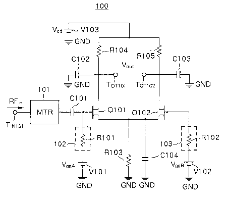
A radio-frequency power detection circuit 100
according to the first embodiment comprises first and
second field-effect transistors (hereinafter, referred to
as a transistor) Q101 and Q102 as two active elements,
capacitors C101, C102, C103 and C104, resistor elements
8101, 8102, 8103 8104 and 8105, voltage sources V101,
VI02 and V103, and a matching circuit (MTR) I01.
A gate of the transistor QI01 is connected to one
electrode of a DC cut capacitor C101, and the other
electrode of the capacitor C101 is connected to an input
terminal TIN101 for a radio-frequency signal RFin via the
matching circuit 101.
Also, a gate of the transistor Q101 is connected to
an end of the resistor element 8101, and the other end of
the resistor element 8101 is connected to the voltage
source VI01 having a voltage of VggA. The resistor
element 8101 configures a first gate bias supply circuit
102 for supplying a gate bias voltage of the transistor
Q101.
A gate of the transistor Q102 is connected to one
CA 02465128 2004-04-28
29
end of the resistor element~102, and the other end of the
resistor element is connected to the voltage source V102
having a voltage of VggB. The resistor element 8102
configures a second gate bias supply circuit 103 for
supplying a gate bias voltage of the transistor Q102.
A source of the transistor Q101 and a source of the
transistor Q102 are connected, and the connection point
is connected to the ground potential GND via the resistor
element 8103 as a current source. Furthermore, between
the connection point of the source of the transistor Q101
and the source of the transistor Q102 and the ground
potential GND, a capacitor (first capacitor) C104 is
connected in parallel with the resistor element 8103.
Note that a capacitance value (capacitance) Css of
the capacitor C104 is set to be a sufficiently large
value, so that between the source terminals of the
transistors Q101 and Q102 and the ground becomes
equivalently short in a radio-frequency signal range. In
other words, the capacitance Css of the capacitor C104 is
set to be a sufficiently large value, so that the
impedance becomes almost 0 ohm (~) in higher frequencies
including an input radio-frequency signal RFin.
A drain of the transistor Q101 is connected to one
end of the resistor element 8104, one electrode of the
capacitor (second capacitor) C102 and a first output
CA 02465128 2004-04-28
terminal TOT101. The other end of the resistor element
8104 is connected to a voltage source V103 having a
voltage of Vdd, and the other electrode of the capacitor
C102 is connected to the ground potential GND.
5 A drain of the transistor Q102 is connected to one
end of the resistor element 8105, one electrode of the
capacitor C103 (third capacitor) and a second output
terminal TOT102. The other end of the resistor element
8105 is connected to the voltage source V103 having a
10 voltage of Vdd, and the other electrode of the capacitor
C103 is connected to the ground potential GND.
The drain of the transistor Q1O1 is supplied with a
drain bias voltage via the resistor element 8104, and the
drain of the transistor Q102 is supplied with a drain
15 bias voltage via the resistor element 8105.
In the radio-frequency power detection circuit 100
configured to have the above connection relationship, the
transistors Q101 and Q102 as active elements have the
same device configuration to have almost the same
20 characteristics.
A gate bias voltage by the gate bias supply circuit
102 and that by the gate bias supply circuit 103 are set
to be approximately the same values. For example, a DC
voltage VggA by the voltage source VI01 and a DC voltage
25 VggB by the voltage source V102 are set to be
CA 02465128 2004-04-28
31
approximately the same~values, and a resistance value of
the resistor element 8101 and that of the resistor
element 8102 are set to be approximately the same values.
Also, a resistance value Rda of the resistor
element 8104 and a resistance value Rda of the resistor
element 8105 connected to the drains of the transistors
Q101 and Q102 satisfy a condition of Rda = Rdb. Similarly,
a capacitance value Couta of the capacitor C102 and a
capacitance value Coutb of the capacitor C103 satisfy a
condition of Couta = Coutb.
Alternatively, in the radio-frequency power
detection circuit 100, when assuming that the ratio
(Wga/Wgb) of a gate width Wga of the transistor Q101 and
the gate width Wgb of the transistor Q102 is N,
conditions of Rda/Rdb = 1/N and Couta = Coutb are
satisfied.
The capacitance values Couta and Coutb of the
capacitors C102 and C103 are set to be sufficiently large
values, so that the impedance becomes almost 0 ohm
in higher frequencies including an input radio-frequency
signal Rfin having a frequency of "fin".
Also, in the gate bias supply circuits 102 and 103,
it is preferable to isolate between gates of the
transistors Q101 and Q102 and a voltage source at an
input signal frequency of "fin"
CA 02465128 2004-04-28
32
Next, an operation in~the above configuration will
be explained.
A radio-frequency signal RFin input to the input
terminal TIN101 is supplied to the gate of the transistor
Q101 via the matching circuit 101 and the DG (direct
current) cut capacitor C101.
Also, the gate of the transistor Q101 is supplied
with a gate bias voltage by the gate bias supply circuit
102 connected to the voltage source V101 for supplying a
voltage of Vgg. Similarly, the gate of the transistor
Q102 is supplied with a gate bias voltage by the gate
bias supply circuit 103 connected to the voltage source
V102 for supplying a voltage of Vgg.
Also, between the connection point of sources of
the transistor Q101 and transistor Q102 and the ground
potential GND, a capacitor C104 is connected in parallel
with the resistor element 8103. Since a capacitance Css
of the capacitor C104 is set to be a sufficiently large
value, so that the impedance becomes almost 0 ohm (~) in
higher frequencies including the input radio-frequency
signal RFin, the sources of the transistors Q101 and Q102
become to be in a stable state in terms of the radio-
frequency.
Also, drains of the transistors Q101 and Q102 are
supplied with drain bias voltages via the resistor
CA 02465128 2004-04-28
33
elements 8104 and R105r respectively.
Since coupling capacitors C102 and C103
respectively having sufficiently large capacitance values
are connected between the drains of the transistors Q101
and Q102 and the ground potential GND, drains of the
transistor Q101 and transistor Q102 become to be in a
stable state in terms of the radio-frequency, and a
voltage difference between a voltage of the drain of the
transistor Q101, that is a voltage of the first output
terminal TOT101, and a voltage of the drain of the
transistor Q102, that is a voltage of the second output
terminal TOT102, is supplied as a detection output signal
to a not shown processing circuit on a subsequent stage.
Below, the detection characteristics of the radio-
frequency power detection circuit in FIG. 7 will be
described with reference to drawings.
FIG. 8 is a view showing an example of detection
characteristics of the radio-frequency power detection
circuit in FIG. 7 and the detection characteristics of a
radio-frequency power detection circuit in FIG. 9
The radio-frequency power detection circuit in FIG.
9 has a circuit configuration wherein a capacitor C104 is
not provided between the connection point of the source
of the transistor Q101 and the source of the transistor
Q102 and the ground potential GND.
CA 02465128 2004-04-28
34
In FIG. 8, an abscissa indicates input radio-
frequency power Pin and an ordinate indicates an output
detection voltage Vout. A frequency of the input radio-
frequency signal is 5.5 GHz. Also, in FIG. 8,
characteristics of the power detection circuit in FIG. 7
is shown by a curve ~, and characteristics of the power
detection circuit in FIG. 9 as comparative data is shown
by a curve ~.
As is known from FIG. 8, the power detection
circuit in FIG. 9 has a better linearity comparing with
that of a conventional power detection circuit, but the
power detection circuit in FIG. 7 has still a better
linearity comparing with that of the power detection
circuit in FIG. 9.
When the input power Pin = -10 dBm, an output
detection voltage Vout = 24 mV in the circuit in FIG. 9,
while in the circuit in FIG. 7, an output detection
voltage Vout = 94 mV is obtained. Namely, the sensitivity
is furthermore improved by about four times as much even
when comparing with that in the circuit in FIG. 9 wherein
sensitivity is improved comparing with the conventional
ci rcui t .
As explained above, according to the present first
embodiment, as a result of configuring that two
transistors (FET) Q101 and Q102 having approximately the
CA 02465128 2004-04-28
same characteristics wherein sources thereof are
connected and the connection point is connected to a
resistor element 8103 as a current source are used as
active elements, gates of the transistors Q101 and Q102
5 are supplied with approximately equal gate bias voltages
by the gate bias supply circuits 102 and 103, drains of
the transistors Q101 and Q102 are supplied with
approximately equal drain bias voltages, between the
connection point of sources of the transistors Q101 and
10 Q102 and the ground potential GND is connected a
capacitor C104 as a first capacitor wherein a capacitance
value is set to be a sufficiently large value so that the
impedance becomes almost 0 ohm in higher frequencies
including an input radio-frequency signal RFin,
15 furthermore, between drains of the transistors Q101 and
Q102 and the ground is connected capacitors C102 and C103
as second and third capacitors wherein capacitance values
are set to be approximately equal and sufficiently large
values so that the impedance becomes almost 0 ohm in
20 higher frequencies including an input radio-frequency
signal Rfin, the gate of the transistor Q101 is supplied
with a radio-frequency signal RFin, and a voltage
difference between the drain of the transistor Q101 and
the drain of the transistor Q102 is regarded as a
25 detection output, effects below are obtained.
CA 02465128 2004-04-28
36
Namely, comparing with a conventional detection
circuit using a silicon Schottky diode, it is suitable to
be made monolithic because it can be configured on a
semiconductor process suitable to a radio-frequency, such
as GaAs. Accordingly, a compact detection circuit
suitable to a radio-frequency operation in a wide band
can be realized at a low cost.
Also, comparing with the conventional power
detection circuit, the power detection circuit in FIG. 7
has an advantage of realizing a high performance radio-
frequency detection circuit having better linearity in
detection characteristics, smaller fluctuation of
detection characteristics against bias fluctuations,
smaller fluctuation of detection characteristics against
FET threshold voltage fluctuation, moreover, a smaller DC
offset.
.Also, since the power detection circuit in FIG. 7
has a balanced output, when the subsequent circuit has a
balanced input, there is an advantage that the connection
becomes easy.
FIG. 10 is a circuit diagram showing a second
embodiment of a radio-frequency power detection circuit
according to the present invention.
A different point in the second embodiment from the
first embodiment explained above is that instead of
CA 02465128 2004-04-28
37
connecting a resistor element as a current source between
the connection point of sources of the transistors Q101
and Q102 and the ground potential GND, a transistor Q103
as a third FET having a gate supplied with a bias
voltage from the third gate bias supply circuit 104, is
connected.
The gate bias supply circuit 104 is configured by a
resistor element 8106 connected between a gate of the
transistor Q104 and the voltage source V104 having a
voltage of VggC.
The other configuration in the second embodiment is
the same as that in the first embodiment.
According to the second embodiment, the same
effects as in the first embodiment can be obtained.
FIG. 11 is a circuit diagram showing a third
embodiment of a radio-frequency power detection circuit
according to the present invention.
The different points in the third embodiment to the
first embodiment explained above are that instead of
connecting the capacitors C102 and C103 between drains of
the transistors Q101 and Q102 and the ground, a capacitor
C105 (second capacitor) wherein the capacitance value is
set to be a sufficiently large value so that the
impedance becomes almost 0 ohm (~) in higher frequencies
including an input radio-frequency signal Rfin is
CA 02465128 2004-04-28
38
connected between a drain of the transistor Q101 and the
drain of the transistor Q102.
The other configuration in the third embodiment is
the same as that in the first embodiment.
According to the third embodiment, the same effects
as in the first embodiment explained above are obtained,
moreover, there are advantages that the number of parts
can be reduced, and the fluctuation (variation) of drain
potentials of the transistors Q101 and Q102 can be
equalized.
FIG. 12 is a circuit diagram showing a fourth
embodiment of the radio-frequency power detection circuit
according to the present invention.
A different point in the fourth embodiment from the
second embodiment explained above is that instead of
connecting the capacitors C102 and C103 between drains of
the transistors Q101 and Q102 and the ground, a capacitor
C106 (second capacitor), wherein the capacitance value is
set to be a sufficiently large value so that the
impedance becomes almost 0 ohm (S2) in higher frequencies
including an input radio-frequency signal Rfin, is
connected between a drain of the transistor Q101 and the
drain of the transistor Q102.
Other configuration in the fourth embodiment is the
same as that in the second embodiment.
CA 02465128 2004-04-28
39
According to the fourth embodiment, the same
effects as in the first embodiment explained above are
obtained, moreover, there are advantages that the number
of parts can be reduced, and the fluctuation of drain
potentials of the transistors Q101 and Q102 can be
equalized.
FIG. 13 is a circuit diagram showing a fifth
embodiment of the radio-frequency power detection circuit
according to the present invention.
A different point in the fifth embodiment from the
first embodiment explained above is that the input form
is not an unbalanced input but a balanced input.
Therefore, in a radio-frequency power detection
circuit 100D according to the fifth embodiment, two input
terminals TIN101 and TIN102 are connected on the input
side of the matching circuit lOla, and two DC cut
capacitors C101a and C101b are connected on the output
side.
A gate of the transistor Q101 is supplied with a
radio-frequency signal RFinA via the DC cut capacitor
C101a, and a gate of the transistor Q102 is supplied with
a radio-frequency signal RFinB via the DC cut capacitor
C101b.
In the radio-frequency power detection circuit 100D
according to the fifth embodiment, a differential power
CA 02465128 2004-04-28
of the radio-frequency signal input RFinA and the radio-
frequency signal input RFinB is detected and output.
The other configuration in the fifth embodiment is
the same as that in the first embodiment.
5 According to the fifth embodiment, the same effects
as in the first embodiment explained above are obtained.
FIG. 14 is a circuit diagram showing a sixth
embodiment of the radio-frequency power detection circuit
according to the present invention.
10 A different point in the sixth embodiment from the
second embodiment explained above is that the input form
is not an unbalanced input but a balanced input.
Therefore, in a radio-frequency power detection
circuit 100E according to the sixth embodiment, two input
15 terminals TIN101 and TIN102 are connected on the input
side of the matching circuit lOlb, and two DC cut
capacitors C101c and C101d are connected on the output
side.
A gate of the transistor Q101 is supplied with a
20 radio-frequency signal RFinA via the DC cut capacitor
C101c, and a gate of the transistor Q102 is supplied with
a radio-frequency signal RFinB via the DC cut capacitor
C101d.
In the radio-frequency power detection circuit 100E
25 according to the sixth embodiment, a differential power
CA 02465128 2004-04-28
41
of the radio-frequencyTsignal input RFinA and the radio-
frequency signal input RFinB is detected and output.
The other configuration in the sixth embodiment is
the same as that in the second embodiment.
According to the sixth embodiment, the same effects
as in the first embodiment explained above are obtained.
FIG. 15 is a circuit diagram showing a seventh
embodiment of the radio-frequency power detection circuit
according to the present invention.
A different point in the seventh embodiment from
the third embodiment explained above is that the input
form is not an unbalanced input but a balanced input.
Therefore, in a radio-frequency power detection
circuit 100F according to the seventh embodiment, two
input terminals TIN101 and TIN102 are connected on the
input side of the matching circuit lOlb, and two DC cut
capacitors C101e and C101f are connected on the output
side.
A gate of the transistor Q101 is supplied with a
radio-frequency signal RFinA via the DC cut capacitor
C101e, and a gate of the transistor Q102 is supplied with
a radio-frequency signal RFinB via the DC cut capacitor
C101f .
In the radio-frequency power detection circuit 100F
according to the seventh embodiment, a differential power
CA 02465128 2004-04-28
42
of the radio-frequency~signal input RFinA and the radio-
frequency signal input RFinB is detected and output.
The other configuration in the seventh embodiment
is the same as that in the third embodiment.
According to the seventh embodiment, the same
effects as in the first embodiment explained above can be
obtained.
FIG. 16 is a circuit diagram showing an eighth
embodiment of the radio-frequency power detection circuit
according to the present invention.
A different point in the eighth embodiment from the
fourth embodiment explained above is that the input form
is not an unbalanced input but a balanced input.
Therefore, in a radio-frequency power detection
circuit 1006 according to the eighth embodiment, two
input terminals TIN101 and TIN102 are connected on the
input side of the matching circuit lOld, and two DC cut
capacitors C101g and C101h are connected on the output
side.
A gate of the transistor Q101 is supplied with a
radio-frequency signal RFinA via the DC cut capacitor
C101g, and a gate of the transistor Q102 is supplied with
a radio-frequency signal RFinB via the DC cut capacitor
C101h.
In the radio-frequency power detection circuit 1006
CA 02465128 2004-04-28
43
according to the eighth embodiment, a differential power
of the radio-frequency signal input RFinA and the radio-
frequency signal input RFinB is detected and output.
The other configuration in the eighth embodiment is
the same as that in the fourth embodiment.
According to the eighth embodiment, the same
effects as in the first embodiment explained above are
obtained.
A variety of embodiments of the radio-frequency
power detection circuit according to the present
invention were explained as the first to eighth
embodiments above.
Below, an N-port demodulator capable of applying
the radio-frequency power detection circuit according to
the present invention will be explained. Note that
instead of eight reference numbers 100, 100A to 1006 used
in the above explanation, a radio-frequency power
detection circuit (PD) is referred to by a reference
number 100H indicating to include any one of the circuits.
FIG. 17 is a circuit diagram showing a
configuration example of a 3-port demodulator capable of
applying a radio-frequency power detection circuit
according to the present invention.
The 3-port demodulator 200 is configured by using
one radio-frequency power detection circuit 100H, and
CA 02465128 2004-04-28
44
further comprises a first signal input terminal TIN201
for a reception signal, a second signal input terminal
TIN202 for a local signal, branch circuits 201 and 202,
phase shifters 203 and 204, a switching circuit 205, and
an N-port signal - IQ signal conversion circuit 206.
Here, the 3-port indicates three ports, that is,
two ports of the first signal input terminal TIN201 for
a reception signal and the second signal input terminal
TIN202 for a local signal added with one port of an
output terminal of the branch circuit 201 to the power
detection circuit 100H.
Note that in the demodulator in FIG. 17, the branch
circuits 201 and 202, phase shifters 203 and 204 and a
switching circuit 205 compose a generation means.
In the 3-port demodulator 200, a reception signal
RS input to the input terminal TIN201 is input to the
branch circuit 201 and branched to two signals. One of
the branched signals is input to the power detection
circuit 100H.
Also, a local signal LS input to the input terminal
TIN202 is input to the branch circuit 202 and branched to
two signals. One of the branched signals is input to the
phase shifter 203 and given a phase shift of 8, then,
input to the switching circuit 205. The other branched
signal is input to the phase shifter 204 and given a
CA 02465128 2004-04-28
phase shift of an angle 8, then, input to the switching
circuit 205. The signals given a phase shift effect by
the phase shifter 203 and the phase shifter 204 are
selectively switched by the switching circuit 205 in
5 order and supplied to the branch circuit 201.
The signal input to the branch circuit 201 is
branched to a signal to be input to the power detection
circuit 100H and two signals to be supplied to the input
terminal TIN201.
10 In the power detection circuit 100H, amplitude
components of the input signal are detected and supplied
to the conversion circuit 206. Then, in the conversion
circuit 206, the input signals are converted to an in-
phase signal (I) and a quadrature signal (Q) as
15 demodulation signals and output.
According to the present 3-port demodulator 200,
since the power detection circuit 100H easily becomes
wide-banded, it can be applied to a system required to
have multi-band or wide band characteristics and respond
20 to demands for radio-frequencies.
Also, since the power detection circuit 100H
operates in a linear range, demodulation is possible even
with a low local signal power and low-skew demodulation
is possible.
25 FIG. 18 is a circuit diagram showing a
CA 02465128 2004-04-28
46
configuration example of time-sharing 4-port demodulator
capable of applying a radio-frequency power detection
circuit according to the present invention.
The 4-port demodulator 300 is configured by using
two radio-frequency power detection circuits 100H-1 and
100H-2, and further comprises a reception signal input
terminal IN301, a local signal input terminal TIN302,
switching circuits 301 and 302, branch circuits 303 and
304, phase shifter 305 and an N-port signal - IQ signal
conversion circuit 306.
Here, the 4-port means four ports, that is, two
ports of the first input terminal TIN301 for a reception
signal and a second input terminal TIN302 for a local
signal added with two ports of an output terminal of the
branch circuit 303 to the power detection circuit 100H-1
and an output terminal of the branch circuit 304 to the
power detection circuit 100H-2.
Note that in the demodulator in FIG. 18, a
generation means is configured by the switching circuits
301 and 302, branch circuits 303 and 304 and a phase
shifter 305.
In the 4-port demodulator 300, the reception signal
RS input to the input terminal TIN301 is input to the
branch circuit 303 via the high speed switching circuit
301 and branched to two signals. One of the branched
CA 02465128 2004-04-28
47
signals is input to the power detection circuit 100H-1
and the other signal is input to the phase shifter 305.
In the phase shifter 305, phase shift 8 is given to
the reception signal from the branch circuit 303, and the
signal given with the phase shift effect is input to the
branch circuit 304 and branched to two signals. In the
branch circuit 304, one of the branched signals is input
to the power detection circuit 100H-2 and the other
signal is supplied to the high speed switching circuit
302 .
Also, the local signal LS input to the input
terminal TIN302 is input to the branch circuit 304 via
the high speed switching circuit 302 and branched to two
signals. One of the branched signals is input to the
power detection circuit 100H-2 and the other signal is
input to the phase shifter 305.
In the phase shifter 305, phase shift 8 is given to
the local signal from the branch circuit 304, and the
signal given with the phase shift effect is input to the
branch circuit 303 and branched to two signals. In the
branch circuit 303, one of the branched signals is input
to the power detection circuit 100H-1, and the other
signal is supplied to the high speed switching circuit
301.
The power detection circuit 100H-1 is supplied with
CA 02465128 2004-04-28
48
a reception signal and~a local signal given with a phase
shift A. In the power detection circuit 100H-1, amplitude
components of the supplied signals are detected and
supplied to the conversion circuit 306.
Also, the power detection circuit 100H-2 is
supplied with a local signal and a reception signal given
with phase shift A. In the power detection circuit 100H-2,
amplitude components of the supplied signals are detected
and supplied to the conversion circuit 306,
In the conversion circuit 306, the input signal is
converted to an inphase signal (I) and a quadrature
signal (Q) and output.
According to the 4-port demodulator, the same
effects as in the 3-port demodulator explained above can
be obtained.
FIG. 19 is a circuit diagram showing a
configuration example of a 5-port demodulator capable of
applying the radio-frequency power detection circuit of
the present invention.
The 5-port demodulator 400 is configured by three
radio-frequency power detection circuits 100H-1, 100H-2
and 100H-3, and furthermore comprises a first signal
input terminal TIN401 for a reception signal, a second
signal input terminal TIN402 for a local signal, a
coupler 401, branch circuits 402 and 403, a phase shifter
CA 02465128 2004-04-28
49
404 and an N-port signal - iQ signal conversion circuit
405.
Here, the 5-port means five ports, that is, two
ports of the reception signal input terminal TIN401, the
local signal input terminal TIN402 added with three ports
of an output terminal of the coupler 401 to the power
detection circuit IOOH-1, an output terminal of the
branch circuit 402 to the power detection circuit 100H-2,
and an output terminal of the branch circuit 403 to the
power detection circuit 100H-3.
Note that in the demodulator in FIG. 19, a
generation means is configured by the coupler 401, the
branch circuits 402 and 403 and the phase shifter 404.
In the 5-port demodulator 400, a reception signal
RS input to the input terminal TIN401 is input to the
branch circuit 402 by the coupler 401, and a part thereof
is input to the power detection circuit 100H-1.
The reception signal input to the branch circuit
402 is branched to two signals. One of the branched
signals is input to the power detection circuit 100H-2,
and the other signal is input to the phase shifter 404.
In the phase shifter 404, phase shift 8 is given to
the reception signal from the branch circuit 402, the
signal given with the phase shift effect is input to the
branch circuit 403 and branched to two signals. In the
CA 02465128 2004-04-28
branch circuit 403, one of the branched signals is input
to the power detection circuit 100H-3 and the other
signal is supplied to the input terminal TIN402.
Also, the local signal LS input to the input
5 terminal TIN402 is input to the branch circuit 403 and
branched to two signals. One of the branched signals is
input to the power detection circuit 100H-3 and the other
signal is input to the phase shifter 404.
In the phase shifter 404, phase shift B is given to
10 the local signal from the branch circuit 403, and the
signal given with the phase shift effect is input to the
branch circuit 402 and branched to two signals. In the
branch circuit 402, one of the branched signals is input
to the power detection circuit 100H-2 and the other
15 signal is supplied to the coupler 401.
The power detection circuit 100H-1 is supplied with
a reception signal. In the power detection circuit 100H-1,
amplitude components of the supplied signal are detected
and supplied to the conversion circuit 405.
20 The power detection circuit 100H-2 is supplied with
a reception signal and a local signal given with phase
shift 8. In the power detection circuit 100H-2, amplitude
components of the supplied signal are detected and
supplied to the conversion circuit 405.
25 Also, the power detection circuit 100H-3 is
CA 02465128 2004-04-28
51
supplied with a local Signal and a reception signal given
with phase shift 8. In the power detection circuit 100H-3,
amplitude components of the supplied signal are detected
and supplied to the conversion circuit 405.
In the conversion circuit 405, the input signal is
converted to an inphase signal (I) and a quadrature
signal (Q) and output.
According to the 5-port demodulator, the same
effects as in the 3-port demodulator explained above can
be obtained.
FIG. 20 is a circuit diagram of a configuration
example of 6-port demodulator capable of applying the
radio-frequency power detection circuit according to the
present invention.
The 6-port demodulator 500 is configured by four
power detection circuits 100H-1, 100H-2, 100H-3 and 100H-
4, and furthermore comprises a first signal input
terminal TIN50I for a reception signal, a second signal
input terminal TIN502 for a local signal, couplers 501
and 502, branch circuits 503 and 504, a phase shifter 505
and an N-port signal - IQ signal conversion circuit 506.
Here, the 6-port means six ports, that is, two
ports of the reception signal input terminal TIN50I and
the local signal input terminal TIN502, added with four
ports of an output terminal of the coupler 401 to the
CA 02465128 2004-04-28
52
power detection circuit 100H-1, an output terminal of the
branch circuit 402 to the power detection circuit 100H-2,
an output terminal of the branch circuit 403 to the power
detection circuit 100H-3, and an output terminal of the
coupler 402 to the power detection circuit 100H-4.
Note that in the demodulator in FIG. 20, a
generation means is configured by the couplers 501 and
502, branch circuits 503 and 504, and a phase shifter 505.
In the 6-port demodulator 500, a reception signal
RS input to the input terminal TIN501 is input to the
branch circuit 503 by the coupler 501, and a part thereof
is input to the power detection circuit 100H-1,
The reception signal input to the branch circuit
503 is branched to two signals. One of the branched
signals is input to the power detection circuit 100H-2
and the other signal is input to the phase shifter 505.
In the phase shifter 505, phase shift 6 is given to
the reception signal from the branch circuit 503, the
signal given with the phase shift effect is input to the
branch circuit 504 and branched to two signals. In the
branch circuit 504, one of the branched signals is input
to the power detection circuit 100H-3 and the other
signal is input to the coupler 502.
In the coupler 502, the input signal is supplied to
the input terminal TIN502 by the coupler 501.
CA 02465128 2004-04-28
53
Also, a local signal LS input to the input terminal
TIN502 is input to the branch circuit 504 by the coupler
502, and a part thereof is input to the power detection
circuit 100H-4.
The local signal input to the branch circuit 504 is
branched to two signals. One of the branched signals is
input to the power detection circuit 100H-3 and the other
signal is input to the phase shifter 504.
In the phase shifter 504, phase shift A is given to
the local signal from the branch circuit 504, and the
signal given with the phase shift effect is input to the
branch circuit 503 and branched to two signals. In the
branch circuit 503, one of the branched signals is input
to the power detection circuit 100H-2 and the other
signal is supplied to the coupler 501.
The power detection circuit 100H-1 is supplied only
with the reception signal. In the power detection circuit
100H-1, amplitude components of the supplied reception
signal are detected and supplied to the conversion
circuit 506.
The power detection circuit 100H-2 is supplied with
a reception signal and a local signal given with phase
shift 8. In the power detection circuit 100H-2, amplitude
components of the supplied signal are detected and
supplied to the conversion circuit 506.
CA 02465128 2004-04-28
54
Also, the power detection circuit 100H-3 is
supplied with a local signal and a reception signal given
with phase shift A. In the power detection circuit 100H-3,
amplitude components of the supplied signal are detected
and supplied to the conversion circuit 506.
Also, the power detection circuit 100H-4 is
supplied only with a local signal. In the power detection
circuit 100H-4, amplitude components of the supplied
signal are detected and supplied to the conversion
circuit 506.
In the conversion circuit 505, the input signal is
converted to an inphase signal (I) and a quadrature
signal (Q) as demodulation signals and output.
According to the 6-port demodulator, the same
effects as in the 3-port demodulator explained above can
be obtained.
FIG. 21 is a circuit diagram showing another
configuration example of 3-port demodulator capable of
applying the radio-frequency power detection circuit
according to the present invention.
A different point in the 3-port demodulator 200A in
FIG. 21 from the demodulator 200 in FIG. 17 is that drain
bias voltages of transistors Q101 and Q102 of a power
detection circuit 100I are changed in accordance with
reception signal level information, specifically, it is
CA 02465128 2004-04-28
controlled by a control circuit 207 to set the drain bias
voltages low when the reception signal level is lower
than a predetermined level.
Note that the power detection circuit 1001 is a
5 power detection circuit (PD) indicated by the reference
number 100I indicating to include any one of the circuits
instead of the eight reference numbers 100 and 100A to
1006 according to the first to eight embodiments
explained above. Note that the power detection circuit
10 100I is a circuit equivalent to a circuit (not including
the voltage source V103), wherein the voltage source V103
composing the drain bias supply circuit in the eight
circuits 100 and 100A to 1006 according to the first to
eight embodiments is taken out as a circuit 208.
15 A conversion circuit 206A of the 3-port demodulator
200A in FIG. 21 has a function as a level detection
circuit for detecting a reception signal level and
supplying the same as a reception signal level signal
S206 to a control circuit 207 in addition to a function
20 of converting an input signal to an inphase signal (I)
and a quadrature signal (Q) as demodulation signals based
on amplitude components of the input signal detected in
the power detection circuit 100I.
As explained above, the drain bias supply circuit
25 208 taken out from the power detection circuit 100I has,
CA 02465128 2004-04-28
56
for example, on the output .side of the voltage source
V103 of 3V a DC-DC converter 208A for changing a drain
bias voltage Vd in accordance with a control signal CTL
of the control circuit 207. An output voltage of the DC-
DC converter 208A is supplied to drains of the
transistors Q101 and Q102 via resistor elements 8104 and
8105 in the eight circuits 100 to 100A to 1006 according
to the first to eight embodiments.
The control circuit 207 receives a reception signal
level signal 5206 from the conversion circuit 206A and
outputs a control signal CTL to the DC-DC converter 208A
to supply the drain bias voltage Vd in accordance with
the reception signal level.
Specifically, when the reception signal level
(power) is -10 dBm to -5 dBm, the control circuit 207
generates a control signal CTL to supply as it is as 3V,
when the reception signal level (power) is -25 dBm to -15
dBm, generates a control signal CTL to lower to 2V to
supply, when the reception signal level (power) is -100
dBm to -25 dBm, generates a control signal CTL to lower
to 1V to supply and outputs to the DC-DC converter.
Namely, the control circuit 207 generates a control
signal CTL to lower the supply voltage of the voltage
source 103 by 30~ to 70~ in accordance with the reception
signal level.
CA 02465128 2004-04-28
57
FIG. 22 is a view showing input power dependency of
an output detection voltage of the radio-frequency power
detection circuit when changing the drain bias voltage in
accordance with reception signal level information.
In FIG. 22, an abscissa indicates input radio-
frequency power Pin and an ordinate indicates an output
detection voltage Vout. A frequency of the input radio-
frequency signal is 5.5 GHz. In FIG. 22, characteristics
of the power detection circuit when the drain bias
voltage Vd is 3V is shown by a curve (1), characteristics
of the power detection circuit when the drain bias
voltage Vd is 2V is shown by a curve (2), and
characteristics of the power detection circuit when the
drain bias voltage Vd is 1V is shown by a curve (3).
As is known from FIG. 22, when the reception signal
level is low, linearity is maintained even when the drain
bias voltage is lowered.
Accordingly, according to the demodulator 200A in
FIG. 21, the power detection circuit 100I easily becomes
wide-banded, so that it can be applied to a system
required to have multi-band or wide-band characteristics,
respond to demands for higher frequencies. Furthermore,
since the power detection circuit 100I operates in a
linear range, there are advantages that demodulation with
low local signal power is possible, low-skew demodulation
CA 02465128 2004-04-28
58
is possible, and power~saving is attained when the
reception signal level is low.
FIG. 23 is a circuit diagram showing another
configuration example of a 4-port demodulator capable of
applying the radio-frequency power detection circuit
according to the present invention.
A different point in a 4-port demodulator 300A in
FIG. 23 from the demodulator 300 in FIG. 18 is that drain
bias voltages of the transistors Q101 and Q102 of the
power detection circuits 100I-1 and 100I-2 are changed in
accordance with reception signal level information,
specifically, it is controlled by a control circuit 307
to set the drain bias voltages low when the reception
signal level is lower than a predetermined level.
Note that the power detection circuits 100I-1 and
100I-2 indicate a radio-frequency power detection circuit
(PD) indicated by the reference number 100I indicating to
include any one of the circuits instead of the eight
reference numbers 100 and 100A to 1006 according to the
first to eight embodiments explained above. Note that the
power detection circuit 100I is a circuit equivalent to a
circuit (not including the voltage source V103), wherein
the voltage source V103 composing the drain bias supply
circuit in the eight circuits 100 and 100A to 1006
according to the first to eight embodiments is taken out
CA 02465128 2004-04-28
59
as a circuit 308. The drain bias circuit 308 is shared by
the power detection circuits 100I-1 and 100I-2.
A conversion circuit 306A of the 4-port demodulator
300A in FIG. 23 has a function as a level detection
circuit for detecting a reception signal level and
supplying the same as a reception signal level signal
S306 to a control circuit 307 in addition to a function
of converting an input signal to an inphase signal (I)
and a quadrature signal (Q) as demodulation signals based
on amplitude components of the input signal detected in
the power detection circuits 100I-1 and 100I-2.
As explained above, the drain bias supply circuit
308 taken out from the power detection circuits 100I-1
and 100I-2 to be shared has, for example, on the output
side of the voltage source V103 of 3V a DC-DC converter
308A for changing a drain bias voltage Vd in accordance
with a control signal CTL of the control circuit 307. An
output voltage of the DC-DC converter 308A is supplied to
drains of the transistors Q101 and Q102 via resistor
elements 8104 and 8105 in the eight circuits 100 to 100A
to 1006 according to the first to eight embodiments.
The control circuit 307 receives a reception signal
level signal S306 from the conversion circuit 306A and
outputs a control signal CTL to the DC-DC converter 308A
to supply the drain bias voltage Vd in accordance with
CA 02465128 2004-04-28
the reception signal level.
Specifically, when the reception signal level
(power) is -10 dBm to -5 dBm, the control circuit 307
generates a control signal CTL to supply as it is as 3V,
5 when the reception signal level (power) is -25 d8m to -I5
dBm, generates a control signal CTL to lower to 2V to
supply, when the reception signal level (power) is -100
d8m to -25 dBm, generates a control signal CTL to lower
to 1V to supply and outputs to the DC-DC converter.
10 Namely, the control circuit 307 generates a control
signal CTL to lower the supply voltage of the voltage
source 103 by 30~ to 70~ in accordance with the reception
signal level.
Input power dependency of an output detection
15 voltage of the radio-frequency power detection circuits
100H-1 and 100I-2 applied to the demodulator 300A in FIG.
23 can obtain the same characteristic as that in FIG. 22.
Namely, the radio-frequency power detection
circuits 100I-1 and 100I-2 maintain linearity even when
20 the reception signal level is low or the drain bias
voltage is lowered.
Accordingly, according to the demodulator 300A in
FIG. 23, the power detection circuits 100I-1 and 100I-2
easily become wide-banded, so that they can be applied to
25 a system required to have multi-band or wide-band
CA 02465128 2004-04-28
61
characteristics, respond to~demands for higher
frequencies. Furthermore, since the power detection
circuits 100I-1 and 100I-2 operate in a linear range,
there are advantages that demodulation with low local
signal power is possible, low-skew demodulation is
possible, and power saving is attained when the reception
signal level is low.
FIG. 24 is a circuit diagram showing another
configuration example of a 5-port demodulator capable of
applying the radio-frequency power detection circuit
according to the present invention.
A different point in a 5-port demodulator 400A in
FIG. 24 from the demodulator 400 in FIG. 19 is that drain
bias voltages of the transistors Q101 and QI02 of the
power detection circuits 100I-1, 100I-2 and 100I-3 axe
changed in accordance with reception signal level
information, specifically, it is controlled by a control
circuit 406 to set the drain bias voltages low when the
reception signal level is lower than a predetermined
level .
Note that the power detection circuits 100I-1 to
100I-3 indicate a radio-frequency power detection circuit
(PD) indicated by the reference number 100I indicating to
include any one of the circuits instead of the eight
reference numbers 100 and 100A to 1006 according to the
CA 02465128 2004-04-28
62
first to eight embodiments explained above. Note that the
power detection circuit 100I is a circuit equivalent to a
circuit (not including the voltage source V103), wherein
the voltage source V103 composing the drain bias supply
circuit in the eight circuits 100 and 100A to 1006
according to the first to eight embodiments is taken out
as a circuit 407. The drain bias supply circuit 407 is
shared by the power detection circuits 100I-1 and 100I-2.
A conversion circuit 405A of the 5-port demodulator
400A in FIG. 24 has a function as a level detection
circuit for detecting a reception signal level and
supplying the same as a reception signal level signal
5405 to a control circuit 406 in addition to a function
of converting an input signal to an inphase signal (I)
and a quadrature signal (Q) as demodulation signals based
on amplitude components of the input signal detected in
the power detection circuits 100I-1 to 100I-3.
As explained above, the drain bias supply circuit
407 taken out from the power detection circuits 100I-1 to
100I-3 to be shared has, for example, on the output side
of the voltage source V103 of 3V a DC-DC converter 407A
for changing a drain bias voltage Vd in accordance with a
control signal CTL of the control circuit 406. An output
voltage of the DC-DC converter 407A is supplied to drains
of the transistors Q101 and Q102 via resistor elements
CA 02465128 2004-04-28
63
8104 and 8105 in the eight circuits 100 to 100A to 1006
according to the first to eight embodiments.
The control circuit 406 receives a reception signal
level signal 5405 from the conversion circuit 405A and
outputs a control signal CTL to the DC-DC converter 407A
to supply the drain bias voltage Vd in accordance with
the reception signal level.
Specifically, when the reception signal level
(power) is -10 dBm to -5 dBm, the control circuit 406
generates a control signal CTL to supply as it is as 3V,
when the reception signal level (power) is -25 dBm to -15
dBm, generates a control signal CTL to lower to 2V to
supply, when the reception signal level (power) is -100
dBm to -25 dBm, generates a control signal CTL to lower
to 1V to supply and outputs to the DC-DC converter.
Namely, the control circuit 406 generates a control
signal CTL to lower the supply voltage of the voltage
source 103 by 30$ to 705 in accordance with the reception
signal level.
Input power dependency of an output detection
voltage of the radio-frequency power detection circuits
100H-1 to 100I-3 applied to the demodulator 400A in FIG.
24 can obtain the same characteristic as that in FIG. 22.
Namely, the radio-frequency power detection
circuits 100I-1 to 100I-3 maintain linearity even when
CA 02465128 2004-04-28
64
the reception signal level is low or the drain bias
voltage is lowered.
Accordingly, according to the demodulator 400A in
FIG. 24, the power detection circuits 100I-1 to 100I-3
easily become wide-banded, so that they can be applied to
a system required to have multi-band or wide-band
characteristics, respond to demands for higher
frequencies. Furthermore, since the power detection
circuits 100I-1 to 100I-3 operate in a linear range,
there are advantages that demodulation with low local
signal power is possible, low-skew demodulation is
possible, and power saving is attained when the reception
signal level is low.
FIG. 25 is a circuit diagram showing another
configuration example of a 6-port demodulator capable of
applying the radio-frequency power detection circuit
according to the present invention.
A different point in a 6-port demodulator 500A in
FIG. 25 from the demodulator 500 in FIG. 20 is that drain
bias voltages of the transistors Q101 and Q102 of the
power detection circuits 100I-1, 100I-2, 100I-3 and 100I-
4 are changed in accordance with reception signal level
information, specifically, it is controlled by a control
circuit 507 to set the drain bias voltages low when the
reception signal level is lower than a predetermined
CA 02465128 2004-04-28
level.
Note that the power detection circuits 100I-1 to
100I-4 indicate a radio-frequency power detection circuit
(PD) indicated by the reference number IOOI indicating to
5 include any one of the circuits instead of the eight
reference numbers 100 and 100A to 1006 according to the
first to eight embodiments explained above. Note that the
power detection circuit 100I is a circuit equivalent to a
circuit (not including the voltage source V103), wherein
10 the voltage source V103 composing the drain bias supply
circuit in the eight circuits 100 and 100A to 1006
according to the first to eight embodiments is taken out
as a circuit 508. The drain bias circuit 508 is shared by
the power detection circuits 100I-1 to IOOI-4.
15 A conversion circuit 506A of the 5-port demodulator
500A in FIG. 25 has a function as a level detection
circuit for detecting a reception signal level and
supplying the same as a reception signal level signal
5506 to a control circuit 507 in addition to a function
20 of converting an input signal to an inphase signal (I)
and a quadrature signal (Q) as demodulation signals based
on amplitude components of the input signal detected in
the power detection circuits 100I-1 to 100I-4.
As explained above, the drain bias supply circuit
25 508 taken out from the power detection circuits 100I-1 to
CA 02465128 2004-04-28
66
100I-4 to be shared has, fox example, on the output side
of the voltage source V103 of 3V a DC-DC converter 508A
for changing a drain bias voltage Vd in accordance with a
control signal CTL of the control circuit 507. An output
voltage of the DC-DC converter 508A is supplied to drains
of the transistors Q101 and Q102 via resistor elements
8104 and 8105 in the eight circuits 100 to 100A to 1006
according to the first to eight embodiments.
The control circuit 507 receives a reception signal
level signal 5506 from the conversion circuit 506A and
outputs a control signal CTL to the DC-DC converter 508A
to supply the drain bias voltage Vd in accordance with
the reception signal level.
Specifically, when the reception signal level
(power) is -10 dBm to -5 dBm, the control circuit 507
generates a control signal CTL to supply as it is as 3V,
when the reception signal level (power) is -25 dBm to -15
dBm, generates a control signal CTL to lower to 2V to
supply, when the reception signal level (power) is -100
dBm to -25 dBm, generates a control signal CTL to lower
to 1V to supply and outputs to the DC-DC converter.
Namely, the control circuit 507 generates a control
signal CTL to lower the supply voltage of the voltage
source 103 by 30~ to 70~ in accordance with the reception
signal level.
CA 02465128 2004-04-28
67
The input power dependency of an output detection
voltage of the radio-frequency power detection circuits
100H-1 to 100I-4 applied to the demodulator 500A in FIG.
25 can obtain the same characteristic as that in FIG. 22.
Namely, the radio-frequency power detection
circuits 100I-1 to 100I-4 maintain linearity even when
the reception signal level is low or the drain bias
voltage is lowered.
Accordingly, according to the demodulator 500A in
FIG. 25, the power detection circuits 100I-1 to 100I-4
easily become wide-banded, so that they can be applied to
a system required to have multi-band or wide-band
characteristics, respond to demands for higher
frequencies. Furthermore, since the power detection
circuits 100I-1 to 100I-4 operate in a linear range,
there are advantages that demodulation with low local
signal power is possible, low-skew demodulation is
possible, and power saving is attained when the reception
signal level is low.
Industrial Applicability
As explained above, according to a power detection
circuit according to the present invention and a
demodulator using the same, comparing with a detection
circuit using a silicon Schottky diode, since it can be
CA 02465128 2004-04-28
68
configured on a semiconductor process suitable to radio-
frequencies, such as GaAs, it is suitable to be made
monolithic. Accordingly, a compact detection circuit
being wide-banded and suitable to a radio-frequency
operation can be realized at low costs. Also, the power
detection circuit of the present invention can realize a
high performance radio-frequency power detection circuit
having excellent linearity in detection characteristics,
small fluctuation in detection characteristics against
bias fluctuation, small fluctuation in detection
characteristics against FET threshold voltage fluctuation,
and small DC offset. Also, the power detection circuit of
the present invention has a balanced output, so that when
a subsequent circuit has a balanced input, the connection
becomes easy.
CA 02465128 2004-04-28
Explanation of References
100, 100A to 1006. . . radio-frequency power detection circuit
101, lOla to lOld...matching circuit
102, 102a...first gate bias supply circuit
103, 103a...second gate bias supply circuit
104, 104a...third gate bias supply circuit
Q101, Q101a...first field-effect transistor
Q102, Q102a...second field-effect transistor
Q103...third field-effect transistor
C101 to C106...capacitor
8101 to R107...resistor element
V101 to V103...voltage source
200, 200A...3-port demodulator
100H, 100I...radio-frequency power detection circuit
TIN201...first signal input terminal
TIN202...second signal input terminal
201, 202...branch circuit
203, 204...phase shifter
205...switching circuit
206, 206A...N-port signal - IQ signal conversion circuit
207... control circuit
108...drain bias supply circuit
108A...DC-DC converter
300, 300A...4-port demodulator
100H-1, 100H-2, 100I-1, 100I-2... radio-frequency power
detection circuit
26/28
CA 02465128 2004-04-28
TIN301...first signal input terminal
TIN302...second signal input terminal
301, 302...switching circuit
303, 304...branch circuit
305...phase shifter
306, 306A...N-port signal - IQ signal conversion circuit
307... control circuit
308...drain bias supply circuit
308A...DC-DC converter
400, 400A...5-port demodulator
100H-1 to 100H-3, 100I-1 to 100I-3. . . radio-frequency power
detection circuit
TIN401...first signal input terminal
TIN402...second signal input terminal
401...coupler
402, 403...branch circuit
404...phase shifter
405, 405A...N-port signal - IQ signal conversion circuit
406...control circuit
407...drain bias supply circuit
407A...DC-DC converter
500, 500A...6-port demodulator
100H-1 to 100H-4, 100I-1 to 100I-4... radio-frequency power
detection circuit
TIN501...first signal input terminal
27/28
CA 02465128 2004-04-28
TIN502...second signal input terminal
501, 502...coupler
503, 504...branch circuit
505...phase shifter
506, 506A...N-port signal - IQ signal conversion circuit
507... control circuit
508...drain bias supply circuit
508A...DC-DC converter
28/28