Note: Descriptions are shown in the official language in which they were submitted.
CA 02466064 2004-04-30
WO 03/055077 PCT/US02/34848
ENCODER SELF-CALIBRATION APPARATUS AND METHOD
Cross-Reference Section
This application claims priority of provisional application 60/336,038 filed
November 2, 2001.
Background of the Invention
As encoders have become more and more sophisticated and high precision, their
setup and alignment has become more and more critical. Some encoders are
completely
sealed units and are thusly aligned and calibrated at the factory under ideal
conditions. On
the other hand, many other encoders, such as those sold by the assignee of the
present
invention, are delivered to customers as components or subsystems. There are
several
benefits of to this approach, however it does preclude full factory
setup/alignment.
Therefore, various means have been developed to aid customers during the
installation
and setup of this class of encoder.
Typical early attempts at helping customers set up these encoders comprised
not
much more than providing a set of test points in the electronics and a
systematic written
procedure to follow. More recently, various sensing circuits have been
included in the
encoder electronics that provide some indication of proper alignment and/or
inform the
user about calibration adjustments.
The prior art alignment aids do not provide any automatic calibration
features. At
best they seem to give a general indication of signal strength (i.e., is the
electrical
sinusoid too weak or too strong). For optimal operation, the relative phase
between the
quadrature signals should be as close to 90 degrees as possible, their
relative gains should
be equalized, and their individual offsets should be set to zero. To the
extent possible,
these calibration operations should be transparent to the user (that is, not
require the user
to make fine electrical adjustments).
In addition to these calibrations, modern encoders also have index (or
reference)
marks. The output index pulses should occur every time the scale is in the
same position
relative to the encoder head. Thus another problem addressed by this invention
is the need
-1-
CA 02466064 2004-04-30
WO 03/055077 PCT/US02/34848
to calibrate the index pulse generation system such that the index pulse is
generated at the
same scale location to within an LSB of the encoder measurement.
Summary of the Invention
Circuitry and firmware logic built into the processing unit allow a user to
quickly
setup an encoder by simply running the encoder scale under the head a few
times.
Indicator lights on the connector notify the user of processor and encoder
status.
During the self-calibration cycle the encoder processor can automatically
adjust
itself in terms of amplifier gain and offset and signal quadrature phase
shift. Also, the
disclosed method automatically places the index pulse near the center of the
index
window with a 1 LSB repeatability with respect to the "zero-location" fringe.
Also, the
disclosed apparatus communicates its status to the user with a simple LED
display so all
of these operations are performed without external test or monitoring
equipment.
In one aspect, the invention provides a method of calibrating an optical
encoder of
the type that generates two analog quadrature signals, x, y. The method
includes a step of
generating a plurality of digital samples, x;, y;, of the analog signals x, y,
i having integer
values from one to an integer n larger than one. The method also includes
generating a
plurality calibrated samples X;, Y;, according to the equation
X; _ ~x; + Ox; + P x y; ~x Gx;
Gx; and Gy; being scaling coefficients, Ox; and Oy; being
Y,. _ ( y; + Oy; ~ x Gy;
offset coefficients, and P; being phase coefficients. The method also includes
generating
a plurality of magnitude M;, and phase, ~;, samples according to the equations
M; = X z+YZ
~; = aTAN ~ ,
M; and ~; defining one sample of a phasor V;, according to the equation
Va = Mr exP~j~r
j being the complex number square root of negative one. The phasor V; may be
represented by a line segment in a two-dimensional coordinate system. The
phasor has a
-2-
CA 02466064 2004-04-30
WO 03/055077 PCT/US02/34848
first end and a second end. The first end lies at the origin of the coordinate
system. The
second end is displaced from the first end by a length equal to the magnitude
M;, in a
direction defined by an angle relative to the x axis equal to the phase ~;.
The method also
includes providing initial values for the scaling coefficients, Gx; and Gyp,
the offset
coefficients, Ox, and Oy~, and the phase coefficients, P;. The method also
includes
adjusting the values of the scaling coefficients, the offset coefficients, and
the phase
coefficients so that
and
Gx;+; equals either Gx; or Gx; plus or minus an incremental adjustment,
Gy;+, equals either Gy; or Gy; plus or minus an incremental adjustment,
Ox;+1 equals either Ox; or Ox; plus or minus an incremental adjustment,
Oy;+; equals either Oy; or Oy; plus or minus an incremental adjustment,
P;+; equals either P; or P; plus or minus an incremental adjustment.
The incremental adjustments to the coefficients are made so as to move the
second
end of the phasor closer to a circle of predetermined radius (such as a unit
circle) centered
about the origin of the coordinate system. More specifically, the incremental
adjustments
to the coefficients may be made so that a distance between the second end of a
hypothetical phasor V'; and the unit circle is less than or equal to a
distance between a
second end of the phasor V; and the circle. The hypothetical phasor V'; is
determined by
the following equations:
X '; _ (x; + Ox;+~ + 1'+~ X Yr ~ X Gx;+~
Ya = ~Y, + OYr+i ~ X GYr+t
= X.2+Y~z
~'; = ATAN X'.
V~; = M~~ exp~j~'~
In one alternative of the method, the coefficients Gx; and Ox;, may be
adjusted
once while V; lies in one half of the circle, and may not be adjusted again
until Vk lies in
the other half of the circle, k being greater than i. In another alternative,
the coefficients
Gx; and Ox;, may be adjusted once while V; lies in the left half of the
circle, and may not
-3-
CA 02466064 2004-04-30
WO 03/055077 PCT/US02/34848
be adjusted again until Vk lies in the right half of the circle, k being
greater than i. In
another alternative, the coefficients Gy; and Oy;, may be adjusted once while
V; lies in
one half of the circle, and may not be adjusted again until Vk lies in the
other half of the
circle, k being greater than i. In another alternative, the coefficients Gy;
and Oy;, may be
adjusted once while V; lies in the upper half of the circle, and may not be
adjusted again
until Vk lies in the lower half of the circle, k being greater than i. In
another alternative,
the coefficient P; may be adjusted once while V; lies in a quadrant of the
circle, and may
not be adjusted again until Vk lies in a different quadrant of the circle, k
being greater
than i. Also, the values of the coefficients may be adjusted according to the
following
table:
Magnitude Magnitude
> unit < unit
circle circle
radius radius
Angle Angle Space Offset Phase Gain Offset Phase
(in (in
degrees)degrees)T
From: o:
348.75 11.25 0 Gx=Gx-1 Ox=Ox-1- Gx=Gx+1 Ox=Ox+1 -
11 33 1
25 75
. .
33.75 56.25 2 - - P=P-1 - - P=P+1
56 78 3
25 75
. .
78.75 101.25 4 Gy=Gy-1 Oy=Oy-1- Gy=Gy+1 Oy=Oy+1 -
101.25 123.75 5
123.75 146.25 6 - - P=P+1 - - P=P-1
146.25 168.75 7
168.75 191.25 8 Gx=Gx-1 Ox=Ox+1- Gx=Gx+1 Ox=Ox-1 -
191.25 213.75 9
213.75 236.25 10 - - P=P-1 - - P=P+1
236.25 258.75 11
258.75 281.25 12 Gy = Oy = - Gy = Oy = -
Gy - Oy Gy + Oy -
1 + 1 1 1
281.25 303.75 13
303.75 326.25 14 - - P=P+1 - - P=P-1
326.25 348.75 15
if Magnitud e = unite radius ts are ed
circl then adjust
no
coefficien
wherein the increment value "1" is one least significant bit.
-4-
CA 02466064 2004-04-30
WO 03/055077 PCT/US02/34848
In another aspect, the invention provides method of processing signals
generated
by an optical encoder. The method includes generating samples of phase, ~;,
according
to the equation
~; = ATAN Y' , where X; and Y; are samples of quadrature signals received
Xa
from the encoder, and where i is an integer having values from one to an
integer n.
The method also includes generating a count. The count increases by one every
time the phase, when measured modulo two pi, crosses from a fourth quadrant of
a unit
circle to a first quadrant of the unit circle. The count decreases by one
every time the
phase, when measured modulo two pi, crosses from the i~irst quadrant of the
unit circle to
the fourth quadrant of the unit circle. The fourth quadrant extends from
angles 3/2 pi to 2
pi. The first quadrant extends from angles zero to pi/2. The method also
includes
generating two burst output signals in A quad B format by: generating an
integer number
representative of the count and the phase ~;; generating a running sum by
counting
transitions in the A quad B burst output signals, using known standard methods
of
counting transitions in A quad B format signals; generating a signed
difference value
representative of a difference between the integer number and the running sum;
and
generating transitions in the A quad B burst output signals until the signed
difference
value is zero.
In this method, the samples of phase ~; may be represented as binary numbers
having Dmax bits, Dmax being a pre-determined integer. The integer number may
be
represented as a binary number having d bits, d being a pre-determined
integer. The
integer number has D least significant bits and d minus D most significant
bits, D being a
user selectable integer that is greater than zero, less than d, and less than
Dmax. The
integer number may be generated by setting the D least significant bits of the
integer
number equal to the D most significant bits of the phase ~;, and by setting
the d minus D
most significant bits of the integer number equal to the d minus D least
significant bits of
the count. Alternatively, D may be the smallest integer satisfying the
equation D >_ Dmax
+ log(S)/log(2), where S is a user selectable scale factor. The method may
include
-5-
CA 02466064 2004-04-30
WO 03/055077 PCT/US02/34848
generating a scaled phase O;, equal to a product of the phase ~; and the user
selectable
scale factor S. The integer number may be generated by setting the D least
significant
bits of the integer number equal to the D least significant bits of the scaled
phase O;, and
by setting the d minus D most significant bits of the integer number equal to
the d minus
D least significant bits of the count.
In another aspect, the invention provides a method of generating an index
signal
for an optical encoder. The encoder generates quasi-sinusoidal quadrature
signals
indicative of a position of a scale relative to a sensor head. The encoder
also generates a
window signal. The window signal is characterized by a high value whenever an
index
mark of the scale is aligned with the sensor head. The window signal being
characterized
by a low value whenever the index mark is not aligned with the sensor head.
The method
includes setting a first number equal to the value of the phase when the
window signal
transitions from a low value to a high value; and setting a second number
equal to the
value of the phase when the window signal transitions from a high value to a
low value.
If a difference between the first number and the second number is greater than
pi and less
than 3 pi, then a phase index may be set equal to value that is between the
first and second
numbers. The method includes generating the index signal whenever the window
signal
is characterized by a high value and when the phase is substantially equal to
the phase
index. The phase index may be set equal to a median value between the first
number and
the second number. The steps of recording the phase values when at transitions
of the
window signal and of setting the phase index may be performed only after
receipt of a
calibration command. An indication to a user may be provided when the window
signal
is characterized by a high value. The indication to the user may be provided
by activating
a light source.
Brief Description of the Figures
Figure 1 shows a block diagram of encoder processing electronics constructed
according to the invention.
Figure 2 shows a block diagram of the phase processor shown in Figure 1.
Figure 3 illustrates calibration adjustments made according to the invention.
-6-
CA 02466064 2004-04-30
WO 03/055077 PCT/US02/34848
Figure 4 illustrates calculation of an index point according to the invention.
Figure 5 shows a block diagram for calculating the index point according to
the
invention.
Figures 6A and 6B show top and side views, respectively, of connectors housing
processing electronics constructed according to the invention.
Figure 7 illustrates A quad B signals and an index pulse.
Figure 8A illustrates motion of a scale in an encoder.
Figures 8B and 8E illustrate sine and cosine signals, respectively, generated
by an
encoder.
Figures 8C and 8F illustrate the A and B, respectively, portions of an A quad
B
signal generated by an encoder.
Figures 8D and 8G illustrate the A and B, respectively, of a burst,A quad B
signal
generated according to the invention.
Figure 9 shows a block diagram of a method for generating the signals shown in
Figures 8D and 8G according to the invention.
Figure 10 illustrates a method according to the invention by which the user
interface logic communicates with the user.
Detailed Description of the Invention
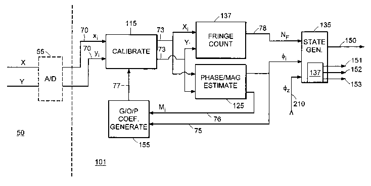
Figure 1 shows an optical encoder system 10 comprising a sensor head 50 that
observes the relative motion of a scale 60 and associated signal processing
electronics
100. As discussed below, the processing electronics 100 automatically
calibrates the
encoder's position measuring circuits and index pulse generating circuits. The
electronics
100 are preferably implemented in a miniaturized form factor that includes
firmware
programmable logic, however, other implementations of the electronics 100 are
embraced
within the invention.
CA 02466064 2004-04-30
WO 03/055077 PCT/US02/34848
The Sensor Head
The sensor head 50 and scale 60 preferably cooperate in a known fashion to
produce two families of signals. One family of signals provide information
about the
displacement of scale relative to the sensor head. These signals are the
quadrature signals
70. The second family of signals is the index window signals 80; these signals
indicate
when a specific location on the scale 60 passes by the sensor head 50.
In one preferred implementation the analog quadrature signals internal to the
sensor head 50 have a generally sinusoidal strength variation that is related
to the
displacement of the scale 60. These "x" and "y" signals are ideally shifted
from one
another by 90 degrees of phase. These analog signals are typically sampled and
converted
to digital values in sensor head 50 by Analog-to-Digital converter 55; the
digital output
values 70 are denoted by "x;" and "y;" respectively in Figure 2, where the
subscripted "i"
indicates that these values are sampled values. As shown in Figures 1 and 2,
signals 70
are transmitted to phase processor 101 where their instantaneous phase, among
other
things, is determined. Figure 2 shows a block diagram of the phase processor
101, the
functional modules of which are described below.
Autonomous Calibration
The sampled values pass into calibration module 115 that applies Scaling (Gx;
and
Gy;), Offset (Ox; and Oy;), and Phase (P;) calibration values using the
formulae:
X; _ ~x; + Ox; + P,. x y; )x Gx; ( 1 )
Y = ~Yr + Oyax GYa
where X; and Y; are the post-calibration quadrature signals 73. Similar
formulae
have been used in the prior art. These alternative formulae did not converge
properly
under all conditions and/or failed to accommodate the Phase calibration
values. Formulae
(1) are preferably combined with the incremental Coefficient Generator 155
discussed
below to achieve proper convergence of the calibration values under all
initial and
subsequent conditions.
_g_
CA 02466064 2004-04-30
WO 03/055077 PCT/US02/34848
Collectively, the Scaling, Offset, and Phase calibration values arrive at
circuitry
115 as Calibration Values 77 as shown in Figure 2. In the preferred
embodiment, the
calibration circuitry 115 is implemented along with all other parts of the
phase processor
shown in Figure 2 in a field programmable gate array (FPGA) using a firmware
program
stored in non-volatile memory (not illustrated) within the processing
electronics L00. In
the figure the various processing functions are shown as separated blocks for
clarity only.
Of course, a less integrated phase processor is also embraced within the
invention.
Phase Estimator
Post-calibration quadrature signals 73 are processed in the phase estimator
125 to
form estimates of the vector magnitude, M; 76, and phase, ~; 75, of a phasor
that
corresponds to the two quadrature signals. The magnitude and phase estimates
may
preferably be generated using so called CORDIC mathematics. CORDIC mathematics
is
known in the prior art but other processing approaches could also be used.
The phase estimator accepts the two post-calibration signals 73 and evaluates
the
magnitude and phase according to the formulae:
M. = Xz+~z
~; = ATAN
These two processed values are distributed to several other modules within the
processing electronics.
A sampled phasor corresponding to the magnitude and phase samples is defined
by
V; = M; exp(j~; ), V; being the phasor, j being the complex number square root
of
negative one.
-9-
CA 02466064 2004-04-30
WO 03/055077 PCT/US02/34848
Coefficient Generator
The Coefficient Generator functional module 155 uses the phase 75 and
magnitude 76 values to adjust the calibration coefficients applied in the
calibration
module 115 . As shown in Figure 3 and Table 1 below, the Coefficient Generator
module
155 applies a series of logical tests to decide if the phasor 156 represented
by the phase
75 and magnitude 76 lies on a unit circle 157. If the phasor 156 is not on the
circle 157,
the module increments/decrements the various calibration coefficients 77 until
the phasor
does lie on that circle. Each increment/decrement is preferably small, so the
effect of any
one adjustment to the calibration coefficients is nearly imperceptible.
The logical tests can be applied with a variety of rules. For example, the
coefficient generator module 155 may apply the tests each time a sample phase
is
recorded. Alternatively, in the preferred implementation, the tests are only
applied if the
current phase angle of the phasor is in a different quadrant than the phase
value at which
the last adjustment was made to the calibration coefficients. This preferred
mode prevents
the same correction from being applied over and over again when the scale is
not moving
across the sensor head. Another alternative is to calibrate the sensor once,
to
accommodate manufacturing and/or initial set up effects, and then to lock
those
calibration values in for all future measurements (or at least until a
recalibration
command is applied).
The application of these tests is illustrated in conjunction with Figure 3,
which
shows an example of nearly pure positive x offset. Figure 3 shows a unit
circle 157.
Ideally, the magnitude Mi generated by phase estimator 125 is always equal to
one (on
the scale of the diagram of Figure 3), so the endpoint of the corresponding
phasor always
lies on the unit circle 157. However, calibration offsets can result in the
phasors being
displaced from the unit circle. Figure 3 shows a case in which all generated
phasors lie
on the circle 158 which is displaced from the unit circle in the positive x
direction. When
the endpoint of the phasor generated by phase estimator 125 lies at point 1
(where the
phase is about 10 degrees) the x value is too large (viz., outside the unit
circle). In an
attempt to move point 1 towards the unit circle, the module 155 reduces the
gain, Gx;,
incrementally and makes the offset, Ox;, slightly negative. At a later time,
when the phase
-10-
CA 02466064 2004-04-30
WO 03/055077 PCT/US02/34848
is noted to be about 180 degrees (point 2 in Figure 3), the x value is too
small (viz., inside
the unit circle), so the module increases the gain incrementally and makes the
offset a
little more negative in an attempt to move point 2 out onto the unit circle.
Module 155
preferably continues to adjust the calibration coefficients until such time as
the phasor
falls on the unit circle for all values of the phase. Note that in the example
above the gain
was alternately reduced and increased, netting to no change, while the offset
was
continually made more negative, properly correcting for the initial positive x
offset.
Table 1 shows a preferred set of logical tests to be employed by module 155.
As
shown in the first line of the table, if the phase value of the current phasor
is between
348.75 and 11.25 degrees, and if the magnitude of the current phasor is
greater than unity,
then module 155 decrements the calibration scale factors Gx and Ox by one
least
significant bit. Table 1 shows the preferred tests and adjustments performed
by module
155 for all values of phase and magnitude of the current phasor, however, it
will be
appreciated that other sets of tests and adjustments may be used as well.
CA 02466064 2004-04-30
WO 03/055077 PCT/US02/34848
Table
1:
Coefficient
adjustment
logic
Mag Mag <
> unitR unitR
AngIeFrom:AngIeTo:Space Offset Phase Gain Offset Phase
348.75 11.25 0 Gx=Gx-1Ox=Ox-1 - Gx=Gx+1 Ox=Ox+1 -
11.25 33.75 1
33.75 56.25 2 - - P=P-1 - - P=P+1
56.25 78.75 3
78.75 101.25 4 Gy=Gy-1Oy=Oy-1 - Gy=Gy+1 Oy=Oy+1 -
101.25 123.75 5
123.75 146.25 6 - - P=P+1 - - P=P-1
146 168 7
25 75
. .
168.75 191.25 8 Gx=Gx-1Ox=Ox+1 - Gx=Gx+1 Ox=Ox-1 -
191 213 9
25 75
. .
213.75 236.25 10 - - P=P-1 - - P=P+1
236.25 258.75 11
258.75 281.25 12 Gy = Oy = - Gy = Oy = -
Gy Oy + Gy + Oy -
- 1 1 1 1
281.25 303.75 13
303.75 326.25 14 - - P=P+1 - - P=P-1
326.25 348.75 15
Note:
angles
in degrees
note:if
Mag
= unitR
then
nothing
is adjusted
Fringe Counter
The fringe counter module 137, shown in Figure 2, identifies phase
measurements
in which a 2 pi boundary has been crossed. The sign bits from each set of
calibrated
quadrature signals 73 is sent to a fringe counter module 137. These sign bits
are well
know indicators of the quadrant of the unit circle in which a phasor resides.
Thus, the
module 137 increments or decrements the fringe count each time the phasor
(represented
by signals 73) transitions from the fourth to the first quadrant or back
respectively. The
output of fringe counter 137, the fringe count 78, provides the higher order
bits in the
output word 150, as described below.
- 12-
CA 02466064 2004-04-30
WO 03/055077 PCT/US02/34848
Phase Output
The output signal from the phase processing electronics 101 can be either a
digital
word 150 (DW) or a pair of logic level pulse trains 151, 152, called A quad B
(AQB) in
the industry. This second format, shown in Figure 7, comprises two phase-
shifted pulse
trains 151, 152 wherein each transition represents a phase change of one LSB.
Figures
8A-G show how the pulse trains are related to the underlying scale position
and to the
quadrature signals generated by the encoder head. For clarity, the AQB signals
are
illustrated with no extra interpolation; that is, each of the AQB signals
switches between
high and low states once per cycle of the quadrature signals 70, allowing a
position
resolution of'/a - cycle.
Figure 8A shows a hypothetical graph of scale motion, where the scale moves in
one direction at a uniform velocity for a period of time, stops and waits, and
then retraces
its path. Figures 8B and 8E illustrate the quadrature signals 70. Note that
these signals
appear as true sinusoids only because the scale movement has constant
velocity. Figures
8C and 8F illustrate the industry AQB standard A and B signals. Position is
determined
by counting the transitions in the AQB signals. Every transition between
states represents
a single count (or LSB) change. The direction of motion is determined by
simple
combinatorial logic rules that examine the before and after transition states
of the two
signals. Finally, Figures 8D and 8G illustrate the AQB burst signals 151, 152
as generated
by the Burst Generator 137 of State Generator 135 of the present invention.
As shown in Figure 2, the State Generator 135 generates these output signals
by
combining the phase 75 and the fringe count 78 to create a single digital word
150
representing the total unwrapped phase from some index location. The digital
phase 75
forms the LSB's of the digital word 150 while the fringe count 78 forms the
upper bits.
Such a combination is well known in the art. The State Generator compares the
new
digital word 150 with the current AQB output state of Phase Processor 101 and
controls
the Burst Generator 137 to make the output state of burst signals 151, 152
represent the
digital word 150.
-13-
CA 02466064 2004-04-30
WO 03/055077 PCT/US02/34848
Figure 9 is a flow chart of the preferred implementation for generating AQB
burst
signals 151, 152 from the State Generator 135. State Generator 135 preferably
contains an
internal accumulator, Step 901 that maintains a running sum of transitions
from Burst
Generator 137. The running sum is compared at Step 902 to the current measured
digital
output word 150, Step 903. Based on this comparison, the State Generator
controls the
burst generator 137 to update the number of transmitted pulses in burst
signals I50, 151.
If the comparison shows the values to be equal, then, of course, no change is
required
(Step 906). On the other hand, if there is a difference, then Burst Generator
137 (Step
904) is commanded to produce a high speed string of transitions on the burst
signal lines
151, 152. The burst generator correctly encodes the sequence of transitions
using AQB
encoding; that is, it recreates the correct phasing of the A and B signals
such that standard
AQB decoders will properly interpret increases or decreases in total count.
The AQB
signals are fed back to the accumulator through a decoding circuit, Step 905.
When the
running count in the accumulator equals the digital word 150, the comparison
at Step 902
turns off the Burst Generator 137.
Returning to Figure 8, the operation of the burst generator 137 is shown in
Figures
8D and 8G for the A and B signals respectively. Each of the vertical dashed
lines indicate
a time at which a digital phase sample is taken. Whereas in the conventional
AQB signals
the transitions occur synchronously with the changing phase of the quadrature
signals 70,
in the burst signals 151,152 all of the transitions occur immediately after
the digital
samples are taken. As indicated by the bold arrows, each transition in the
conventional
AQB signals has a corresponding transition in the burst signals, ensuring that
the
accumulated count is correct.
As illustrated in Figure 8 and suggested in Figure 9, the changes in the burst
AQB
output are initiated by the arrival of each new digital phase measurement 150.
It is
possible, however, for the burst generator to still be running when the next
measurement
arrives (for example, if there had been a very large position change in the
previous digital
sample). The aforementioned feedback loop ensures that even under this
"overrun"
condition the AQB output will be able to "catch up" to the measured position,
since the
burst generator keeps running until the comparison at Step 902 is satisfied.
- 14-
CA 02466064 2004-04-30
WO 03/055077 PCT/US02/34848
The State Generator 135 also incorporates the index information in the output
stream(s). As shown in Figures 1 and 2, the Index Logic 200 provides a single,
digital
Index Phase value 210 to the State Generator 135. In the A quad B output mode
a
separate index output line 153 is provided. The State Generator 135 raises the
index
output line 153 to logic "high" during the time when the measured phase
exactly equals
the index value. That is, as shown in Figure 7, a one LSB long pulse 154 is
transmitted
during the burst of pulses that move the phase count from one side of the
index to the
other. Of course, the index output line 153 will remain high indefinitely if
the scale
happens to stop exactly on the index phase.
The State Generator can also accept a programming signal, not shown, which
changes the apparent interpolation depth in the output 150. The change in
interpolation
depth is accomplished by simply scaling the full interpolation depth output of
the phase
estimator 125 by the desired integer interpolation factor. For example, if the
phase
estimator's inherent interpolation depth is 10 bits (x1024) and the
programming signal
commands an "x200" output, the state generator effectively applies a 200/1024
factor to
each digital output phase (binary scaling factors such as x8, or x16 are
typically applied
by simple bit shifting). Since the burst generator produces AQB signals to
match the
digital word, the digital scale factor applied in the State Generator is
automatically
applied to the AQB output as well.
Although both the digital word output 150 and the AQB output are produced by
the State Generator, typically, only one of the two phase output formats (DW
or AQB) is
actually transmitted to the user, depending on customer preference. When the
State
Generator 135 is generating the digital word type output, only binary
interpolation scaling
is preferably applied to avoid fractional bits. The number of bits of
resolution is
preferably logic programmable and is typically between 8 and 12 bits. In the
DW
embodiment, the preferred digital output word 150 is a 32 bit word, with the
higher order
bits being supplied by the fringe count 78. (Also in the preferred embodiment
an
additional 8 high order bits are provided to supply health and status
information to make a
40 bit output word). In the preferred embodiment, this word is supplied to the
user in bit-
serial format.
-15-
CA 02466064 2004-04-30
WO 03/055077 PCT/US02/34848
In DW output mode the Index Phase value 210 can be used in at least three
different ways. First, the fringe counter 137 can be set to zero every time
the Index Phase
is observed. Alternatively, the processor can be programmed to set the fringe
counter to
zero only at the first observation after power up. Thirdly, the State
Generator can be
programmed to internally subtract the Index Phase value from each and every
measurement. In this latter configuration the digital output word 150 will
read zero (0)
whenever the index point is crossed. Alternatively, the Index Phase value 210
can be
transmitted to the user to be used as he sees fit.
Index Pulse Set-up and Generation
As shown in Figure 1, the second signal type produced by sensor head 50 is the
index window signal 80. This signal, as shown in Figure 4, is a logic level
rectangular
function that is preferably produced within the sensor head 50 itself by an
ASIC 58. The
window signal Zw is typically at logic level low for most positions of the
scale 60 relative
to the sensor head 50. However, when the index feature (not illustrated) on
the scale
reaches the sensor head, a special detector in the sensor head, combined with
the internal
ASIC, causes the Zw to rise to logic level high. If the scale continues to
move past the
sensor head, the index feature moves away from the sensor head and Zw returns
to logic
level low. As shown in Figure 4, the index feature and the sensor head
detector are
designed such that, under typical alignment and operational conditions the
distance that
the scale travels between the rising edge 81 of Zw and the falling edge 82, is
on the order
of one optical fringe (i.e., the phase varies by approximately 360 degrees).
As indicated in Figure 1, the index window signal 80, the phase value bits of
output word 150 and a control signal 95 from the User Interface 300 are all
applied as
inputs to the Index Logic module 200. In the preferred mode, only the lowest
bits of
fringe counter 137 are used in the Index Logic module 200. In addition, in the
preferred
implementation, a portion of the processing of the Index Logic occurs in the
aforementioned FPGA while other processing steps are performed by an included
microprocessor chip. The control signal (which may also be supplied by an
external
computer through the computer interface 400) tells the module when to perform
its
function of developing and calibrating the index phase signal 210.
- 16-
CA 02466064 2004-04-30
WO 03/055077 PCT/US02/34848
Generally, the physical index indicator on the scale 60 has only enough
resolution
to identify one particular fringe. Users, however, require that the index
location be
identified as a particular phase value, ~Z, that is repeatable to within a
single LSB. The
exact phase value (between 0 and 2 pi) is not important but the repeatability
of the value
is.
The index window 80 is always related to a particular grating location (viz.,
a
particular fringe) but it does not always start at any particular phase value
nor is it always
exactly one fringe long. Therefore, index phase value, which must be
repeatable to within
one LSB, cannot be selected a priori because that a priori value (between 0
and 2 pi)
might be outside the index window or might appear twice, at each end of a long
index
window. Preferably, then, as shown in Figure 4, the index phase value should
fall near the
middle of the index window 80 to accommodate measurement to measurement
variations
in the locations of edges 81 and 82. Since there is no fixed relationship
between the index
window 80 and the measured phase 75 (~;), a calibration function should be
performed
(a) to ensure the window is the correct size and (b) to determine a suitably
centered value
for the index phase value ~Z 210. This digital phase value (210) is supplied
to the State
Generator 135 as shown in Figure 2. In the preferred implementation, the index
phase
value 210 is calculated using a partially "unwrapped" digital phase 150a
extracted from
the lower order bits of the full digital output word 150. Typically, all of
the phase
processor bits and two fringe counter bits are used. As shown in Figure 4, the
measured
phase 75 has discontinuities between 2 pi to 0, as is well understood. The
digital output
phase 150 eliminates these discontinuities by tracking the fringe count. For
the purposes
of calculating the index phase the index logic only needs to keep track of the
fringe count
over three or four fringes, as shown in Figure 4, since the presence of the
index window
80 gates the calculation to span at most three fringes.
The index logic module 200 performs these calibration functions autonomously
using a method similar to the typical method diagrammed in Figure 5. As shown
in the
figure, the method typically includes the steps of:
1. Waiting until a "calibrate" command is present. <Step 501 >
17-
CA 02466064 2004-04-30
WO 03/055077 PCT/US02/34848
2. Monitoring the index window signal.
3. Recording the phase ~R for the rising edge 81. <Step 502>
4. Recording the phase ~F for the falling edge 82. <Step 503>
5. Subtracting ~R from ~F to estimate index window size. <Step 504>
6. Testing if index window is greater than 0.50 fringes and less than L.50
fringes.
[Return to step 2 if index window does not meet this criterion] <Step 504>
7. Setting the index phase 210 at the mid-point of the index window, viz. ~Z =
(~F -~R)/2. <Step 505>
Once the value of ~Z is set, the Index Logic 200 transmits the index phase 210
to
the State Generator 135 in the Phase Processor 101, as shown in Figure 1.
Note, of course, that the distinctions between various modules in the
processing
electronics 100 is made for clarity only; in the preferred implementation
almost all of the
processing electronics are part of a single FPGA or programmed into the
included
microprocessor.
Computer Interface
As shown in Figure 1 the phase processing electronics 100 contain a computer
interface module 400. In the context of this invention this module performs
the typical
input/output functions one skilled in the art would expect, providing the
pathways and
handshaking required to allow back and forth communications, data and control
flow
between the processing electronics 100 and an external computer.
User Interface
The last module illustrated in Figure 1 is the diagnostic user interface 300.
The
preferred interface 300, shown in Figure 6, comprises four light emitting
diodes (LEDs)
312, 314, 316, 318 (shown collectively in Figure 1 as 310), of different
colors and/or
sizes, and a user operated push button switch 350 all connected to controller
logic 380.
The logic 380 operates on the various signals produced by the phase processor
101 and
the index logic 200 to control the LEDs 310 and it accepts the user's "index
set-up"
command in the form of a pressing of the push button switch 350.
-18-
CA 02466064 2004-04-30
WO 03/055077 PCT/US02/34848
Figure 10 illustrates the method 700 by which the user interface logic 380
communicates with the user. At power up, step 705, the logic initializes
itself and
energizes the small, green Power LED 312. The logic then compares the two
unprocessed
quadrature signals 70 with each other. Stripped of their sign bits, these
signals provide an
estimate of the magnitude of the phasor. It is easy to show that when ~x;~ _
~Y;~,
~x;~ = M;/1.414, so the logic 380 uses the value ~x;~ when ~x;~ _ ~Y;~ to
select at step 710 the
appropriate signal health indicator LED (314, 316, or 318). If the signal
strength M; is
above a previously defined "satisfactory" value, the green health indicator
LED 314 is
illuminated. If the signal strength is below the satisfactory value but above
another
previously defined "adequate" value the yellow health indicator LED 316 is
illuminated.
If the signal strength is below the adequate value, the red, warning, health
indicator LED
318 is illuminated (this indicates for example that insufficient light is
incident on the
sensor head 50). Other indicator schemes could be used, as should be obvious
to one of
average skill in the art. Note that the "raw" signals 70 must be used, since
all signals after
the calibration module 115 will appear to have adequate magnitude, due to the
action of
the calibrator.
If at any time the user moves the index mark on the scale in front of the
sensor
head, step 715, the logic turns off the signal health LED (314, 316, or 318)
for short
period of time, say 10 seconds. This "blink" is the indication to the user
that the index
mark has been observed. Should the user want to set (or reset) the index phase
calibration,
the user can initiate the calibration mode by pressing the push button 350 on
the user
interface 300 or by sending the equivalent command though the computer
interface 400.
The user interface acknowledges the command, step 720, by placing the Power
LED 312
into a flashing mode. This flashing mode will remain in effect until such time
as the index
calibration is completed or the unit is de-powered. Internally, the user
interface 300 sends
a calibrate command to the Index module 200
Once the unit is flashing, the user completes the calibration by moving the
index
point in front of the sensor head once again. Again, the user is informed that
the index
window has been observed when the UI logic 380 blinks the signal health LED
(314, 316,
or 318) off for a short period of time. The index logic 200 autonomously
estimates the
-19-
CA 02466064 2004-04-30
WO 03/055077 PCT/US02/34848
index phase, ~Z , as was described above, in steps 725 through 740. When an
index phase
has been successfully calculated, the UI logic returns the Power LED 312 to
its normal
continuous mode, step 750. The user should move the index mark back and forth
under
the sensor head until the Power LED 312 returns to its normal continuous mode.
-20-