Note: Descriptions are shown in the official language in which they were submitted.
CA 02466141 2007-05-03
SPECIFICATION
Nitride Semiconductor Device Having Support
Substrate and its Manufacturing Method
Technical Field
This invention relates to a nitride semiconductor element with a supporting
substrate used for a light-emitting device such as a light emitting diode
(LED), a
laser diode (LD), etc., a photoreceptor such as a solar cell, a photo sensor,
etc., an
electronic device such as a transistor, a power device, etc., and a method for
producing thereof. An attaching structure is employed as one of the methods
for
producing.
Background art
A nitride semiconductor is one of desirable candidate direct-band-gap
semiconductor materials, however, it is difficult to produce a bulk of its
single
crystal. Therefore, hetero-epitaxial technology is usually employed to grow
GaN on
a different material substrate such as sapphire, SiC, etc. by metal-organic
chemical vapor deposition (MOCVD) for the present. It was shown that sapphire
is
a preferable substrate for growing a high efficient light-emitting device of
nitride
semiconductor cause of its stability at high temperature under atmosphere with
ammonia in an epitaxial vapor deposition process compared with the other
different material substrate. When a sapphire substrate is employed, a process
for
forming AIGaN layer as a buffer layer on the sapphire substrate at low-
temperature
around 600 C is usually employed to grow nitride semiconductor layers thereon.
It
can improve crystallinity of the nitride semiconductor layers.
Concretely, a nitride semiconductor element grown on a sapphire
-1-
CA 02466141 2004-05-04
substrate is used for a blue LED, a pure-green LED with higher luminance than
conventional LEDs, and an LD (laser diode). They are applied for a full-color
display; traffic lights; an image scanner; light sources such as a light
source for an
optical disc, which is media, for example DVD, capable of memorizing a
large-capacity of information; a light source for communication; a printer;
etc.
Further, it is anticipated to apply to an electronic device such as a field-
effect
transistor (FET).
(Related Reference 1)
Japanese Patent Laid-Open Publication Toku-Kai No. HEI 9-129932
(1997).
However, sapphire is a low thermal conductivity insulating material. Thus,
the structure of nitride semiconductor element is limited. For example, in the
case
of conductive substrate such as GaAs or GaP, one of electric contact portions
(terminals) can be disposed on the top surface of the semiconductor device,
another contact portion can be disposed on the bottom. But, both of the
electric
contact portions of the light-emitting element grown on the sapphire substrate
should be disposed on the top surface (the same plane side). Therefore, when
an
insulating material such as sapphire, etc. is employed as a substrate, it
reduce the
effective area of light-emission compared with a conductive substrate having
the
same area of substrate. In addition, when an insulating substrate is employed,
it
reduces the number of elements (chips) obtained from the same diameter of a
wafer.
Further, a nitride semiconductor element with an insulating substrate such
as sapphire is used as face-up type or face-down type. These types have both
terminals in the same plane side, so that it increases current density
locally. Then,
-2-
CA 02466141 2004-05-04
it generates heat in the element (chip), so that it accelerates deterioration
of the
element. In addition, wires are required for both of pn terminals in a wire-
bonding
process for the terminals, so that it increases chip size. Therefore it
reduces yield
of chips. Additionally, sapphire has high hardness and a crystal structure
with
hexagonal system. So that when sapphire is employed as a substrate for growth,
it is requires to break into chips by scribing the sapphire substrate. Thus,
it
requires an additional process compared with the other substrates.
Furthermore, recently, it has been available that an LED capable of
emitting in ultra-violet region is in practical use. Generally, ultra-violet
region is
defined as wavelength of light-emission not more than 400 nm. The band gap of
GaN is 365 nm. To shorten the wavelength not more than 365 nm, absorption of
GaN of a contact layer, etc. may reduce the outgoing efficiency of the light
extremely.
The present invention is devised to solve the above problems, and
therefore, is aimed to at providing a high efficient nitride semiconductor
element
having an opposed terminal structure, whose terminals facing each other,
without
increasing its voltage, and a method for producing thereof. Further, it is
another
object to provide a high light-emitting power nitride semiconductor element
even
in ultra-violet region.
Disclosure of invention
The nitride semiconductor element of the invention includes, at least a
conductive layer, a first terminal, a nitride semiconductor with a light-
emitting layer,
and a second terminal, from a supporting substrate successively, wherein, the
first
terminal and a first insulating protect layer are interposed between the
conductive
layer and a first conductive type nitride semiconductor layer. The nitride
-3-
CA 02466141 2004-05-04
semiconductor may include the first conductive type nitride semiconductor
layer,
the light-emitting layer, and a second conductive type nitride semiconductor
layer,
which has an asperity portion as a top layer thereof. When the supporting
substrate is conductive material, it can provide the nitride semiconductor
element
with an opposed terminal structure. In addition, when the first terminal is a
p-type
terminal, it can improve the outgoing efficiency of the light. That is, the
second
conductive type nitride semiconductor element formed in the second terminal
(n-type terminal) side, which is topside of the nitride semiconductor layer,
is an
n-type nitride semiconductor layer. In other word, the n-type nitride
semiconductor
layer side is the outgoing surface of the light. An n-type layer in the
nitride
semiconductor (especially GaN system semiconductor) is of low resistance, so
that the size of the n-type terminal, the second terminal, can be downsized.
Because downsizing the size of the n-type terminal reduce the area cutting off
the
light, it can improve the outgoing efficiency of the light. Additionally, the
conventional nitride semiconductor element has a structure having both
terminals
in the same plane side, so that it is required to provide a p-pad terminal for
the
p-type terminal. When conductive material is employed as the supporting
substrate in the invention, die-bonding to a package such as a lead frame with
a
conductive material can achieve continuity. Therefore the p-pad terminal can
be
eliminated, it can increase the area of light-emission. In addition, providing
the
first insulating protect layer can prevent short circuit, etc., so that it can
improve
yield and reliability. It can also simplify its producing process.
In the nitride semiconductor element of the invention, the first terminal and
the first insulating protect layer are in contact with the first conductive
type nitride
semiconductor layer. The first terminal may be formed on the whole of the
first
-4-
CA 02466141 2004-05-04
conductive type nitride semiconductor layer, however, it should be appreciated
that forming the first terminal partially and covering an opening portion with
the
first insulating protect layer can adjust the contact area between the first
terminal
and the first conductive type nitride semiconductor layer. In addition,
forming the
first terminal in a pattern such as a rectangular shape, lines, a square
shape, a
grid pattern, dots, a rhombus, a parallelogram, a mesh shape, a striped shape,
a
ramose shape branching from one into a plurality of branches, etc. can improve
the outgoing efficiency of the light. When the first conductive type nitride
semiconductor layer can have ohmic contact with the first terminal, either p-
type
terminal or n-type terminal can be employed as the first conductive type
nitride
semiconductor layer. The first conductive type nitride semiconductor layer is
not
restricted either in a single-layer or a multi-layer.
The first terminal includes at least one element selected from the group of
Ag, Rh, Ni, Au, Pd, Ir, Ti, Pt, W, and Al. Concretely, reflectivity of Ag, Al,
Rh, Pd,
and Au are 89%, 84%, 55%, 50%, and 24%, respectively. Thus, according to the
reflectivity Ag is the most preferable material, however, it is preferable to
employ
Rh in view of ohmic contact when the first conductive type nitride
semiconductor
layer is p-type. Using the material can achieve low resistance, and can
improve
the outgoing efficiency of the light. The conductive layer is formed of
eutectic,
which includes at least one element selected from the group of Au, Sn, and In.
Employing the eutectic material as the conductive layer can form the layers
even
at low temperature. The eutectic junction can attach at low temperature, so
that it
can achieve an effect for reducing warpage. Additionally, employing the
structure
of (intimate-contact layer) / (barrier layer) / (eutectic layer) formed of Au,
Sn, Pd,
In, Ti, Ni, W, Mo, Au-Sn, Sn-Pd, In-Pd, Ti-Pt-Au, and Ti-Pt-Sn, etc. from the
first
-5-
CA 02466141 2004-05-04
terminal side can prevent deterioration cause of the diffusion from the first
terminal (p-type terminal, for example).
In the nitride semiconductor element of the invention, the first terminal and
the second terminal are formed in an opposed terminal structure, and the
second
terminal is disposed on the portion corresponding to the rest of the portion,
on
which the first terminal is disposed. That is, in a view from the terminal-
forming
surface, both terminals do not overlap each other. Because both terminals do
not
overlap each other in a view from the terminal-forming surface, the emitted
light
can outgo effectively without being cut off by the second terminal (n-type
terminal,
for example). Thus, it can reduce the absorption of the emitted light by the
second
terminal. When the conductive type nitride semiconductor layer is n-type, it
is
preferable that the second terminal includes Al, such as Ti-Al, W-Al, for
example.
In the present invention, the opposed terminal structure is meant a structure,
in
which the first terminal and the second terminal are formed so as to face each
other with interposing the nitride semiconductor.
In the nitride semiconductor element of the invention, the nitride
semiconductor includes a second conductive type nitride semiconductor layer
with an asperity portion as a top layer thereof. The asperity-forming (dimple
processing) portion is provided in the outgoing side of the light. Forming the
asperity on the surface can let the light, which does not outgo cause of the
total
internal reflection, outgo by varying the entry angle of the light at the
asperity
surface. It is anticipated that forming the asperity potion improve more than
or
equal to 1.5 times of the power compared with that without asperity. Its plane
shape can be formed in a circle shape, polygonal shape such as a hexagonal
shape or a triangle shape. In addition, the asperity also can be formed in a
striped
-6-
CA 02466141 2004-05-04
shape, a grid pattern, and a rectangular shape. It is preferable to form in a
micro
pattern for improving the outgoing efficiency of the light. In addition, it is
preferable
that its cross-sectional shape is a wave shape rather than a flat plane.
Because it
can improve the outgoing efficiency of the light compared with the
square-cornered asperity. Additionally, it is preferable that the depth of the
asperity is 0.2-3 Nm. It is more preferable that it is 1.0-1.5 Pm. It causes
that it is
less effective to improve the outgoing efficiency of the light, if the depth
of the
asperity is shallower than 0.2 pm. If the depth is deeper than the above
range, the
resistance in the transverse direction may be increased. In addition, drawing
out
to form the asperity shape in a circle shape or a polygonal shape can improve
its
power with maintaining low resistance.
In the nitride semiconductor element of the invention, the nitride
semiconductor layers except the light-emitting layer in the nitride
semiconductor
have a band gap larger than the light-emission band gap. It is more preferable
that the nitride semiconductor layers except the light-emitting layer in the
nitride
semiconductor have a band gap more than or equal to 0.1 eV larger than the
light-emission band gap. Thus, the emitted light can outgo without absorption.
In the nitride semiconductor element of the invention, the linear thermal
expansion coefficient of the supporting substrate is 4-10 x 10'6/K. Setting
the
coefficient of linear thermal expansion of the supporting substrate in the
above
range can prevent warpage or crack of the nitride semiconductor element.
Because over the above range increase the warpage and the ratio of occurrence
of the crack of the nitride semiconductor element or the supporting substrate
sharply, it is required to set the difference of the thermal expansion
coefficient of
GaN within not more than 4-10 x 10-6/K.
-7-
CA 02466141 2011-07-15
In the nitride semiconductor element of the invention, the supporting
substrate includes at least one element selected from the group of Cu, Mo, and
W.
The characteristics of the supporting substrate are required to have
conductivity,
and the thermal expansion coefficient approximate to the nitride semiconductor
element. The supporting substrate including the above metal satisfies these
characteristics. In addition, it can improve the characteristics of LED or LD
such
as high thermal dissipation, and ease of chip separation.
In the nitride semiconductor element of the invention, the content of Cu in
the supporting substrate is not more than 50%. While increasing the content of
Cu
improves thermal conductivity, increases thermal expansion coefficient.
Therefore,
it is more preferable that the content of Cu is not more than 30%. It is
preferable to
decrease thermal expansion coefficient for alloying with Cu. When Mo is
alloyed
with Cu contained therein, the content of Mo is more than or equal to 50%. Mo
is
low cost. In addition, when W is alloyed with Cu contained therein, the
content of
W is more than or equal to 70%. W can be diced easily. Employing such
supporting substrate can make its thermal expansion coefficient closer to the
nitride semiconductor, so that it can provide preferable characteristics for
thermal
conductivity. The supporting substrate exhibits conductivity, so that it is
possible to
apply a large amount of current.
In accordance with one aspect of the present invention, there is provided
a nitride semiconductor element comprising at least a conductive layer, a
first
terminal, a nitride semiconductor with a light-emitting layer, and a second
terminal,
from a supporting substrate successively, and wherein the first terminal and a
first
insulating protect layer are interposed between the conductive layer and a
first
conductive type nitride semiconductor layer of the nitride semiconductor, and
-8-
CA 02466141 2011-07-15
wherein the second terminal defines opening portions therethrough.
In accordance with another aspect of the present invention, there is
provided a method for producing a nitride semiconductor element having at
least
a conductive layer, a first terminal, a nitride semiconductor with a light-
emitting
layer, and a second terminal, from a supporting substrate successively,
comprising: a growing step for growing the nitride semiconductor having at
least a
second conductive type nitride semiconductor layer, the light-emitting layer,
a first
conductive type nitride semiconductor layer, and a first insulating protect
layer, on
a different material substrate; subsequently, an attaching step for attaching
the
supporting substrate to the first conductive type nitride semiconductor layer
side
of the nitride semiconductor with interposing between them the first terminal;
and
subsequently, a different-material-substrate-eliminating step for eliminating
the
different material substrate so as to expose the second conductive type
nitride
semiconductor layer and defining opening portions in the second terminal.
In accordance with a further aspect of the present invention, there is
provided a method for producing a nitride semiconductor element having at
least
a conductive layer, a first terminal, a nitride semiconductor with a light-
emitting
layer, and a second terminal, from a supporting substrate successively,
comprising: a growing step for growing the nitride semiconductor having at
least
an undoped GaN layer, a second conductive type nitride semiconductor layer,
the
light-emitting layer, a first conductive type nitride semiconductor layer, and
a first
insulating protect layer on a different material substrate; subsequently, an
attaching step for attaching the supporting substrate to the first conductive
type
nitride semiconductor layer side of the nitride semiconductor with interposing
the
first terminal between them; and subsequently, an exposing step for exposing
the
-8a-
CA 02466141 2011-07-15
second conductive type nitride semiconductor layer by eliminating the
different
material substrate and the undoped GaN and defining opening portions in the
second terminal.
Brief description of drawings
Fig. 1 schematically shows a cross-sectional view of a process of
producing of the invention.
Fig. 2 schematically shows a cross-sectional view of a process of
producing of the invention.
Fig. 3 schematically shows a cross-sectional view, and a perspective view
of an embodiment of the invention.
Fig. 4 schematically shows a cross-sectional view of another embodiment
of the invention.
Fig. 5 schematically shows a cross-sectional view of another embodiment
of the invention.
Fig. 6 schematically shows a plan view of another embodiment of the
invention.
Fig. 7 schematically shows a plan view of another embodiment of the
invention.
Fig. 8 schematically shows a plan view of another embodiment of the
invention.
Fig. 9 schematically shows a plan view of another embodiment of the
invention.
Fig. 10 schematically shows a plan view of another embodiment of the
invention.
-8b-
CA 02466141 2011-07-15
Fig. 11 schematically shows a cross-sectional view and a plan view of
another embodiment of the invention.
Fig. 12 schematically shows a cross-sectional view and a plan view of
another embodiment of the invention.
Fig. 13 schematically shows a cross-sectional view of another process of
producing of the invention.
Fig. 14 schematically shows a cross-sectional view of another process of
producing of the invention.
Fig. 15 schematically shows a cross-sectional view of another
embodiment of the invention.
Fig. 16 schematically shows a plan view of another embodiment of the
invention.
Fig. 17 schematically shows a plan view of another embodiment of the
invention.
Fig. 18 is a graph showing current-output Characteristics of an
embodiment of the invention and a comparative example.
Fig. 19 shows an oblique view, a plan view, and a schematic
cross-sectional diagram of the light-emitting device according to one
embodiment
of the invention.
Fig. 20 shows an oblique view, a plan view, and a schematic
cross-sectional diagram of the light-emitting device according to another
embodiment of the invention.
-9-
CA 02466141 2011-07-15
Detailed Description of Preferred Embodiments
The first insulating protect layer includes a metal layer, which includes at
least one element selected from the group of Al, Ag, and Rh, is formed on the
side
of the first insulating protect layer not in contact with the nitride
semiconductor.
That is, the metal layer is interposed between the conductive layer and the
first
insulating protect layer (Fig. 4). Forming the metal layer at this position
can
improve the outgoing efficiency of the light. Because it can reflect the
light, which
mostly runs in the transverse direction in the LED, toward light-outgoing face
side.
The metal layer is in contact with the conductive layer.
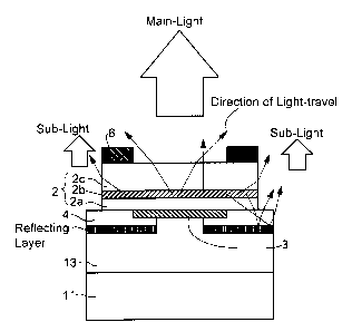
The semiconductor light-emitting element includes the first terminal 3, the
laminated semiconductor layer 2 with the light-emitting layer, and the second
terminal 6 on or above the supporting substrate 11 successively. Here, the
first
terminal 3 is provided in the junction plane side with the supporting
substrate 11
supporting the semiconductor layer 2. In addition, the second terminal 6 is
provided the light-outgoing surface side of the semiconductor 2. In such
light-emitting element, the light emitted from the light-emitting layer is not
radiated
only upward, or toward outgoing surface, but also in all direction. So that
the light
radiated downward in the light emitted from the light-emitting layer is
absorbed by
the other formed layers. On the other hand, the thickness of the semiconductor
layer 2 formed in the semiconductor element is about several pm to 10 pm,
while
the length of the traverse direction is not less than 200 pm, further more
than 1
mm in wider one. Since the light transmitted longer distance until reflected
at the
side surface of the semiconductor, and so on, in the traverse direction than
in the
vertical direction, it is absorbed by the materials composing the
semiconductor.
Thus, the outgoing-efficiency of the light is reduced.
-10-
CA 02466141 2011-07-15
The semiconductor light-emitting element of the invention has: at least the
conductive layer 13; the first terminal 3; the semiconductor 2, which includes
the
first conductive type semiconductor layer 2a in the contact boundary side with
the
first terminal, the light-emitting layer thereon, and the second conductive
type
semiconductor layer 2c further thereon in the light-outgoing surface side; and
the
second terminal on or above the supporting substrate 11 successively. The
semiconductor light-emitting element further has the first protect layer 4,
which
has a contact boundary region with the semiconductor 2 and/or a region
extending from the contact boundary in traverse direction of the semiconductor
2.
It is meant also to include even interposing an interposition layer between
the first protect layer 4 and the semiconductor 2 that the first protect layer
4 has
the contact boundary region with the semiconductor 2, as long as the first
protect
layer 4 and the laminated semiconductor layer 2 has optical connection
transmittable of the light. Additionally, in the first protect layer 4, the
region
extending from the contact boundary in traverse direction of the semiconductor
2
is shown the region, in which the protect layer 4 is not in contact with the
semiconductor 2, extended to the outside of the semiconductor layer 2 (Fig.
3C,
3E, 3F, 4C, etc.). The first protect layer 4 is only to required to have the
effect as a
light-transmitting layer transmittable of the light emitted from the light-
emitting
layer. In addition, it works as insulating layer with the effect for
preventing a leak
current and for current convergence (current blocking). The light is
transmitted
from the light-emitting layer 2b downward, and moves into the first protect
layer 4.
The transmitted light is reflected upward at the boundary with a layer having
reflection effect, and outgoes as an outgoing light through the extending
region,
which is provided outside of the semiconductor layer 2 as a light-outgoing
surface.
-11-
CA 02466141 2011-07-15
The light transmitted from the light-emitting layer 2b of the semiconductor 2
moves into the first protect layer 4, and it is repeatedly reflected at the
side
surfaces and the bottom surface of the first protect layer 4, then most of the
light
outgoes as the outgoing light upwardly though the top surface of the extending
region. The thickness of the first protect layer is less than the thickness of
the
semiconductor in growth direction. Thus, the absorption and loss in the
light-emitting element can be reduced, and the outgoing efficiency of the
light from
the light-emitting element is improved. It is preferable to select a material
with low
absorption coefficient as the first protect layer 4. The extending region,
which is a
light-outgoing path transmitting the light moving into the first protect layer
4
connected optically with the semiconductor layer 2, has the effect of guiding
the
emitted light outward before the light reflected repeatedly inside of the
semiconductor laminated body is absorbed caused of the internal absorption.
The
sub light, which outgoes from the extending region corresponding to outside of
the
semiconductor light-emitting element, is added to the main light, which
outgoes
from the upper part of the first terminal 3, so that the external quantum
efficiency
can be improved. Concretely, the conductive layer 13 works as the layer with
reflection effect, however, it is preferable to interpose a reflecting layer
between
the first protect layer 4 and the conductive layer 13. It is possible to
reduce the
loss at the reflection in the first protect layer 4.
Forming an asperity surface on the top surface of the extending region in
the first protect layer 4 by etching and so on can improve the outgoing
efficiency
of the light from the surface. As another constitution, forming a protect
layer 40
with refractive index n3 on the top surface of the extending region can also
achieve the same result. When the refractive index difference between the
formed
-12-
CA 02466141 2011-07-15
protect layer 40 and the refractive index n2 of the first protect layer 4 is
less than
the refractive index difference between the refractive index ni of the
semiconductor layer 2 and the refractive index n2 of the first protect layer
4, a
large part of the light outgoes toward less refractive-index-difference side.
Therefore, a large part of the light moves into the first protect layer 4
having the
surface exposed outside, and it is possible to improve the outgoing efficiency
of
the light.
Further, in the semiconductor light-emitting element, at least one first
terminal 3 and the first protect layer 4 is formed by turns on the surface of
the
semiconductor in the supporting substrate side. It is preferable that the
semiconductor light-emitting element has a reflecting layer under the first
protect
layer 4 (Fig. 12D). The light from the light-emitting layer is reflected at
the
boundary a between the first conductive type semiconductor layer 2a and the
first
terminal 3. In addition, the light-emitting layer passes through the boundary
between the first conductive type semiconductor layer 2a and the first protect
layer 4, and the light from the light-emitting layer is reflected at the
boundary b
between the first protect layer 4 and the conductive layer 13. The first
terminal 3
absorbs the light. To reduce this absorption of the light, reducing the
reflectivity at
the boundary between the semiconductor 2 and the first protect layer 4, and
increasing the reflectivity at the boundary b guides the light into the first
protect
layer 4, thereby the reflecting layer or the conductive layer 13 formed under
the
first protect layer reflects the light (Fig 12E). Thus, it is possible to
improve the
outgoing efficiency of the light. It is preferable that the reflectivity of
the first
protect layer 4 is lower than the first terminal 3, and is formed of a
material with
high transmittance of the light.
-13-
CA 02466141 2011-07-15
Both of the boundary a between the first conductive type semiconductor
layer 2a and the first terminal 3, and the boundary b between the first
protect layer
4 and the conductive layer 13 are formed as an asperity portions. Here, the
boundaries a, b are the surfaces with the effect as the light-reflecting
surface
reflecting the light from the light-emitting layer 2b. The first protect layer
4 is a
transparent layer. However, the first terminal 3 in contact with the side
surface of
the first protect layer 4 and the boundary b with the conductive layer 13 in
contact
with the back surface of the first protect layer 4 can reflect the light.
Recess
portions as the boundaries b and projecting portions as the boundaries a are
provided in traverse direction (Fig. 12D). It is appreciated that the
reflecting layer
shown in Fig. 12D, etc. may be omitted.
Providing the asperity portion can improve the outgoing efficiency of the
light from the semiconductor to the outside. The reasons is that the light,
which is
transmitted downward originally, is reflected or scattered with increasing the
vertical component of the transmittance. That is, the light is scattered at
the
asperity portion so as to run upward before it is transmitted for long
distance in the
traverse direction. Most of the light with the high traverse component of the
transmittance is absorbed in the semiconductor. However asperity portion
scatters the light from the light-emitting layer in all directions
divergently, then can
change the light with vertical component of the transmittance. Optical
connection
between such asperity portion and the extending region of the first protect
layer 4
as mentioned above further can improve the outgoing efficiency of the light.
The first terminal 3 and the first protect layer 4 are provided under the
same surface of the first conductive type semiconductor layer 2a. Here, while
the
first conductive type semiconductor layer 2a may have the bumps and dips of
the
-14-
CA 02466141 2011-07-15
asperity formed by "as-grown" or suitable micro process on the
first-terminal-forming surface, it is preferable that the surface is flat. If
the asperity
portion is formed on the semiconductor by etching, the semiconductor has not
some little damage. Accordingly, the life characteristics shall be reduced. In
the
invention, the asperity portion is not formed by etching, but also formed by
combining materials. Therefore, the outgoing efficiency of the light can be
improved without etching damage or reduction of the life characteristics.
The first protect layer 4 has a multi-layer structure composed of at least
two layers. The boundary surface between the layers is formed in asperity
surface.
It is preferable that the asperity surface is inclined. The first protect
layer 4 has the
area in the semiconductor larger than the first terminal 3 in the traverse
direction
of the semiconductor 2. Accordingly, the light transmitted in the first
protect layer
is high ratio of the whole emitted light. It is very important to change the
light,
which moves into the first protect layer 4 once, upward, thereby the light
outgoes.
To achieve it, forming the first protect layer 4 in the multi-layer structure
composed
of at least two layers, and forming the asperity in the first protect layer 4
scatter
the light, which moves into the first protect layer 4, at the boundary to
change its
direction upwardly. The first protect layer is composed of materials such as
SiO2,
A1203, ZrO2, TiO2, Nb2O5. For example, the first protect layer 4 is formed in
a
two-layer structure composed of Nb2O5 in the boundary side 4b, and SiO2 as a
lower the layer 4a. The asperity portion is provided between the two layers to
effect diffusion in the protect layer (Fig. 12F).
The nitride semiconductor element of the invention has the first terminal 3
and the second terminal 6 of the opposed terminal structure (Fig, 3, Fig. 12,
etc.).
As mentioned above, it is preferable that the second terminal is disposed on
the
-15-
CA 02466141 2011-07-15
portion corresponding to rest of the position, on which the first terminal is
disposed, however, it is not specifically limited, for example, the second
terminal
may be disposed on the portion corresponding to the first terminal portion
partially.
In Fig. 3D, when the second terminal 6 is an n-type terminal, the current
flows in
wide area of the nitride semiconductor in the second terminal side, or n-type
nitride semiconductor 2c. On the other hand, the current flows in narrow area
of
the nitride semiconductor in the first terminal 3 side, or p-type nitride
semiconductor 2a, so that the first terminal is widely formed in the surface
of the
nitride semiconductor. To achieve efficient outgoing of the light, it is
preferable that
the second terminal is formed in a shape surrounding the top surface of the
light-outgoing portion of the semiconductor 2. However, the terminal-forming
area
of the second terminal 6 can be small, both terminals may partially overlap
each
other as long as no cutting off a large amount of the light (Fig. 12E).
In addition, in the invention, the bumps and the dips of the asperity portion
formed in the light-outgoing surface are formed in square shapes or
rectangular
shapes with square corners, mesa shapes or reverse-mesa shapes with inclined
surfaces, or the like. It is preferable that the shape of the asperity portion
has
inclined surfaces.
The semiconductor 2 is nitride semiconductor in the invention. The nitride
semiconductor is a semiconductor compound including nitrogen. The nitride
semiconductor is direct-band-gap semiconductor. It has efficiency of
light-emission much higher than indirect-band-gap semiconductor. Additionally,
when it is formed of a semiconductor compound including group III element such
as In, Ga, Al, the semiconductor light-emitting element capable of light-
emission
in the short wavelength region (300-550 nm) including ultra-violet region can
be
-16-
CA 02466141 2011-07-15
provided.
The light-emitting layer has a quantum well structure, which includes at
least a well layer of AlalnbGal_a_bN (0:5a:51, 05b:51, a+b:51) and a barrier
layer of
AlclndGa,_o_dN (0_<c<1, 0<d<1, c+d<1). The quantum well structure can provide
the
light-emitting element with high light-emission efficiency. The quantum well
structure can be either a single quantum well structure or multi-quantum-well
structure. In addition, it is preferable for achieving high power that b of
the In
composition of the well layer is set as 0<b<_0.3. Because the mixture ratio b
of In is
higher, the crystallinity is prone to be uneven in the plane cause of
segregation of
the crystal, and preferable portions are interspersed in the plane.
Additionally, it is
prone to makes less linearity of the current-output characteristics and to
become
saturated easily. However, setting within the above range of the In
composition
can apply a large amount of current, so that it provide the advantage in the
invention.
The light-emitting layer has a quantum well structure, which includes at
least a well layer of AlalnbGa1_a_bN (0<a:51, 0<b:51, a+b<1) and a barrier
layer of
AlclndGa,_c_dN (0<c:51, 0<d!51, c+d<1), and the first conductive type
semiconductor
layer is disposed in one side of the principal plane of the light-emitting
layer, the
second conductive type semiconductor layer, which includes Al, is disposed in
another side of the principal plane of the light-emitting layer. In addition,
in the
range not more than 420 nm (near-ultra-violet region), which is low
luminosity, b of
the In composition is set as around 0<b<0.1. In the range not more than 380 nm
(ultra-violet region), a of the Al composition is set as around 0.01:5b:50.2.
The second conductive type nitride semiconductor layer includes at least
two layers, one layer of said two layers, which is disposed in the second
terminal
-17-
CA 02466141 2011-07-15
side, is formed of AleGa,-,N, and another layer of said two layers, which is
disposed in the light-emitting layer side, is formed of AlfGa,_fN, wherein,
the
impurity concentration of the AleGa,_eN layer is higher than the AlfGa,_fN
layer.
In the invention, AlalnbGaI_a_bN (0:5as1 0:5b51, a+b<_1) can be employed as
an active layer of the nitride semiconductor element. It can be applied to
elements
emitting light with various wavelengths, in the light-emitting element of
InAIGaN
system. Especially, the nitride semiconductor element in the ultra-violet
region,
which is not more than 380nm, further has a particular advantageous. The
invention provide a method for producing the nitride semiconductor element,
which has a active layer having a quantum well structure with a well layer
formed
of a quaternary mixed crystal of InAIGaN and a barrier layer formed of nitride
semiconductor including at least Al, capable of use even for short wavelength
range, which is not more than 380 nm, appropriately. Because the well layer of
the
above active layer is formed of a quaternary mixed crystal of InAlGaN, it can
minimize the number of the composition elements, and can reduce deterioration
of the crystallinity, and further can improve light-emission efficiency. In
addition,
the band gap of the barrier layer formed of the nitride semiconductor
including at
least Al can be wider than the well layer, so that the active layer with the
quantum
well structure suitable for the wavelength of the light-emission can be
formed, and
can be maintain preferable crystallinity in the active layer.
Further, especially in the nitride semiconductor element for the ultra-violet
region, which is not more than 380nm, it is required to grow a GaN layer on or
above a substrate, a buffer layer at high temperature for obtaining the
nitride
semiconductor element with preferable crystallinity. If a light-emitting layer
(active
layer) is grown without growing this layer, its crystallinity may be very
poor.
-18-
CA 02466141 2011-07-15
Therefore, in such nitride semiconductor light-emitting element, its light-
emitting
power is quit low, so that it is not appropriate for practical use. Thus,
forming a
high-temperature-grown layer of GaN can provide the nitride semiconductor
element with preferable crystallinity. However, when a GaN layer is included
as a
primary layer or the high-temperature-grown layer, this GaN layer absorbs a
part
of the light from the active layer cause of the self-absorption of the GaN in
the
ultra-violet region. In the invention, the substrate for growing, the buffer
layer, and
high-temperature-grown layer of GaN are eliminated after attaching the
conductive substrate, so that it can maintain the crystallinity of the nitride
semiconductor element appropriately, and can reduce self-absorption.
It should be appreciated that a composition-graded layer may further be
formed on or above the high-temperature-grown layer. The composition-graded
layer is useful for the LED, which does not have GaN playing a role of
recovering
crystallinity, capable of emitting in ultra-violet region. It can laminate the
nitride
semiconductor layer with less defect and high crystallinity. In addition, It
should be
appreciated that the composition-graded layer may be formed with
modulated-doping so as to grade impurity concentration affecting its
conductivity.
When the nitride semiconductor layer of Si-doped AIGaN is formed thereon for
example, the composition-graded layer is formed in the structure graded from
undope to the impurity concentration similar to the Si-concentration of the n-
type
cladding layer. It can laminate the nitride semiconductor layer with further
less
defect and high crystallinity. Additionally, it should be appreciated that the
composition-graded layer may be formed with graded from a
high-impurity-concentration region to an undoped layer.
-19-
CA 02466141 2011-07-15
In the nitride semiconductor element of the invention, especially in the
light-emitting element, it should be appreciated that a coating layer or a
molding
material including a fluorescent material, which can absorb a part of or the
whole
of the light from the active layer then can emit light with different
wavelength, may
be formed on the nitride semiconductor element with attached to supporting
substrate. It can emit light with various wavelengths. Examples of the
fluorescent
material are shown as follows. SrA1204:Eu; Y2SiO5:Ce,Tb; MgAl11O19:Ce,Tb;
Sr7AI12O25:Eu; and (at lease one element selected from the group of Mg, Ca,
Sr,
and Ba)Ga2S4:Eu are can be employed as a greenish fluorescent material. In
addition, Sr5(P04)3C1:Eu; (SrCaBa)5(PO4)3CI:Eu; (BaCa)5(PO4)3CI:Eu; (at lease
one element selected from the group of Mg, Ca, Sr, and Ba)2B5O9CI:Eu,Mn; and
(at lease one element selected from the group of Mg, Ca, Sr, and
Ba)(P04)6CI2:Eu,Mn can be employed as a bluish fluorescent material.
Additionally, Y202S:Eu; and La202S:Eu; Y203:Eu; Gd202S:Eu are can be
employed as a reddish fluorescent material. Especially, including YAG can emit
white light, so that it can be applied to a light source for illumination,
etc. widely.
The YAG is represented in (Y1_,Ga,)3(AI1_yGay)5O12:R (R is at lease one
element
selected from the group of Ce, Tb, Pr, Sm, Eu, Dy, and Ho. 0<R<0.5.), for
example (Yo.8Gd0.2)3AI5O12:Ce or Y3(AIo.8Ga0.2)5O12:Ce or the like. In
addition, with
regard to the fluorescent material, which can absorb a part of or the whole of
the
light then can emit light with different wavelength; the material, which can
absorb
a part of or the whole of visible light then can emit light with different
wavelength,
is limited. Therefore, there is a problem of material selectivity. However,
many
materials, which can absorb a part of or the whole of the ultra-violet light
then can
emit light with different wavelength, are known, so that it can select the
material
-20-
CA 02466141 2011-07-15
according to various applications. One reason to be able to select the
material is
high efficiency of light-conversion of the fluorescent material absorbing
ultra-violet
light compared with the efficiency of light-conversion of visible light. White
light
widely provides possibility such as obtaining white light with high color
rendering
or the like. The invention can provide a nitride semiconductor light-emitting
element with less self-absorption. Further, the invention can provide a white
light-emitting element with extremely high efficiency of conversion by coating
the
fluorescent material.
(Fluorescent Material)
The above fluorescent material used in the invention is described in more
detail below. It is preferable that the fluorescent material has particle size
with
center particle size in the range of 6-50 pm. It is more preferable that the
center
particle size is in the range of 15-30 pm. The fluorescent material with such
particle size has a high absorption coefficient, high converting efficiency,
and wide
range of excited light wavelength. Since the fluorescent material with the
particle
size less than 6 pm relatively tends to form aggregate, they sediment in the
liquid
resin cause of their density, so that it might reduces transmittance of the
light,
further, its absorption coefficient and the converting efficiency might be
poor, and
its range of excited light wavelength might be narrow.
In the invention, the particle size is meant a value obtained by the
volume-base particle size distribution curve. The volume-base particle size
distribution curve is measured by the laser diffraction and scattering method.
Specifically, it can be obtained with measurement of sodium hexametaphosphate
aqueous solution, in which each substance is dispersed, with 0.05%
concentration by laser diffraction type particle size distribution analyzer
-21-
CA 02466141 2011-07-15
(SALD-2000A), in the measurement particle size range 0.03 pm-700 pm, under
circumstance temperature 25 C and humidity 70%. In the invention, the center
particle size is meant a particle size value when the integrated value reaches
50%
in the volume-base particle size distribution curve. It is preferable that the
content
of the fluorescent material with this center particle size is high. It is
preferable its
content is 20-50%. Employing the fluorescent material with less variation of
the
particle size can reduce variation of the color, so that the light-emitting
device
with preferable contrast can be provided.
(Yttrium-Aluminum-Oxide System Fluorescent Material)
The light-emitting device of the invention employs a fluorescent material
based on the yttrium-aluminum-oxide based fluorescent material (YAG system
fluorescent material) activated with cerium (Ce) or praseodymium (Pr), which
can
light with being exited by the light emitted from the semiconductor light-
emitting
element with the light-emitting layer of the nitride semiconductor.
As the concrete yttrium-aluminum-oxide based fluorescent material,
YAIO3:Ce, Y3AI5012:Ce(YAG:Ce), Y4A1209:Ce, or mixture of them may be usable.
The yttrium-aluminum-oxide based fluorescent material may include at least one
element selected from the group consisting of Ba, Sr, Mg, Ca, and Zn. In
addition,
adding Si can control or reduce reaction of the crystal growth to make
particles of
the fluorescent material uniform.
In this specification, the yttrium-aluminum-oxide based fluorescent
material activated with cerium is meant in a broad sense, and it includes a
fluorescent material capable of fluorescent action having at least one element
selected from the group consisting of Lu, Sc, La, Gd, and Sm, with which
substitute all or part of the yttrium and/or at least one element selected
from the
-22-
CA 02466141 2011-07-15
group consisting of Ba, TI, Ga, and In, with which substitute all or part of
the
aluminum.
More specifically, it may be a photo-luminescent fluorescent material
having a general formula (YZ Gd, _ Z )3 Al5 O, 2 :Ce (where 0<z<=1), or a
photo-luminescent fluorescent material having a general formula
(Re, -a Sma )3 Re'5 012 :Ce (where 0<=a<1; 0<=b<1; Re is at least one element
selected from the group consisting of Y, Gd, La, and Sc; and Re' is at least
one
element selected from the group consisting of Al, Ga, and In.). Since the
fluorescent material has a garnet stricture, it is impervious to heat, light,
and
moisture. Its peak of excitation spectrum can be around 450 nm. The peak of
light-emission is around 580 nm, and the distribution of the light-emission
spectrum is broad in which the foot of the distribution extends to about 700
nm.
Gd (gadolinium) may be added to the crystal lattice of the
photo-luminescent fluorescent material to improve excited light-emission
efficiency in the long-wavelength range over 460 nm. Increasing the Gd content
shifts the peak wavelength of the light-emission toward long-wavelength side,
and
also overall wavelength of the light-emission toward long-wavelength side. In
other words, if reddish light-emission color is needed, increasing the amount
of
substitutive Gd can achieve it. On the other hand, the more Gd is increasing,
the
less luminance of the photo-luminescent by the blue light. Other elements such
as Tb, Cu, Ag, Au, Fe, Cr, Nd, Dy, Co, Ni, Ti, Eu may be added as well as Ce,
if
desirable. If Al in the composition of the yttrium-aluminum-garnet fluorescent
material with the garnet structure is partially substituted with Ga, the
wavelength
of the light-emission shifts toward longer-wavelength region. In contrast, if
Y in the
composition is partially substituted with Gd shifts the wavelength of the
-23-
CA 02466141 2011-07-15
light-emission toward longer-wavelength region.
If a part of Y is substituted with Gd, it is preferable that the percentage of
substitutive Gd is less than 10%, and the composition ratio or substitution is
0.03-1Ø In case the percentage of substitutive Gd were less than 20%, the
light
in the green range would be high and the light in the red range be less.
However,
increasing content of the Ce can compensate the light in the red range, so as
to
be desired color tone without reduction of the luminance. Such composition can
achieve preferable temperature characteristics, and improve reliability of.
the
light-emitting diode. In addition, to use the photo-luminescent fluorescent
material
adjusted to emit the light in the red range, the light-emitting device can
emit the
intermediate color such as pink.
A material for the photo-luminescent fluorescent material can be obtained
by mixing oxides or compounds sufficiently, which can become oxide at high
temperature easily, as materials of Y, Gd, Al, and Ce according to
stoichiometry
ratio. The mixed material also can be obtained by mixing: coprecipitation
oxides,
which are formed by firing materials formed by coprecipitating solution
dissolving
rare-earth elements, Y, Gd, and Ce, in acid according to stoichiometry ratio
with
oxalic acid; and an aluminum oxide. After mixing the mixed material and an
appropriate amount of fluoride such as barium fluoride, ammonium fluoride as
flux,
inserting them in to a crucible, then burning them at temperature 1350-1450 C
in
air for 2-5 hours, as a result, a burned material can be obtained. Next, the
burned
material is crushed in water by a ball mill. Then washing, separating, drying
it,
finally sifting it through a sieve, the photo-luminescent fluorescent material
can be
obtained.
In the light-emitting device of the invention, the photo-luminescent
-24-
CA 02466141 2011-07-15
fluorescent material may be a substance mixed two or more kinds of the
yttrium-aluminum-garnet fluorescent material activated with cerium, or can be
a
substance mixed the yttrium-aluminum-garnet fluorescent material activated
with
cerium and the other fluorescent materials. Mixing two kinds of the
yttrium-aluminum-oxide system fluorescent materials, which have different
amount of the substitution from Y to Gd, can achieve the desired color light
easily.
Especially, when the fluorescent material with higher content of the amount of
the
substitution is the above fluorescent material, and the fluorescent material
with
lower content of or without the amount of the substitution is the fluorescent
material with middle particle size, both the color rendering characteristics
and the
luminance can be improved.
(Nitride System Fluorescent Material)
The fluorescent material used in the invention is a nitride system
fluorescent material, which includes N, and can include at least one element
selected from the group consisting of Be, Mg, Ca, Sr, Ba, and Zn, at least one
element selected from the group consisting of C, Si, Ge, Sn, Ti, Zr, Hf, and
is
activated with at least one element selected from the group consisting rare-
earth
elements. In the invention, the nitride system fluorescent material is meant a
fluorescent material, which is capable of absorbing the visible, ultra-violet
light
emitted from the light-emitting element, or the fluorescence from the YAG
fluorescent material partially and of emitting a excited light. The
fluorescent
material according to the invention is silicon nitride such as Mn-added
Sr-Ca-Si-N:Eu; Ca-Si-N:Eu; Sr-Si-N:Eu; Sr-Ca-Si-O-N:Eu; Ca-Si-O-N:Eu; and
Sr-Si-O-N:Eu systems. The basic component elements of the fluorescent material
is represented in the general formulas LXS1yN(2/3X+4/3Y):Eu or
-25-
CA 02466141 2011-07-15
LXSiYOZN(2/3X+4/3Y-2/3Z):EU (where L is any one element of Sr, Ca, Sr, or Ca).
It is
preferable that X and Y in the general formulas are X=2, Y=5, or X=1, Y=7,
however, it is not specifically limited. As concrete basic component elements,
it is
preferable that fluorescent materials represented in Mn-added
(SrxCai-x)2Si5N8:Eu; Sr2Si5N8:Eu; Ca2Si5N8:Eu; SrxCai-XSi7N,o:Eu; SrSi7N1o:Eu;
and CaSi7N1o:Eu are employed. Here, the fluorescent material may include at
least one element selected from the group consisting of Mg, Sr, Ca, Ba, Zn, B,
Al,
Cu, Mn, Cr, and Ni. In addition, the invention is not limited in these
materials.
L is any one element of Sr, Ca, Sr, or Ca. The composition ratio of Sr and
Ca can be varied, if desirable.
Employing Si in composition of the fluorescent material can provide the
low cost fluorescent material with preferable crystallinity.
Europium, which is a rare-earth element, is employed as center of
fluorescent. Europium mainly has a divalent or trivalent energy level. The
fluorescent material of the invention employs Eu2+ as the activator against
the
base material of alkaline-earth-metal system silicon nitride. Eu2+ tends to be
subject to oxidation. Trivalent Eu2O3 is available on the market. However, 0
in
Eu2O3 available on the market is too active, it is difficult to obtain the
preferable
fluorescent material. It is preferable to use Eu2O3, from which 0 is removed
out of
the system. For example, it is preferable to use europium alone or europium
nitride. In addition, when Mn is added, it is not always required.
Added Mn accelerates diffusion of Eu2+, and improves light-emitting
efficiency such as light-emission luminance, energy efficiency, or quantum
efficiency. Mn is included in the material, or is added in the process as Mn
alone
or Mn compounds, then is burned with the material. In addition, after burned,
Mn
-26-
CA 02466141 2011-07-15
does not remain in the basic component elements or remains much less than the
original content even included. It is considered that Mn flies away in the
burning
process.
The fluorescent material includes at least one element selected from the
group consisting of Mg, Sr, Ca, Ba, Zn, B, Al, Cu, Mn, Cr, and Ni in the basic
component elements or with the basic component elements. These elements
have the effect increasing the particle size, or improve light-emitting
luminance. In
addition, B, Al, Mg, Cr, and Ni have the effect reducing persistence.
Such nitride system fluorescent materials is capable of absorbing the blue
light emitted from the light-emitting element partially and of emitting a
excited light
in the region yellow to red. Employing the nitride system fluorescent material
with
the YAG system fluorescent material in the above light-emitting device can
provide the light-emitting device capable of emitting a warm white color by
mixing
the blue light emitted from the light-emitting element and the light in the
region
yellow to red from the nitride system fluorescent material. It is preferable
that the
other fluorescent materials except the nitride system fluorescent material
include
the yttrium-aluminum-oxide system fluorescent materials activated with cerium.
Including the yttrium-aluminum-oxide system fluorescent materials can adjust
desired chromaticity. The yttrium-aluminum-oxide system fluorescent material
activated with cerium is capable of absorbing the blue light emitted from the
light-emitting element partially and of emitting an excited light in the
region yellow.
The blue light emitted from the light-emitting element and the yellow light of
the
yttrium-aluminum-oxide system fluorescent material are mixed. Mixing the
yttrium-aluminum-oxide system fluorescent material and the fluorescent
material
capable of emitting red light in the color converting layer, and combining
them with
-27-
CA 02466141 2011-07-15
blue light emitted from the light-emitting element can provide the light-
emitting
device emitting white light as mixed color light. It is preferable that its
chromaticity
of the white-light-emitting device is on blackbody radiation locus in the
chromaticity diagram. In addition, to provide a light-emitting device with
desired
color temperature, the amount of the yttrium-aluminum-oxide system fluorescent
material and the amount of the fluorescent material capable of emitting red
light
may be changed if desired. The light-emitting device emitting whitish mixed
light is
aimed at improving a special color-rendering index of R9. In a conventional
white-light-emitting device combining the bluish-light-emitting element and
the
yttrium-aluminum-oxide system fluorescent material activated with cerium, its
special color-rendering index of R9 around color temperature Tcp=4600 K in
nearly zero, and a red color component is not enough. Accordingly, it is
required
to improve special color-rendering index of R9. In the invention, employing
the
fluorescent material capable of emitting red light with the yttrium-aluminum-
oxide
system fluorescent material can improve special color-rendering index of R9
around color temperature Tcp=4600 K to about 40.
Next, a process for producing the fluorescent material
((SrxCai_x)2Si5N8:Eu) used in the invention will be described as follows.
However,
the process for producing in the invention is not specifically limited. The
above
fluorescent material includes Mn, 0.
1. The materials Sr and Ca are pulverized. It is preferable to use Sr and Ca
alone
as the materials. However, an imide compound, an amide compound, or the like
also can be employed. In addition, the materials Sr, Ca may include B, Al, Cu,
Mg,
Mn, A1203, and so on. The materials Sr and Ca are pulverized in the glove box
under atmosphere with argon. It is preferable that Sr and Ca have the average
-28-
CA 02466141 2011-07-15
particle size about 0.1 pm-15 pm, however it is not specifically limited. It
is
preferable that the purity of Sr and Ca is more than or equal to 2N, however
it is
not specifically limited. To achieve preferable mixture, at least one element
of
metal Ca, metal Sr, and metal Eu is alloyed, and nitrided, then pulverized for
using
as the materials.
2. The material Si is pulverized. It is preferable to use Si alone as the
materials.
However, a nitride compound, an imide compound, an amide compound, or the
like, for example Si3N4, Si(NH2)2, and Mg2Si, etc. also can be employed. It is
preferable that the purity of the material Si is more than or equal to 3N,
however
the material may include compounds such as AI2O3, Mg, metal boride (C03B,
Ni3B,
CrB), manganese oxide, H4B03, B203 Cu2O, and CuO. Si is also pulverized in the
glove box under atmosphere with argon or nitride, similar to the material Si
and
Ca. It is preferable that the Si compound has the average particle size about
0.1
pm-15 pm.
3. Subsequently, the materials Sr and Ca are nitrided under atmosphere with
nitrogen. The equations, as Equation 1 and Equation 2, are
3Sr+N2 -* Sr3N2 (Equation 1)
3Ca+N2 -> Ca3N2 (Equation 2)
Sr and Ca are nitrided under atmosphere with nitrogen at 600-900 C for about 5
hours. Sr and Ca are nitrided with mixed together, or are nitrided
individually.
Finally, a strontium nitride and a calcium nitride are obtained. It is
preferable that
the strontium nitride and the calcium nitride have high purity. However, a
strontium nitride and a calcium nitride on the market also can be employed.
4. The material Si is nitrided under atmosphere with nitrogen. The equation,
as
Equation 3, is
-29-
CA 02466141 2011-07-15
3Si+2N2 --> Si3N4 (Equation 3)
Silicon Si is also nitrided under atmosphere with nitrogen at 600-900 C for
about 5
hours. Finally, a silicon nitride is obtained. It is preferable that the
silicon nitride
used in the invention has high purity. However, a silicon nitride on the
market also
can be employed.
5. The strontium nitride and the calcium nitride, or the strontium-calcium
nitride is
pulverized. The strontium nitride, the calcium nitride, and the strontium-
calcium
nitride are pulverized in the glove box under atmosphere with argon or
nitrogen.
The silicon nitride is pulverized similarly. In addition, the europium
compound Eu2O3 is also pulverized similarly. Here, the europium oxide is
employed as the europium compound, however metal europium, a europium
nitride, or the like, can be employed. An imide compound, an amide compound,
or
the like can be employed as the material Z. It is preferable that the europium
oxide
has high purity. However, the europium oxide on the market also can be
employed. It is preferable that the alkaline-earth-metal nitride, the silicon
nitride,
and the europium oxide have the average particle size about 0.1-15 pm.
The above materials may include at least one element selected the group
consisting of Mg, Sr, Ca, Ba, Zn, B, Al, Cu, Mn, Cr, 0, and Ni. In addition,
the
above elements such as Mg, Zn, and B may be mixed with adjusting content in
the
processes below. These compounds can be added in the materials alone,
normally they are added in the form of compounds. Such compounds are H3B03,
Cu2O3, MgCI2, MgO=CaO, A12O3, metal boride (CrB, Mg3B2, AIB2, MnB), B203,
Cu2O, CuO, and so on.
6. After pulverized, the strontium nitride, the calcium nitride, and the
strontium-calcium nitride, the silicon nitride, and the europium compound
Eu2O3
-30-
CA 02466141 2011-07-15
are mixed, and added with Mn. Since these mixtures undergo oxidation easily,
they are mixed under atmosphere with argon or nitrogen in a glove box.
7. Finally, the mixtures of the strontium nitride, the calcium nitride, and
the
strontium-calcium nitride, the silicon nitride, and the europium compound
Eu2O3
are burned under atmosphere with ammonia. Burning them can provide the
fluorescent material represented in formula Mn-added (SrxCa,_x)2Si5N8:Eu. In
addition, the ratio of each material can be changed so as to obtain
composition of
the desirable fluorescent material.
A tube furnace, a small furnace, a high-frequency furnace, a metal
furnace, or the like can be used for burning. The burning is performed at
burning
temperature in the range 1200-1700 C, however it is preferable that the
burning
temperature is at 1400-1700 C. It is preferable to use one-stage burning, in
which
temperature rises slowly and burning is performed at 1200-1500 C for several
hours. However, Two-stage burning (multi-stage burning), in which first-stage
burning is performed at 800-1000 C, and temperature rises slowly, then
second-stage burning is performed at 1200-1500 C, also can be used. It is
preferable that the materials of the fluorescent material are burned in a
crucible or
a boat of a boron nitride (BN) material. Instead of the crucible of a boron
nitride
material, a crucible of alumina also can be used.
The desired fluorescent material can be obtained by the above method.
The nitride system fluorescent material is used as the fluorescent material
capable of emitting reddish light in the light-emitting device as mentioned
above.
However, the light-emitting device can have the above YAG system fluorescent
material and the fluorescent material capable of emitting reddish light. Such
the
fluorescent material capable of emitting reddish light is a fluorescent
material,
-31-
CA 02466141 2011-07-15
which can emit excited light by the light with wavelength 400-600 nm, for
example
Y2O2S:Eu, La202S:Eu, CaS:Eu, SrS:Eu, ZnS:Mn, ZnCdS:Ag,Al, ZnCdS:Cu, Al,
and so on. Using the fluorescent material capable of emitting reddish light
with the
YAG system fluorescent material can improve color rendering o the light-
emitting
device.
Regarding the YAG system fluorescent material and the fluorescent
material capable of emitting reddish light, for representative example the
nitride
system fluorescent material, formed as mentioned above, one layer of the
color-converting layer in the side end surface of the light-emitting element
includes two or more kinds of them, or two layers of the color-converting
layer
include one or more kinds of them respectively. Such constitution can provide
mixed color light from different kinds of the fluorescent materials. In this
case, it is
preferable that each kind of the fluorescent materials has similar average
particle
size and similar shape for mixing the light from each kind of the fluorescent
materials, and for reducing color variation. In addition, since the light
converted its
wavelength by the YAG system fluorescent material is partially absorbed by the
nitride system fluorescent material, it is preferable that the nitride system
fluorescent material is provided in the position closer to the side end
surface of the
light-emitting element than the YAG system fluorescent material. Accordingly
the
light converted its wavelength by the YAG system fluorescent material can
avoid
to be absorbed partially by the nitride system fluorescent material.
Therefore, the
color rendering of the mixed light of the YAG system fluorescent material and
can
be improved compared with mixing both fluorescent materials together.
The method of the invention for producing a nitride semiconductor
element having at least a conductive layer, a first terminal, a nitride
semiconductor
-32-
CA 02466141 2011-07-15
with a light-emitting layer, and a second terminal, from a supporting
substrate
successively, comprising: a growing step for growing the nitride semiconductor
having at least a second conductive type nitride semiconductor layer, the
light-emitting layer, and a first conductive type nitride semiconductor layer,
on a
different material substrate; subsequently, an attaching step for attaching
the
supporting substrate to the first conductive type nitride semiconductor layer
side
of the nitride semiconductor with interposing the first terminal between them;
and
subsequently, a different-material-substrate-eliminating step for eliminating
the
different material substrate so as to expose the second conductive type
nitride
semiconductor layer. When an n-type layer, a p-type layer of the nitride
semiconductor layer are formed on the different material substrate
successively,
eliminating the different material substrate (sapphire, etc.) after attaching
the
supporting substrate exposes the surface of the n-type layer. A damaged layer
is
formed in the surface of the n-type layer by eliminating the different
material
substrate with polishing. However, the damaged layer can be eliminated by
chemical polishing, therefore eliminating the different material substrate may
not
reduce its characteristics.
The conductive layer is formed by a eutectic junction in the attaching step.
The attaching step is performed by thermocompression bonding. It is preferable
that the temperature is 150-350 C. In the case more than or equal to 150 C, it
can
accelerate diffusion of the metal of the conductive layer, so that the
eutectic with
uniform density distribution can be formed. Thus, It can improve intimate
contact
between the nitride semiconductor element and the supporting substrate. In the
case over the 350 C, the region of the diffusion may spread to the attaching
region, so that it may reduce the intimate contact. The eliminating step
eliminates
-33-
CA 02466141 2011-07-15
the different material substrate by laser irradiation, polishing, or chemical
polishing. The above step can make the exposed surface of the nitride
semiconductor element mirror-like surface.
The method further includes an asperity-portion-forming step for forming
an asperity portion on the exposed surface of the nitride semiconductor, which
is
the second type conductive nitride semiconductor layer, after the
different-material-substrate-eliminating step. It can make the emitted light
to be
diffused at the asperity portion. Therefore, the light, which had total
internal
reflection conventionally, can be directed upward, and can outgo to outside of
the
element.
The method further includes a step for forming a second insulating protect
layer on the exposed surface of the nitride semiconductor, which is the second
type conductive nitride semiconductor layer, after the
different-material-substrate-eliminating step. It can prevent short circuit
when
chipping by dicing, etc. to separate into chips. SiO2, TiO2, AI2O3, and ZrO2
can be
employed as the protect layer. The method further includes a step for forming
an
asperity portion on the second insulating protect layer. It is preferable that
the
refractive index of the second insulating protect layer is more than or equal
to 1
and not more than 2.5. Because the refractive index of the second insulating
protect layer is between the nitride semiconductor element and the air, the
outgoing efficiency of the light can be improved. It is more preferable that
it is
more than or equal to 1.4 and not more than 2.3. The constitution mentioned
above can achieve more than or equal to 1.1 times of the outgoing efficiency
of
the light as much as that without the protect layer. The protect layer also
can
prevent surface deterioration.
-34-
CA 02466141 2011-07-15
The method further includes a step for breaking the nitride semiconductor
into chips by etching the exposed surface of the nitride semiconductor after
the
different-material-substrate-eliminating step. In the light-emitting element
of the
invention, first, the semiconductor 2 is etched from the light-outgoing side
until the
first insulating layer 4, then the light-emitting element is formed into chips
on the
supporting substrate 11, to form the extending region of the first protect
layer 4. At
that time, though the semiconductor 2 is separated individually, the
supporting
substrate is not separated, in the wafer. Subsequently, the second insulating
protect layer 7 is formed on the semiconductor 2 and the extending region of
the
first protect layer 4 except wire-bonding region of the second terminal 6.
Forming
the second insulating protect layer 7 on the side surfaces and the top surface
of
the semiconductor 2 can reduce physical damages cause of electric shorting and
dust attachment. Next, after the second insulating protect layer 7 is formed,
the
light-emitting element is chipped by dicing from the supporting substrate 11
side.
Consequently, a chip of the light-emitting element is obtained.
Subsequently, the light-emitting device is formed. First, the light-emitting
element is mounted on a heat sink with lead frames, then conductive wires are
bonded from the light-emitting element to the lead frames. After that,
transparent
glass packages it, and the light-emitting device is obtained (Fig. 19).
In a light-emitting device as another example, a package resin with a heat
sink is prepared, and the light-emitting element is formed on the heat sink,
then
conductive wires are bonded from the light-emitting element to the lead
frames.
Subsequently, mold resin such as silicone is applied on the light-emitting
element.
Further, a lens is formed thereon, and the light-emitting device is obtained
(Fig.
20).
-35-
CA 02466141 2011-07-15
It is preferable that the light-emitting device has a protect element for
static protection of the light-emitting element.
The nitride semiconductor element of the invention includes a conductive
layer, a first terminal, a first conductive type nitride semiconductor layer
interposing the first terminal and a first insulating protect layer between
the
conductive layer and thereof, a nitride semiconductor with a light-emitting
layer,
and a second terminal, on or above a supporting substrate successively. The
nitride semiconductor element has a structure, in which the first terminal and
the
second terminal oppose each other. In addition, it is preferable that the
second
terminal is disposed on the portion corresponding to rest of the position, on
which
the first terminal is disposed. The nitride semiconductor layers except the
light-emitting layer in the nitride semiconductor have a band gap larger than
the
light-emission band gap.
EMBODIMENT 1
The following description will describe a process of producing of an
embodiment of the nitride semiconductor element according to the invention
with
the drawings.
The nitride semiconductor 2 including at least a second conductive type
nitride semiconductor layer, a light-emitting layer, a first conductive type
nitride
semiconductor layer is grown on a different material substrate 1 such as
sapphire
(Fig. 1A). Subsequently, a first terminal 3 (p-type terminal, for example) is
formed
on the nitride semiconductor layers. Next, a first insulating protect layer 4
is
formed on an opening portion, or an exposed portion of the nitride
semiconductor
-36-
CA 02466141 2011-07-15
(Fig. 113). Further, a conductive layer 5 for alloying at attachment is formed
(Fig.
1C). It is preferable that the conductive layer has a three-layer structure
composed of an intimate-contact, a barrier layer, and a eutectic layer. On the
other hand, a supporting substrate 11 is prepared. It is preferable that a
conductive layer 12 is also formed on the surface of the supporting substrate
(Fig.
2A). Subsequently, the nitride semiconductor element and the supporting
substrate are attached by thermocomression bonding (Fig. 2B). Each of attached
surfaces is alloyed as a conductive layer 13 after attaching. Then, the
different
material substrate is eliminated (Fig. 2C). After the different material
substrate is
eliminated, the nitride semiconductor layer is broken into chips, and a second
terminal is formed on an exposed portion of the second conductive type nitride
semiconductor layer (Fig.3A). It should be appreciated that asperity may be
formed on the exposed portion of the second conductive type nitride
semiconductor layer except the portion formed the second terminal (Fig. 4).
Subsequently, a second insulating protect layer covers the top surface of the
nitride semiconductor element except region for wire-bonding (Fig.3B, Fig.
4B),
and the nitride semiconductor element is obtained by dicing into chip. In
addition,
it should be appreciated that the second insulating protect layer may be
formed in
an asperity shape (Fig. 5, Fig. 11).
It is adequate that the different material substrate 1 is a substrate capable
of epitaxial growth for the nitride semiconductor 2, and the size or thickness
of the
different material substrate is not restricted especially. An insulating
substrate
such as sapphire with any one of C-facet, R-facet, or A-facet as a principal
surface, or spinel (MgA12 04); silicon carbide (6H, 4H, 3C); silicon; ZnS;
ZnO; Si;
GaAs; diamond; and an oxide substrate such as lithium niobate, gallium acid
-37-
CA 02466141 2011-07-15
neodymium, which are capable of lattice junction with nitride semiconductor,
can
be employed as the different material substrate. In addition, when having
enough
thickness (several tenspm) capable of device processing, a nitride
semiconductor
substrate such as GaN or AIN can be employed. The different material substrate
with off angle can be employed. It is preferable that the angle is 0.1-0.5
degrees,
and is more preferable that the angle 0.05-0.2 degrees, when sapphire with
C-facet is employed.
Further, the nitride semiconductor grown above the different material
substrate is grown with interposing a buffer layer between them. It is
preferable
that nitride semiconductor represented in the general formula AlaGa,_aN
(0:5a:50.8)
is employed, and it is more preferable that nitride semiconductor represented
in
AlaGai-aN (0sa50.5) is employed as the buffer layer. It is preferable that the
thickness of the buffer layer is 0.002-0.5 pm. It is more preferable that it
is
0.005-0.02 pm. In addition, it is further more preferable that it is 0.01-0.02
pm. It is
preferable that the temperature of growing the buffer layer is 200-900 C. It
is
more preferable that it is 400-800 C. Thus dislocation or pits on the nitride
semiconductor can be reduced. Furthermore, it should be appreciated that
Al,,Ga1_,(N (0<_x!0) layer may be grown on the different material substrate by
the
ELO (Epitaxial Lateral Overgrowth) method. The ELO (Epitaxial Lateral
Overgrowth) method grows nitride semiconductor in lateral direction, and bends
pierced dislocation so as to converge, so that the dislocation is reduced.
An LED element of nitride semiconductor will be described in detail as
follows. After the buffer layer is grown at low temperature on the different
material
substrate, the second conductive type nitride semiconductor layer described
bellow is formed. It is preferable that a high-temperature-grown layer, which
is
-38-
CA 02466141 2011-07-15
grown at high temperature, is formed on the buffer layer. Undoped GaN or GaN
doped with n-type impurity can be employed as the high-temperature-grown
layer.
It is preferable to employ the undoped GaN for growing in high crystallinity.
It is
preferable that the thickness of the high-temperature-grown layer is more than
or
equal to 1 pm. It is more preferable that it is 3 pm. It is preferable that
the growing
temperature of the high-temperature-grown layer is 900-1100 C. It is more
preferable that it is more than or equal to 1050 C.
Consequently, an n-type contact layer is grown. It is preferable that the
composition AID Gal _j N (0<j<0.3), whose band gap is wider than the active
layer,
is formed as the -type contact layer. However the thickness of the n-type
contact
layer is not restricted especially, it is preferable that it is more than or
equal to 1
pm, and it is more preferable that it is more than or equal to 3pm. In
addition,
however the n-type impurity concentration of the n-type contact layer is not
restricted especially, it is preferable that it is 1X10¹⁷_ 1 X 10² /cm3 ,
and it is more
preferable that it is 1X10¹⁸_ 1 X 10' 9 /cm3. Additionally, the n-type
impurity
concentration can be graded. In addition, grading composition of Al can
provide
the effect as a cladding layer, which confines carrier.
The light-emitting layer (active layer) used in the invention has a quantum
well structure, which includes at least a well layer of AlalnbGa,_a_bN
(0:5a:51 0<b<1,
a+b!0) and a barrier layer of AIIndGal_c_dN (0<c<_1, 0<_d!51, c+d:51). It is
more
preferable that the well layer, the barrier layer are formed of AlalnbGal_a_bN
(0<a:51
0<b:51, a+b<1), AIcIndGal_c_dN (0<c<1, 0<d51, c+d<1) respectively. Any type of
Undope, n-type impurity doped, and p-type impurity doped nitride semiconductor
can be employed as the active layer. However it is preferable that the undoped
or
the n-type impurity doped nitride semiconductor is employed for the light-
emitting
-39-
CA 02466141 2011-07-15
element with high power. It is more preferable that the well layer is formed
in
undpoped and the barrier layer is formed in n-type impurity doped. It can
improve
the output and the efficiency of light-emission of the light-emitting element.
Including Al in the well layer can provide short wavelength, which is
difficult wavelength range to be obtained by the conventional well layer of
InGaN
and is around 365 nm of wavelength corresponding to the band gap of GaN
concretely
It is preferable that the thickness of the well layer is more than or equal to
1 nm and not more than 30nm. It is more preferable that it is more than or
equal to
2 nm and not more than 20nm. It is further more preferable that it is more
than or
equal to 3.5 nm and not more than 20nm. Because the well layer may not have
the effect appropriately, when it is less than 1 nm. Further, when it is more
than 30
nm, the crystallinity of quaternary of InAIGaN may be reduced, so that the
characteristics of the element may be reduced. In addition, when it is more
than or
equal to 2 nm, it can provide the layer with less unequal thickness and with
relative uniform layer-quality. Additionally, when it is not more than 20 nm,
it can
grow the crystal with reducing the occurrence of crystal fault. In addition,
when the
thickness is more than or equal to 3.5 nm, it can improve the output. Because
the
thickness of the well layer is increased, light-emitting recombination is
performed
in high light-emission efficiency and in high internal quantum efficiency
against
numbers of carriers as an LD driven by a larger amount of current. The effect
can
be achieved especially in a multi-quantum-well structure. When its thickness
is
more than or equal to 5 nm in a single quantum layer, the effect can be
achieved
for improving output as mentioned above. However the number of the well layers
is not restricted, when it is more than or equal to 4, it is preferable that
the
-40-
CA 02466141 2011-07-15
thickness of the well layers is not more than 10 nm so as to reduce the
thickness
of the active layer. Because when the thickness of each layer composing the
active layer is thick, the total thickness of the active layer should be
thick, so that it
is prone to increase Vf. It is preferable that the multi-quantum-well
structure has at
least one well layer, whose thickness is in the above range, or not more than
10
nm. It is more preferable that the thickness of the all well layers is not
more than
nm, as mentioned above.
Further, it is preferable that the barrier layer is doped with p-type impurity
or n-type impurity, or undpoed, and is more preferable that it is doped with n-
type
10 impurity or undoped, similar to the well layer. For example, when n-type
impurity
is doped in the barrier layer, it is required that its concentration is at
least more
than or equal to 5x101 6 /cm3. It is preferable that it is more than or equal
to
5x'101 6 /cm3 and not more than 2X101 8 /cm3 in an LED, for example. In
addition, it
is preferable that it is more than or equal to 5X10¹⁷ /cm3 and not more than
1 X 10² 0 /cm3 , and is more preferable that more than or equal to 1x101 8/cm3
and
not more than 5X10¹⁹/cm3in a high-power LED, or LD. In this case, it is
preferable that the well layer does not include n-type impurity substantially,
or is
grown with undoped. In addition, when n-type impurity is doped in the barrier
layer,
all barrier layers in the active layer can be doped, or a part of them can be
doped
the rest of them can be undoped. Here, when a part of the barrier layers are
doped with n-type impurity, it is preferable that the barrier layers in the n-
type
layer side in the active layer is doped. For example, doping into the n-th
barrier
layer Bn (n is a positive integer.) from n-type layer side can inject
electrons into
the active layers effectively. So that it can provide the light-emitting
element with
high light-emission efficiency and high internal quantum efficiency. Regarding
to
-41-
CA 02466141 2011-07-15
the well layers, doping into the m-th well layer Wm (m is a positive integer.)
from
n-type layer side can also provide the effect similar to the barrier layers.
Additionally, doping both the barrier layer and the well layer can provide the
similar effect.
In the light-emitting element of the invention, it is required to employ
nitride semiconductor, whose band gap is wider than the well layer, as the
barrier.
Especially, when the wavelength of light-emission of the well layer is in the
range,
which is not more than 380 nm, it is preferable that quaternary crystal of
AIInGaN
represented in general formula Al, Ind Gal _ c _ d N (0<c:51, 05d:51, c+d<1)
or ternary
crystal of AIGaN is employed as the barrier layer. Al composition ratio c of
the
barrier layer is higher than Al composition ratio a of the well layer, or c >
a, and it
can provide sufficient band gap energy between the well layer and the barrier
layer, so that it can provide the light-emitting element having the quantum
well
structure with high light-emission efficiency. In addition, when the barrier
layer
includes In (d > 0), it is preferable that In composition ratio d is not more
than 0.1.
It is more preferable that it is not more than 0.05. If In composition ratio d
is more
than 0.1, the reaction between Al and In is accelerated at growing, so that
the
crystallinity may be reduced, and the layer can not be formed appropriately.
When
In composition ratio d is not more than 0.05, it can further improve the
crystallinity,
so that preferable layer can be formed.
Further, because the difference of the band gap energy is provided by Al
composition ratio mainly, and In composition ratio d of the barrier layer can
be
applied in wider composition ratio range compared with In composition ratio b,
it is
possible to set as d>_b. In this case, the critical thickness of the well
layer and the
barrier layer can be varied, so that it is possible to set the thickness
-42-
CA 02466141 2011-07-15
spontaneously. Therefore, the active layer with desired characteristics can be
designed. It is preferable that the thickness of the barrier layer is more
than or
equal to 1 nm and not more than 30nm, and is more preferable that it is more
than
or equal to 2 nm and not more than 20nm. Because when it is less than 1 nm, a
uniform layer cannot be formed, and it cannot have the effect as the barrier
layer
sufficiently. In addition, when it is more than 30 nm, the crystallinity may
be
reduced.
Subsequently, the first conductive type nitride semiconductor is formed on
the light-emitting layer. Here, a plurality of layers, which is p-type layers,
is formed.
First, it is adequate to form composition, whose band gap is wider than the
well
layer, capable of confinement of carriers as a cladding layer, however it is
not
restricted, Alk Gal _ k N (0 <_ k<1) can be employed, and it is preferable
that
Alk Gal - k N (0<k<0.4) is employed especially. However the thickness of the p-
type
cladding layer is not restricted especially, it is preferable that it is 0.01-
0.3 pm. It is
more preferable that it is 0.04-0.2 pm. It is preferable that the p-type
impurity of
the cladding layer is 1 x 10' 8_1X102 1 /cm3. It is more preferable that it is
1 X 10¹⁹ -
5X 10² 0 /cm3 .
When the p-type impurity concentration is in the above range, bulk
resistance can be reduced without reduction of the crystallinity. A single-
layer or a
multi-layer (supperlattice structure) can be used as the p-type cladding
layer. In a
multi-layer, the multi-layer is composed of the above Alk Gal - k N and the
nitride
semiconductor, whose band gap is smaller than that, preferably. For example,
In, Gal _, N (0s 1<1), Al, Gal -R, N (0:5m<1, m>I) can be employed as the
smaller
band gap layer, similar to the n-type cladding layer.
-43-
CA 02466141 2011-07-15
In the supperlattice structure, it is preferable that thickness of one layer,
or
the thickness of each layer composing the multi-layer, is not more than 100 A.
It is
more preferable that it is not more than 70 A. It is further more preferable
that it is
10-40 A. In addition, when the p-type cladding layer is composed of the larger
band gap layer and the smaller band gap layer, at least one of the a band gap
larger layer and the smaller layer can be doped with p-type impurity.
Additionally,
when both of the a band gap larger layer and the smaller layer are doped, the
amount of doping can be same, or can be different.
Subsequently, a p-type contact layer is formed on the p-type cladding
layer. Alf Gal - f N (0:1<1) can be employed as the p-type contact layer.
Especially,
forming Alf Gal _ f N (0sf<0.3) can provide preferable ohmic contact with the
first
terminal as an ohmic terminal. It is preferable that the p-type impurity
concentration is more than or equal to 1 X 101 7 /cm3 . I n addition, it is
preferable
that the p-type contact layer has composition grading structure, p-type
impurity
concentration is higher side and the mixed crystal ratio of Al is smaller in
the
conductive substrate therein. In this case, the composition of the composition
grading structure can be varied continuously, or can be varied
discontinuously, in
multi stages. For example, the p-type contact layer can include a first p-type
contact layer, which has high p-type impurity concentration and low Al
composition ratio and is contact with the ohmic terminal; and a second p-type
contact layer, which has low p-type impurity concentration and high Al
composition ratio. The first p-type contact layer can provide preferable
ohomic
contact. The second p-type contact layer can prevent self-absorption.
-44-
CA 02466141 2011-07-15
The nitride semiconductor is grown by metal-organic chemical vapor
deposition (MOCVD), halide vapor-phase epitaxy (HYPE), molecular beam
epitaxy (MBE), etc., in the invention.
Subsequently, when the nitride semiconductor is formed as n-type nitride
semiconductor layer, p-type nitride semiconductor layer successively, after
the
nitride semiconductor 2 is grown on the different material substrate 1 (Fig.
1A),
the wafer is reterieved up from a reactor, then it is annealed under
atmosphere
with oxygen at more than or equal to 450 C. Thus, hydrogen, which bond with
the
p-type nitride semiconductor layer, is removed, so that the p-type nitride
semiconductor layer with p-type conductivity is formed.
Subsequently, the first terminal capable of ohmic contact with the surface
of the p-type nitride semiconductor layer, or first conductive type nitride
semiconductor layer, is formed. The first terminal 3 can be formed of Ni, Au,
W, Pt,
Ti, Al, Ir, Rh, Ag, Ni-Au, Ni-Au-RhO, Rh-Ir, Rh-Ir-Pt, etc. It is preferable
that the
first terminal is formed of Rh, Ag, Ni, Au, etc., which have high
reflectivity. Then it
is annealed under atmosphere with oxygen. The thickness of the first terminal
is
0.05-0.5 pm.
Subsequently, a first insulating protect layer 4 is formed on an exposed
portion of the nitride semiconductor 2, on which the first terminal 3 is
formed (Fig.
113). A single-layer or a multi-layer such as SiO2, AI2O3, ZrO2, and T102 can
be
employed as the material of the first insulating protect layer. It should be
appreciated that a metal layer with high reflectivity such as Al, Ag, and Rh
may
further be formed on the attachment surface with the supporting substrate. The
metal layer increases the reflectivity, so that it can improve the outgoing
efficiency
-45-
CA 02466141 2011-07-15
of the light. Then, a conductive layer 5 formed of at least one element
selected
from the group of Au, Sn, Pd, and In is formed on the attachment surface with
the
supporting substrate (Fig. 1C). In addition, while forming the first terminal
with Ag
can improve the effect of outgoing of the light, it is prone that migration of
said Ag
occurs when operating under high temperature, high humidity. If the migration
occurs, a leakage current appears. Therefore, when Ag is employed as the first
terminal, RhO is formed as a first layer of the conductive layer 5 without
forming
the first insulating protect layer 4. When RhO is formed the whole surface, it
can
cover Ag. Thus, the migration of Ag can be reduced, and it can achieve the
effect
of outgoing of the light.
On the other hand, the supporting substrate 11 to be attached onto the
conductive-layer-forming surface of the nitride semiconductor is prepared
(Fig.
2A). Cu-W, Cu-Mo, AISiC, AIN, Si, SiC, Cu-diamond, etc., as a metal-ceramic
composite materials or the like, can be employed as a concrete material. For
example, its general formula can be represented as Cu.W,_,( (0:5x530),
CuXMo1_),
(0:5x:550). When AIN, which is an insulating material, is used as the
supporting
substrate, it has advantage for disposing the chip onto a circuit such as a
printed
board. In addition, using Si provide advantage for low cost and for chipping
with
ease. It is preferable that the thickness of the supporting substrate is 50-
500 nm.
Making the supporting substrate thinner in the above range can improve thermal
-46-
CA 02466141 2004-05-04
dissipation. Additionally, it should be appreciated that the attachment
surface with
the nitride semiconductor or the opposite surface of the supporting substrate
may
have asperity. It is preferable that it has a structure with an intimate
contact layer,
a barrier layer, and a eutectic layer in the attachment surface. It can
prevent
diffusion with the first terminal. These compose a conductive layer 12 in the
supporting substrate side. For example, a metal layer such as Ti-Pt-Au, Ti-Pt-
Sn,
Ti-Pt-Pd, Ti-Pt-AuSn, W-Pt-Sn, RhO-Pt-Sn, RhO-Pt-Au, RhO-Pt-(Au, Sn), etc. is
formed. The metal layer is alloyed by eutectic, and it becomes the conductive
layer 13 in a later process. In addition, it is preferable that the attachment
surface
metals of the supporting substrate side and the nitride semiconductor side are
deferent. Because they can be eutectic at low temperature, and its melting
point
can increase after eutectic.
Subsequently, the conductive-layer-forming surface of the supporting
substrate 11 and the conductive-layer-forming surface of the nitride
semiconductor element face each other, then thermocompression bonding is
performed (Fig. 2B). Heat more than or equal to 150 C is applied with press.
It is
preferable that both attachment surfaces of the supporting substrate side and
the
nitride semiconductor side have the intimate contact layer, the barrier layer,
and
the eutectic layer. The intimate contact layer is a layer for high intimate
contact
with the first terminal. It is preferable that it formed with any metal of Ti,
Ni, W, and
Mo. The barrier layer is a layer for preventing diffusion of the metal
composing the
eutectic layer into the intimate contact layer. It is preferable that Pt or W
is
employed. In addition, it should be appreciated that a Au layer with the
thickness
approximately 0.3 pm may be formed between the barrier layer and the eutectic
layer, for further preventing diffusion of the metal of the eutectic layer
into the
-47-
CA 02466141 2004-05-04
intimate contact layer. At attachment, (first terminal) / (Ti-Pt-AuSn-Pt-Ti) /
(supporting substrate, First terminal/RhO-Pt-AuSn-Pt-Ti) / (supporting
substrate),
(first terminal) / (Ti-Pt-PdSn-Pt-Ti) / (supporting substrate), (first
terminal) /
(Ti-Pt-AuSn-Pt-RhO) / (supporting substrate) is formed. Thus, it can form
alloy
with high peel strength. Forming the conductive layer with eutectic can attach
at
low temperature, and can provide high bond strength. Attaching at low
temperature can provide the effect for preventing the warpage.
Subsequently, the different material substrate is eliminated by laser
irradiation from the supporting substrate side, or grinding (Fig. 2C). After
the
different material substrate is eliminated, the desired layer, which is the
second
conductive type nitride semiconductor layer, is exposed by CMP process
(chemical mechanical polishing) for the exposed nitride semiconductor. In this
process, the GaN layer grown at high temperature is eliminated, so that the
influence of the absorption can also eliminated in the LED with light-emission
wavelength in the ultra-violet region. This process can remove a damaged
layer,
and can adjust the thickness of the nitride semiconductor layer and the
surface
roughness. Then, outer region etching is performed for chipping the nitride
semiconductor element by RIE, etc. so as to eliminate outer region of the
nitride
semiconductor layer.
Subsequently, a second terminal 6 is formed on the exposed portion of
the second conductive type nitride semiconductor layer (Fig.3A). When an n-
type
terminal is used as the second terminal, Ti-Al-Ni-Au, W-Al-W-Pt-Au, AI-Pt-Au,
etc.
can be employed. The thickness of the second terminal is 0.1-1.5 jim. In
addition,
it should be appreciated that the exposed surface the second conductive type
nitride semiconductor layer may be formed in asperity (dimple processing) by
RIE,
-48-
CA 02466141 2004-05-04
etc. (Fig. 4A). It is preferable that it is formed in the region except
surface formed
the second terminal thereon. The asperity can be formed in a mesa type or a
reverse-mesa type in a cross-sectional view, and can be formed in an island
shape, a grid pattern shape, a rectangular shape, or a polygonal shape in a
plan
view.
Subsequently, a second insulating protect layer 7 is formed so as to cover
the exposed surface except pad-terminal-forming region of the second terminal
(Fig.3B, Fig. 4B). An insulating layer such as SiO2, Nb2O5, A1203, ZrO2, TiO2,
etc.
can be employed as the second insulating protect layer. Then, the exposed
surface of the protect layer can be formed in asperity shape for improving the
outgoing efficiency of the light by RIE, etc. (Fig. 5). RIE or wet etching can
control
at of the order of 0.1 Nm for forming the asperity. The bumps of the asperity
shape
of the protect layer can be formed in a mesa shape, triangle shape, a half-
round
shape in a cross-sectional view. Thus, inclined faces are provided in the
bumps,
so that the probability of occurrence of diffusion can be increased. It is
preferable
that the taper angle in the inclined faces of the bumps is more than or equal
to 30
degrees and not more than 60 degrees. In addition, the protect layer can be
formed in an island shape, a grid pattern shape, a rectangular shape, or
polygonal
shape in a plan view.
When the light-outgoing surface of the second insulating protect layer is
formed in an asperity shape in a cross-sectional view, the light, which does
not
outgo cause of total internal reflection, can pass through with varied the
angle of
the light at the asperity face (the boundary face of the light-outgoing).
Therefore,
its outgoing efficiency of the light is more than or equal to 1.5 times as
much as
without the asperity in the protect layer. The asperity shape of the protect
layer of
-49-
CA 02466141 2004-05-04
the nitride semiconductor element is at least one shape selected from the
group
of a triangle shape, a half-round shape in a cross-sectional view. In
addition, when
its corner is rounded, the probability of diffusion can be increased, so that
it can
further improve the outgoing efficiency of the light. It is preferable that
the depth of
the dips of the asperity is 0.2-3 pm. It is more preferable that it is 1.0-1.5
pm.
Because when the depth of the dips of the asperity is less than 0.2 pm, it may
not
improve the outdoing efficiency of the light. On the other hand, when it is
deeper
than 3 pm, it may not provide the effect as the protect layer, though the
resistance
is not varied. Additionally, drawing out to form the asperity shape in a
circle shape
or a polygonal shape can also improve its power with maintaining low
resistance.
Forming the asperity shape to the protect layer on the nitride semiconductor
layer
can improve the outgoing efficiency of the light without increasing the
voltage.
Because the nitride semiconductor itself is not thinned by the process, its
resistance is not increased. Furthermore, the nitride semiconductor does not
have
any damage caused by etching directly. In addition, when the asperity process
is
performed to the protect layer, a fine processing can be performed with
selecting
the appropriate material for etching such as RIE (reactive ion etching), etc.
compared with when asperity process is performed to the nitride semiconductor
layer. Forming the above cross-sectional shape can occur diffusion
effectively. It
is preferable that the difference of the refractive index between the protect
layer
and the GaN is in the range 0.5. The constitution mentioned above can improve
more than or equal to 1.5 times of the outgoing efficiency of the light as
much as
without protect layer, without increasing the voltage. Additionally, the
protect layer
can provide the effect for preventing the surface deterioration. With the
insulative
protect layer, the short circuit can be prevent when chipping such as dicing
for
-50-
CA 02466141 2004-05-04
breaking into chips.
Subsequently, the nitride semiconductor element is broken into chips by
dicing, etc.
Fig. 18 is a graph showing current-output characteristics of an
embodiment of the invention with attached supporting substrate and a
conventional nitride semiconductor element with sapphire substrate. The
thermal
resistance of the nitride semiconductor element with the supporting substrate
is
low, so that more than or equal to 2000 mA of current can be applied, and it
can
output more than or equal to 350 mW. On the other hand, the thermal resistance
of conventional nitride semiconductor element with sapphire substrate is high,
so
that the thermal dissipation is low. Therefore, it cannot perform high output.
Here,
both of the nitride semiconductor elements and terminals are same condition.
Another nitride semiconductor light-emitting element of the embodiment 1
will be described as follows. It has a conductive layer, a first terminal, a
first
conductive type nitride semiconductor layer, nitride semiconductor, on or
above a
supporting substrate successively. It has a second terminal on the nitride
semiconductor. Pad terminal forming regions are formed at corners in the
diagonal line of the four corners, the second terminal with a mesh shape is
further
formed the region between the pad terminal forming regions. The pad terminal
forming regions are not restricted two, and it can be formed at all of four
corners.
In addition, the second terminal does not overlap the first terminal in a plan
view.
Additionally, the second terminal has a protect layer thereon. The protect
layer
can be form not only on the nitride semiconductor layer but also on area
except
for the forming regions of the pad terminal of the second terminal. Forming
the
second terminal in a mesh shape, a grid pattern shape, etc. on the whole area
of
-51 -
CA 02466141 2004-05-04
light-emission can reduce the resistance of the nitride semiconductor layer.
In the cross-sectional view (Fig. 12B) of the nitride semiconductor
light-emitting element shown in Fig. 12A, the first terminal 3 in contact with
the
nitride semiconductor 2 has opening portions. A first insulating protect layer
is
formed on the opening portions. It is preferable that the protect layer 4
composes
a two-layer structure with a reflecting layer (not shown in the drawings). A
single
layer or a multi-layers employing SiO2, AI2O3, ZrO2, TiO2, etc. can be used as
the
material of the protect layer 4. Providing the insulating layer can prevent
short
circuit, so that it can improve the yield and the reliability. A reflecting
layer (not
shown in the drawings) of Al, Ag, Rh, etc. with the thickness more than or
equal to
500 A and not more than 2000 A is formed on the side of the insulating protect
layer 4 not in contact with the nitride semiconductor 2. Thus, the light
running in
the traverse direction can outgo effectively.
As mentioned above, the face-down structure (n-side is the front surface.)
can improve the outgoing efficiency of the light. The reason is that the
reflectivity
of the back surface of the nitride semiconductor is high. Further, the opposed
terminal structure can increase the area of light-emission. Furthermore, the
supporting substrate used in the invention can improve thermal dissipation.
Using
a conductive substrate can provide a one-wire structure. In addition, the
embodiment can be applied to a laser diode.
Another structure of the nitride semiconductor element obtained by the
embodiment 1 will be described as follows. Fig. 6 is a plan view. Fig. 6 shows
a
type forming the second terminals at the corners in the diagonal line. It is
adequate that the first terminal is not formed on the region overlapping the
second
terminal, and its size and its shape are not restricted especially. In
addition, the
-52-
CA 02466141 2004-05-04
second terminals can be formed not only at two corners but also at all of the
four
corners. Fig. 7 shows a type in which second terminals extending to the
middle.
Fig. 8 shows a type in which the first terminal has pad terminals. Fig. 9
shows a
type in which the first terminal with a L-shape covers the second terminal
whereby
the first terminal is formed in wide region. Furthermore, Fig. 10 shows a type
having the second terminal in the center portion. The first terminal is formed
in
periphery of the second terminal not to overlap it.
As mentioned above, the face-down structure (n-side is the front surface.)
can improve the outgoing efficiency of the light. Further, the opposed
terminal
structure can widen the diameter. Furthermore, selecting the substrate can
improve thermal dissipation. In addition, using a conductive substrate can
provide
a one-wire structure. Additionally, the embodiment can be applied to a laser
diode.
EMBODIMENT 2
A nitride semiconductor 2 is formed on or above a different material
substrate 1, as a second conductive type nitride semiconductor layer, a
light-emitting layer, a first conductive type nitride semiconductor layer
successively. First, the surface is etched partly by RIE, etc. Subsequently,
it is
annealed under atmosphere with oxygen. A first terminal with high reflectivity
and
capable of ohmic contact with the first conductive type nitride semiconductor
layer
is pattern-formed on the surface, which is not etched. Next, a first
insulating
protect layer is formed on the part, on where the first terminal is not
formed. SiO2,
etc. can be employed as material of the protect layer, and a multi-layer
structure
of them can also be employed. A metal layer with high reflectivity such as Al
can
be formed further on there. Then, a conductive layer composed of an intimate
layer, a barrier layer, and an eutectic layer, can be formed on the whole of
wafer or
-53-
CA 02466141 2004-05-04
the part, where is not etched. The conductive layer is a layer for eutectic
when
attached. For example, Ni-Pt-Au-Sn-Au, RhO-Pt-Au, RhO-Pt-Au-Sn-Au,
Ti-Pt-Au-Sn-Au, and Ti-Pt-Sn can be formed.
On the other hand, the supporting substrate 11 is prepared. The metal
layer forming surface of the supporting substrate and the first terminal
formed on
the nitride semiconductor are faced each other, then pressed with heating.
Subsequently, grinding, etching, electromagnetic wave irradiation, or
combination
of them is performed. Excimer laser irradiation can be employed as one example
of the electromagnetic wave irradiation. After exposing, a CMP process is
performed to the nitride semiconductor, and the desired layer is exposed.
Thus,
the damaged layer can be eliminated, and the thickness of GaN and the surface
roughness can be adjusted.
Subsequently, an asperity-forming process is performed to the exposed
surface of the second conductive type nitride semiconductor layer by etching
such
as RIE, etc. Then Ti-Al-Ni-Au, W-Al-W-Pt-Au, etc. is formed on the surface of
the
nitride semiconductor layer as the second terminal 6. Further, the protect
layer of
SiO2, A1203, ZrO2, TiO2, etc. is formed on the exposed surface of the nitride
semiconductor layer so as to cover except the second terminal (n-type
terminal,
for example). Finally, it is broken into chips by dicing, etc. The nitride
semiconductor element obtained in the embodiment has the characteristics
similar to the embodiment 1.
EMBODIEMENT 3
In the nitride semiconductor element of this embodiment, the attachment
process is performed twice (Fig. 13). A method for producing a nitride
semiconductor element having at least a first terminal, a nitride
semiconductor
-54-
CA 02466141 2004-05-04
with a light-emitting layer, and a second terminal on or above a supporting
substrate successively, includes: a first step for growing the nitride
semiconductor
with the light-emitting layer on or above a first substrate; subsequently, a
second
step for eliminating the first substrate and forming an exposed surface of the
nitride semiconductor; subsequently, a third step forming a asperity on the
exposed surface; subsequently, a forth step for attaching the supporting
substrate
to the exposed surface of the nitride semiconductor layer with interposing;
and
subsequently a fifth step for eliminating the second substrate.
In the first step, the second substrate is attached to the growth surface of
the nitride semiconductor layer with interposing the second terminal. In the
forth
step, the first terminal is formed by eutectic alloying when attaching the
supporting
substrate and the nitride semiconductor layer. In the nitride semiconductor
light-emitting element, the first terminal has aluminum at the boundary with
the
nitride semiconductor, and the boundary is formed in an asperity-shape. The
first
terminal has a eutectic layer. The depth of the asperity of the boundary
between
the first terminal and the nitride semiconductor layer is more than or equal
to 0.1
pm.
The nitride semiconductor light-emitting element of this embodiment
includes at least the first terminal, the nitride semiconductor layer with
light-emitting layer, and the second terminal, wherein the first terminal has
aluminum at the boundary with the nitride semiconductor layer, and the
boundary
is formed in the asperity-shape. Thus, aluminum formed on the boundary dose
not allow the light from the light-emitting element to pass through, so that
it can
improve the outgoing efficiency of the light from the light-outgoing surface.
In
addition, aluminum can be in ohimic contact with the n-type nitride
semiconductor,
-55-
CA 02466141 2004-05-04
therefore it can reduce the voltage. It is difficult to form aluminum on the
boundary
of the nitride semiconductor, because a nitride substrate such as GaN, AIN,
etc. is
not mass-produced. In the invention, the attaching process is performed twice,
so
that it is possible to form aluminum at the boundary with the first terminal.
Additionally, the first terminal has the eutectic layer, therefore, it is
advantageous
to obtain conductivity with the supporting substrate. The first terminal has
aluminum at the boundary with the nitride semiconductor, so that high
reflectivity
is also obtained.
Further, the boundary between the first terminal and the nitride
semiconductor layer is formed in the asperity shape, so that it can improve
the
outgoing efficiency of the light. Because the light, which does not outgo
cause of
total internal reflection, can pass through with varied the angle of the light
at the
asperity shape of the boundary. When the asperity shape is provided, its
outgoing
efficiency of the light is more than or equal to 1.5 times as much as without
the
asperity. It is preferable that the depth of the boundary is more than or
equal to 0.1
Nm. It is more preferable that it is more than or equal to 0.3 m.
When the supporting substrate is conductive material, it can provide the
nitride semiconductor element with an opposed terminal structure. To form the
eutectic layer, the first terminal includes at least one element selected from
the
group of Pd, Au, Sn, and In. When the first terminal is an n-side terminal,
the
p-side terminal includes at least one element selected from the group of Al,
Ag, Sn,
and In. To improve the outgoing efficiency of the light, the p-type terminal
is
formed in a mesh shape of Ag, Rh, etc. or is formed with the transparent
material
such as thin layer of Ni and/or Au. Employing such material can achieve low
resistance, and can improve the outgoing efficiency of the light.
-56-
CA 02466141 2004-05-04
The forth step bonds the first terminal by eutectic alloy when attaching the
supporting substrate and the nitride semiconductor layer. Eutectic can attach
at
low temperature, and can also improve bond strength. Attaching at low
temperature provide the effect to reduce the warpage. (Supporting substrate) /
(first terminal (the eutectic layer + aluminum)) / (nitride semiconductor) is
formed
successively.
In the attachment process of the first step, the second substrate is
attached onto the growth surface of the p-type nitride semiconductor layer by
thermocompression, after the nitride semiconductor is formed on or above the
first
substrate (sapphire, SiC, GaN, etc.) as the n-type nitride semiconductor
layer, the
light-emitting layer, the p-type nitride semiconductor layer successively. In
the first
step, the second substrate is attached to the growth surface of the nitride
semiconductor with interposing the second terminal between them. Here, Cu-W,
invar material, stainless steel, etc, can be employed as the second terminal,
and
is attached with the material capable of bonding at relatively low temperature
such
as an epoxy sheet. When the second substrate is attached to the nitride
semiconductor with the epoxy sheet, it is preferable to interpose the
diffusion-preventing layer between them. Attaching with interposing a metal
layer
with the effect for preventing diffusion of the organic substance of the
resist as a
temporary protect layer in the nitride semiconductor side and the epoxy sheet
in
the second substrate side can make elimination of the second substrate easier
in
a latter step. Ti, etc can be employed as the metal layer with the effect for
preventing the diffusion. Next, in the second step, eliminating the first
substrate by
polishing, laser irradiation, or chemical polishing, etc. exposes the surface
of the
n-type nitride semiconductor layer. The damaged layer is formed by eliminating
-57-
CA 02466141 2004-05-04
the different material substrate with polishing, however chemical polishing
can
remove the damaged layer. Thus, the reduction of the characteristics cause of
eliminating the different material substrate can be reduced. Subsequently, in
the
third step, asperity is formed on the exposed surface of the nitride
semiconductor
layer. The depth of the asperity is more than or equal to 0.1 pm. RIE or wet
etching can control at of the order of 0.1 pm for forming the asperity. Then,
in the
forth step, the supporting substrate is formed on the exposed asperity surface
of
the nitride semiconductor layer with interposing the first terminal between
them.
The first terminal has aluminum or silver in the boundary with the nitride
semiconductor layer. In addition, low-melting metal including Sn, In is formed
on
the top surface of the first terminal. It is preferable that the supporting
substrate
has high thermal conductivity. The condition for attaching the supporting
substrate
is eutectic bonding the supporting substrate and the first terminal by
thermocompression with interposing at least one material selected from the
group
of Ti-Pt-AU and Ti-Pt-Pd at the temperature approximately 100-500 C.
Subsequently, in the fifth step, heating the second substrate in more than or
equal
to 200 C to lose its bonding strength, or dissolving the eutectic portion with
an
organic solvent or an acid solution eliminate the bonding layer forms the
nitride
semiconductor light-emitting element. As mentioned above, the nitride
semiconductor light-emitting element has the structure with (supporting
substrate)
/ (Ti-Pt-AuSn, Ti-Pt-PdSn, etc.) / (first terminal) / (nitride semiconductor)
/ (second
terminal) from the supporting substrate successively.
A method for producing the nitride semiconductor light-emitting element
according to the embodiment 3 will be described is each step with the
drawings.
(First Step)
-58-
CA 02466141 2011-07-15
First, the nitride semiconductor 102 is grown on the first substrate 101
(Fig. 13A). Then, the nitride semiconductor layer is etched (Fig. 13B). The
etching
is performed for preventing crack of the nitride semiconductor layer and for
ease
of chip separation, and exposes n-type nitride semiconductor layer. In
addition,
remaining more than or equal to 1 pm thickness of the nitride semiconductor
layer
after etching can reduce occurrence of crack when the first substrate is
eliminated.
Next, the second terminal (p-type terminal) 103 is formed on the region of the
nitride semiconductor 102, where is not etched (Fig. 13C): Subsequently, the
second substrate 105 is attached onto the nitride semiconductor 102 (Fig.
13D).
The thermocompression attaches with using a polymeric material such as epoxy
resin, polyamide resin, etc. or a resist on the bonding layer 104 to be
attached
with the second substrate 105. The thermocompression is performed at
temperature 100-200 C.
It is adequate that the material of the second substrate 105 has flatness
and strength because it is eliminated in a latter process, so that it is not
restricted
especially, however, it is preferable that its thermal expansion coefficient
is
approximate to the first substrate. The reason is to prevent occurrence of the
difference between them when attachment in the forth step. In addition, it is
preferable that the material can be eliminated easily. Cu-W, W, Mg, Kovar
material,
Invar material, polyimide series resin, polyester series resin, epoxy series
resin,
etc. can be employed. The second terminal is formed with satisfying the
formula
represented in L/S20.02, wherein S is area of the active layer, and L is the
sum of
length of the outline of the second substrate. Designing with satisfying the
range
can improve more than or equal to 1.2 times of the outgoing efficiency of the
light.
Additionally, at least one material selected from the group of Ni, Co, Fe, Ti,
Cu, Rh,
-59-
CA 02466141 2004-05-04
Au, Ru, W, Zr, Mo, Ta, Pt, and Ag; an oxide of at least one element of them;
or a
nitride of at least one element of them can be employed as the second
terminal.
(Second Step)
Subsequently, the first substrate is eliminated, and the exposed surface of
the nitride semiconductor 102 is formed (Fig. 13E). The first substrate 101 is
eliminated by polishing or excimer laser irradiation. The exposed surface of
the
nitride semiconductor 102 after eliminating the first substrate is further
flattened
by chemical polishing.
(Third Step)
Subsequently, the asperity is formed on the exposed surface of the nitride
semiconductor (Fig. 13F). Here, the depth of the asperity is more than or
equal to
0.1 pm of the depth of the boundary. The asperity shape can be formed in a
tapered shape or a reverse-tapered shape. In addition, the pattern of the
asperity
shape in a plan view has bumps and/or dips formed in a stripe shape, a grid
pattern shape, an island shape, a circular shape, and can be selected from
select
a rectangular shape, a comb shape, or a mesh shape. For example, when circular
bumps are formed, their diameter can be more than or equal to 5 m, and their
depth of the dips can be 3 m. It is effective for improving the outgoing
efficiency of
the light of the LED to form the above asperity, and further interposing
aluminum
with high reflectivity at the boundary in a latter process can improve more
than or
equal to 1.5 times outgoing efficiency of the light as much as a nitride
semiconductor light-emitting element without the asperity.
(Forth Step)
Subsequently, the first terminal 106 is formed on the asperity-forming
surface (Fig. 14A), then the supporting substrate 111 is attached (Fig. 14B).
In the
-60-
CA 02466141 2004-05-04
attaching method, the supporting substrate 111, which a metallizing material
such
as AuSn system, PdSn system, InPd system, etc. is formed on the surface
thereof,
and the nitride semiconductor, which the first terminal is formed on the
surface
thereof, face each other, then they are pressed with applyed heat. The
conductive
layer 113 is formed on the attachment surface. It is preferable that the
temperature at the attachment is more than or equal to 120 C. It is more
preferable that it is more than or equal to 150 C and not more than 300 C. The
first terminal has aluminum in the boundary with the nitride semiconductor
layer.
In addition, metal for eutectic such as Sn, In is formed on the surface of the
first
terminal 106 to be bonded with the supporting substrate 8 by eutectic
alloying.
Additionally, a barrier layer formed of high melting point metal such as Pt,
W, Ni, Ti,
etc. can be formed for preventing from alloying with the metal for eutectic
with
aluminum.
AI-Pt-Sn, Al-W-In, etc. can be employed as the first terminal 106. The total
thickness of the first terminal is not more than 500000 A. In addition, the
thickness
of the aluminum is more than or equal to 500 and not more than 10000 A.
Designing the thickness of aluminum in the above range can provide uniform
thickness in the chip even after twice attaching process. For example, the
thickness of the first terminal 106 is 2000 A-2000 A- 30000 A.
It is advantageous to mount the chip onto the printed board when AIN,
which is insulating substrate, is employed as the supporting substrate. On the
other hand, it is advantageous to chip in low cost, when Si is employed. It is
preferable that the thickness of the supporting substrate is 50-500 Pm.
Designing
the thickness of the supporting substrate in the above thin range can improve
thermal dissipation. It is preferable that the attachment surface of the
supporting
-61 -
CA 02466141 2004-05-04
substrate has the structure with the intimate contact layer, the barrier
layer, and
the eutectic layer to be alloyed by eutectic in a latter process. For example,
it can
be formed in a metal layer such as Ti-Pt-Au, Ti-Pt-Pd, Ti-Pt-AuSn, W-Pt-Sn,
RhO-Pt-Sn, RhO-Pt-Au, RhO-Pt-(Au, Sn), or the like. It is preferable that the
metals of the surface of the supporting substrate side and the nitride
semiconductor layer side are different material. Because it can make eutectic
possible at low temperature, and can increase the melting point after
eutectic.
(Fifth Step)
Subsequently, the second substrate 105 is eliminated in the fifth step (Fig.
14C). It is heated at higher temperature than when attached. Heating more than
or equal to 2000C can reduce the junction (bonding) strength, so that the
second
substrate 5 can be eliminated with the bonding layer. It is adequate that this
method is applied to eliminate bond using epoxy series resin. It is also
possible to
dissolve the bonding layer with an organic solvent such as acetone or
N-methyl-2-pyrrolidone. When AuSn is used for eutectic, the junction portion
is
dissolved with immersed in acid so as to separate. These methods can be used
in
combination with polishing.
After eliminating the second substrate, the insulating protect layer 107 is
formed on the exposed surface of the nitride semiconductor layer (Fig. 14D).
Next,
the pad terminal is formed on the opening portion of the protect layer (Fig.
15A).
Then, dicing is performed for chipping into the nitride semiconductor element.
However, the n-side terminal is employed as the first terminal, the invention
is not
restricted in that. The nitride semiconductor element with the supporting
substrate
is low thermal resistance, so that it is possible to apply more than or equal
to 2 W
of high electric power, and it can output more than or equal to 200 mW. The
-62-
CA 02466141 2004-05-04
embodiment as mentioned above can produce the LED element with high
outgoing efficiency of the light. On the other hand, a conventional nitride
semiconductor element with sapphire substrate is high thermal resistance and
poor thermal dissipation, so that it cannot output in high power.
Another nitride semiconductor light-emitting element of the embodiment 3
will be described as follows. It has a first terminal, a nitride semiconductor
layer
successively on or above the supporting substrate. A second terminal is formed
on the nitride semiconductor layer. The second terminal is formed in a mesh
shape on the light-outgoing surface (Fig. 16). The area of the opening portion
is
1-100 Nm2. In addition, the second terminal has pad terminal forming regions
formed at corners in the diagonal line of the four corners. The pad terminal
forming regions are not restricted two, and it can be formed at all of four
corners.
The supporting substrate is a insulating substrate, so that both of terminals
are
formed in the same plane side in the structure (Fig. 17). Additionally, it is
preferable that a single-layer or a multi-layer such as SiO2, A1203, ZrO2, and
TiO2
can be formed on the second terminal. This insulating layer is the single-
layer or
the multi-layer. The protect layer also has the effect for preventing surface
deterioration. The protect layer is an insulator. Employing a insulator as the
protect layer can prevent short circuit when chipping by dicing, etc. to
separate
into chips. Therefore, yield and reliability can be improved. The second
terminal
can be formed in a mesh shape, a grid pattern shape, and etc. on the whole of
the
light-emission region. Thus, it can reduce the resistance of the nitride
semiconductor layer.
The method for producing mentioned above can form aluminum with high
reflectivity at the boundary between the first terminal and the nitride
-63-
CA 02466141 2004-05-04
semiconductor layer. Thus, it can improve the outgoing efficiency of the
light.
Further, the opposed terminal structure can increase the area of light-
emission.
Furthermore, the supporting substrate used in the invention can improve
thermal
dissipation. Employing a conductive substrate as the supporting substrate can
provide a one-wire structure. In addition, the embodiment can be applied to a
laser diode.
In the light-emitting element having the asperity portion at the boundary
between the second terminal 106 and the semiconductor 102, the second
terminal has a reflect mirror on the bottom surface and/or the inclined
surface of
the recess portion of the asperity portion (Fig. 1 5B). The reflect mirror is
a material
with reflecting effect as mentioned above. The reflect mirror scatters the
light at
the boundary effectively, so that the outgoing efficiency of the light can be
improved.
EXAMPLES
Various examples of the invention will be described as follows, however,
they are illustrative and not restrictive.
EXAMPLE 1
A method for producing an LED element of an example 1 will be described
as follows. First, a different material substrate 1 of sapphire (C-facet) is
set in
reactor of MOCVD, and temperature of the substrate rises to 1050 C with
flowing
hydrogen, and the substrate is cleaned.
(Buffer Layer)
Subsequently, temperature comes down to 510 C, and a buffer layer of
AI0.25Gao.75N is grown with thickness in approximately 100 A on the substrate
1
with using hydrogen as carrier gas; ammonia, TMG (trimethylgallium), and TMA
-64-
CA 02466141 2004-05-04
(trimethylaluminum) as material gas.
(Second Conductive Type Nitride Semiconductor Layer)
After the buffer layer is grown, a first conductive type nitride
semiconductor layer is grown in order as below. First, only TMG is stopped,
and
temperature rises to 1050 C. After 1050 C, an undpoed GaN layer 103 is grown
with thickness 1.5 Nm with using TMG, and ammonia as material gas, similarly.
Subsequently, at 1050 C, an n-type contact layer of GaN with doped Si
concentration of 4.5x10¹⁸/cm3 is grown with thickness 2.25 Pm with using TMG,
ammonia as material gas, and silane gas as impurity gas, similarly. The
thickness
of the n-type contact layer can be 2-30 pm.
Subsequently, only silane gas is stopped, and an undoped GaN layer is
grown with thickness 3000 A with using TMG, and ammonia at 1050 C. Next, a
GaN layer with doped Si concentration of 4.5x10¹⁸/cm3 is grown with thickness
300 A with adding silane gas at same temperature. Then, only silane gas is
stopped, an undoped GaN layer is grown with thickness 50 A at same
temperature. Thus, the second conductive type nitride semiconductor layer
composed of three layers with total thickness 3350 A is formed.
Subsequently, an undoped GaN layer is grown with thickness 40 A at
same temperature. Next, an undoped In0.13Ga0.87N layer is grown with thickness
20 A with using TMG, TMI, and ammonia at temperature 800 C. These process
are performed repeatedly, each layer is laminated by turns in 10 layers
respectively. Finally the GaN layer is grown with thickness 40 A. Thus a
superlattice structure layer with total thickness 640 A is formed.
Subsequently, a barrier layer of an undoped GaN layer is grown with
thickness 200 A. Next, a well layer of undoped In0.4Ga0.6N is grown with
thickness
-65-
CA 02466141 2004-05-04
30 A at temperature 800 C. Then, five barrier layers and four well layers are
laminated by turns in order of (barrier layer) + (well layer) + (barrier
layer) + (well
layer) === + (barrier layer). Thus, an active layer of a multi-quantum-well
layer with
total thickness 1120 A is formed. In addition, however both of the active
layer and
an n-side second multi-layer laminated under the active layer (the substrate
side)
are composed of a laminated body of GaN layer and InGaN layer, the composition
of the InGaN layer included in the active layer is In0.4Gao.6N.
(First Conductive Nitride Semiconductor Layer)
Subsequently, p-type Al0.2Ga0.8N with doped Mg concentration of
1 x10²⁰/cm3 is grown with thickness 40 A with using TMG, TMA, ammonia, and
Cp2Mg (cyclopentadienyl magnesium) at temperature 1050 C. Next, a
lno.03Ga0.97N layer with doped Mg concentration of 1 x10²⁰/cm3 is grown with
thickness 25 A with using TMG, TMI, ammonia, and Cp2Mg at temperature 800 C.
These process are performed repeatedly, each layer is laminated by turns in
five
layers respectively. Finally the p-type AI0.2Ga0.8N layer is grown with
thickness 40
A. Thus a multi-layer with the superlattice structure with total thickness 365
A is
formed.
Subsequently, a p-type contact layer of a p-type GaN layer with doped Mg
concentration of 1 x10²⁰/cm3 is grown with thickness 1200 A with using TMG,
ammonia, and Cp2Mg at 1050 C.
After the reaction, temperature comes down to room temperature, and the
wafer is annealed in the reactor under atmosphere with nitrogen at 700 C so as
to
reduce the resistance of the p-type layer.
After annealing, the wafer is retrieved from the reactor, then a p-type
terminal is formed as a first terminal. Rh is laminated on the p-type terminal
with
-66-
CA 02466141 2004-05-04
thickness 2000 A. Subsequently, after ohmic annealing is performed at 600 C, a
second insulating protect layer S102 is formed with thickness 0.3 pm. Then, an
intimate contact layer, a barrier layer, and a eutectic layer are formed in
order of
Ti-Pt-Au-Sn-Au with the thickness 2000A-3000A-3000A-30000A-1000A, so as to
form a conductive layer 5.
On the other hand, a supporting substrate is prepared. A conductive layer
is formed in order of Ti-Pt-Pd with the thickness 2000A-3000A-12000A on the
supporting substrate composed of 15% of Cu, and 85% of W with the thickness
200pm.
Subsequently, the conductive layer 5, which is formed on the p-type
terminal as the first terminal and the second insulating protect layer, and
the
metal-layer-formed surface of the supporting substrate are attached. The press
pressure is applied at heater set temperature 280 C. Then eutectic is
performed.
Next, after the sapphire substrate is eliminated by grinding, the second
conductive
type nitride semiconductor layer is exposed. Then, the n-type contact layer,
which
is the exposed surface of the second conductive type nitride semiconductor
layer,
is polished to remove roughness of the surface.
Subsequently, GaN is broken into chips with a SiO2 mask by a RIE
apparatus. Next, an n-type terminal, which is the second terminal 6, is formed
in
order of Ti-Al-Ti-Pt-Au with the thickness 100A-2500A-1000A-2000A-6000A on
the n-type contact layer. Then, after the supporting substrate is polished
until its
thickness 100Nm, Ti-Pt-Au is formed on the back surface of the supporting
substrate with the thickness 1000A-2000A-3000A. Finally, dicing is performed.
The obtained LED element as mentioned above with the size 1 mm x 1 mm emits,
in a forward current 20 mA, in blue with 460 nm, with output 4 mW, and Vf is
3.3 V.
-67-
CA 02466141 2004-05-04
EXAMPLE 2
As the example 1, Ag is formed as the p-type terminal, which is first
terminal. The thickness of the p-type terminal is 2000 A, and the other
conditions
are same as the example 1. In the obtained LED element as mentioned above,
the output is 6 mW, and Vf is 2.9 V.
EXAMPLE 3
As the example 1, a supporting substrate composed of 50% of Cu and
50% of Mo with the thickness 200 pm is used. The other conditions are same as
the example 1. In the obtained LED element as mentioned above, the output is 4
mW, and Vf is 2.9 V.
EXAMPLE 4
As the example 1, after the n-type terminal is formed, asperity is formed in
a stripe shape on the surface of the exposed n-type contact layer. The depth
of
the dip-portion in the asperity is 1.5 pm, and the width of the dip-portion is
3 m,
and the width of the bump-portion is 3pm. The other conditions are same.
According to this dimple process, in a forward current 20 mA, the output is
5.4 mW,
and Vf is 3.18 V. In a forward current 100 mA, the output is 21.3 mW, and Vf
is
3.44 V.
EXAMPLE 5
As the example 1, after the n-type terminal is formed, asperity is formed
on the surface of the exposed n-type contact layer. The bump-portion of the
asperity is formed in a hexagonal shape in a plan view. The width of the
bump-portion is 8 pm, and the width of the dip-portion is 2 pm, and the depth
of
the dip-portion is 1.5 pm. The other conditions are same. According to this
dimple
process, in a forward current 20 mA, the output is 6 mW, and Vf is 3.29 V. In
-68-
CA 02466141 2004-05-04
addition, in a forward current 100 mA, the output is 23.4 mW, and Vf is 3.52
V.
EXAMPLE 6
As the example 1, after the n-type terminal is formed, asperity is formed
on the surface of the exposed n-type contact layer. The dip-portion of the
asperity
is formed in a hexagonal shape in a plan view by drawing out the dip-portion.
The
width of the bump-portion is 2 pm, and the width of the dip-portion is 8 pm,
and
the depth of the dip-portion is 1.5 pm. The other conditions are same.
According
to this dimple process, in a forward current 20 mA, the output is 6.1 mW, and
Vf is
3.1 V. In addition, in a forward current 100 mA, the output is 24.7 mW, and Vf
is
3.41 V.
EXAMPLE 7
As the example 1, a first insulating protect layer SiO2 is formed with
thickness 0.3 pm on the opening portion of the p-type terminal, which is the
exposed surface of the nitride semiconductor layer. Further, Al, which is
reflecting
layer, is formed with thickness 500 A on the insulating protect layer.
Furthermore, after the n-type terminal, which is the second terminal, is
formed, a second insulating protect layer of ZrO2 (refractive index 2.2) is
formed
with thickness 1.5 pm. In addition, asperity is formed on the surface of the
protect
layer with 3-pm pitch. The bump-portion of the asperity is formed in a circle
shape
in a plan view. The depth of the dip-portion is 1.0 pm. Subsequently, after
the
supporting substrate is polished until 100pm, dicing is performed to obtain
the
LED element. The obtained LED element as mentioned above with the size 1 mm
x 1 mm emits, in a forward current 20 mA, in blue with 460 nm, with output 6
mW,
and Vf is 2.9 V. Additionally, the outgoing efficiency of the light of the LED
element
of this example is more than or equal to 1.5 times as much as without asperity
in
-69-
CA 02466141 2004-05-04
insulating protect layer.
EXAMPLE 8
As the example 7, the bump-portion of the insulating protect layer ZrO2 is
formed with taper angle 600. The other conditions are same. The
characteristics
of both output and Vf are similar. The outgoing efficiency of the light in the
LED
element of this example is more than or equal to 1.5 times as much as without
asperity in insulating protect layer.
EXAMPLE 9
As the example 7, Nb2O5 (refractive index 2.4) is formed as the second
insulating protect layer with thickness 1.5 m. In addition, asperity is
formed on
the surface of the protect layer with 3-Nm pitch. The bump-portion of the
asperity
is formed in a circle shape in a plan view. The depth of the dip-portion is
1.0 Nm.
The other conditions are same as the example 1. In the obtained LED element as
mentioned above, the characteristics of output and Vf are similar. In
addition, the
outgoing efficiency of the light in the LED element of this example is more
than or
equal to 1.5 times as much as without asperity in insulating protect layer
Nb2O5.
EXAMPLE 10
As the example 7, TiO2 (refractive index 2.7) is formed as the second
insulating protect layer with thickness 1.5 pm. In addition, asperity is
formed on
the surface of the protect layer with 3-pm pitch. The bump-portion of the
asperity
is formed in a circle shape in a plan view. The depth of the dip-portion is
1.0 m.
The other conditions are same as the example 1. In the obtained LED element as
mentioned above, the characteristics of output and Vf are similar. In
addition, the
outgoing efficiency of the light in the LED element of this example is more
than or
equal to 1.5 times as much as without asperity in insulating protect layer
T102.
-70-
CA 02466141 2004-05-04
EXAMPLE 11
Sapphire (C-facet) used as the different material substrate. Its surface is
cleaned at 1050 C under atmosphere with hydrogen in a reactor of MOCVD.
Buffer layer: subsequently, a buffer layer 2 of GaN is grown with thickness
approximately 200 A on the substrate with using ammonia, and TMG
(trimethylgallium), under atmosphere with hydrogen at 510 C.
High-temperature-grown layer: after the buffer layer is grown, only TMG is
stopped, and temperature rises to 1050 C. At 1050 C, a high temperature grown
nitride semiconductor of undoped GaN is grown with thickness 5 arm with using
TMG and ammonia as material gas. Next, an n-type cladding layer of
AI0.07Ga0.93N
with doped Si concentration of 5x10¹⁷/cm3 is grown with thickness 3 pm with
using TMG, TMA, ammonia, and silane at 1050 C.
Subsequently, at temperature 800 C, barrier layers of Si doped
AI0.1Ga0.9N and well layers of undoped In0.03Ga0.97N thereon are laminated in
order of (barrier layer 1) / (well layer 1) / (barrier layer 2) / (well layer
2) / (barrier
layer 3) with using TMI (trimethylgallium indium), TMG, and TMA as material
gas.
At that time, the barrier layer 1 is formed in 200 A, and the barrier layers 2
and 3
are in 40 A, and the well layers 1 and 2 are formed in 70 A. An active layer
is
formed in a multi-quantum-well structure (MQW) with total thickness
approximately 420 A.
Subsequently, a p-type cladding layer 7 of AI0.2Ga0.8N with doped Mg
concentration of 1 x10²⁰/cm3 is grown with thickness 600 A with using TMG,
TMA,
ammonia, and Cp2Mg (cyclopentadienyl magnesium) at 1050 C under
atmosphere with hydrogen. Next, a second p-type contact layer of Al0.07Ga0.93N
with doped Mg concentration of 1 x10¹⁹/cm3 is grown with thickness 0.1 Nm on
the
-71 -
CA 02466141 2004-05-04
p-type cladding layer with using TMG, TMA, ammonia, and Cp2Mg. Then, a
second p-type contact layer of A10.07Gao.93N with doped Mg concentration of
2x10²¹/cm3 is grown with thickness 0.02 pm with adjusting amount of the gas
flow.
After growth, the wafer is annealed in the reactor under atmosphere with
nitrogen at 700 C so as to further reduce the resistance of the p-type layer.
After
annealing, the wafer is retrieved from the reactor, then a p-type terminal is
formed
as a first terminal. An Rh layer is formed on the p-type terminal with
thickness
2000 A. Subsequently, after ohmic annealing is performed at 600 C, a first
insulating protect layer SiO2 is formed with thickness 0.3 m on the exposed
surface except the p-type terminal.
Subsequently, a multi-layer of Ni-Pt-Au-Sn-Au with the thickness
2000A-3000A-3000A-30000A-1000A is formed on the p-type terminal as a
conductive layer. Here, Ni is an intimate contact layer, and Pt is a barrier
layer,
and Sn is a first eutectic layer. In addition, the Au layer between Pt and Sn
plays a
role of preventing diffusion of Sn to the barrier layer. The Au layer of the
top layer
plays a role of improving intimate contact.
On the other hand, a metal substrate of mixed body composed of 30% of
Cu and 70% of W with thickness 200 Nm is used as the supporting substrate. An
intimate layer of Ti, a barrier layer of Pt, and a supporting substrate side
conductive layer of Au are formed with the thickness 2000A-3000A-12000A,
successively.
Subsequently, the conductive layer formed surfaces face each other, then
the nitride semiconductor element and the supporting substrate are
thermocompressed at heater temperature 250 C by press-compression. Thus,
both of the conductive layers are formed in eutectic with diffused. Next,
after the
-72-
CA 02466141 2004-05-04
sapphire substrate is eliminated by grinding, the exposed buffer layer or
high-temperature-grown layer is polished. Further, polishing is performed
until the
AIGaN layer of the cladding layer is exposed so as to remove roughness of the
surface.
Subsequently, after the surface of the n-type cladding layer is polished, a
multi-layer terminal of Ti-Al-Ti-Pt-Au with thickness
100A-2500A-1000A-2000A-6000A is formed on the n-type cladding layer as an
n-type terminal, which is a second terminal. Next, the supporting substrate is
polished until 200 pm, a multi-layer of Ti-Pt-Au with 1000A-2000A-3000A is
formed on the back surface of the supporting substrate as a p-pad terminal for
a
p-type terminal. Finally, the element is separated by dicing.
The obtained LED element with the size 1 mm x 1 mm emits, in a forward
current 20 mA, in ultra-violet with 460 nm, with output 4.2 mW, and Vf is 3.47
V.
EXAMPLE 12
The method is performed as similar condition of the example 11 except
employing laser irradiation method instead of the polishing method when
eliminating the different material substrate.
A wavelength 248 nm of KrF excimer laser is used. The laser beam with
output 600 J/cm2 and with a 1 mm x 50 mm of line shape scans the whole of the
opposite surface from a primary layer of the sapphire substrate. Thus the
laser
irradiation is performed. The laser irradiation decomposes the nitride
semiconductor of the primary layer, then the sapphire substrate is eliminated.
In the obtained LED element, in a forward current 20 mA, the peak of
light-emission wavelength is 373 nm, and Vf is 3.47V, and the output of the
light-emission is 4.2 mW. In addition, because it is not necessary to grind
the
-73-
CA 02466141 2004-05-04
sapphire substrate, it can reduce the time for producing extremely compared
with
the example 1. The output of the light-emission is much improved compared with
the conventional element.
EXAMPLE 13
The nitride semiconductor element is formed as similar condition of the
example 11. Further, a coating layer composed of SiO2 with YAG as a
fluorescent
material is formed on the whole of the nitride semiconductor element.
Thus, the nitride semiconductor light-emitting element emitting white light,
with less self-absorption and high converting efficiency is obtained.
EXAMPLE 14
The nitride semiconductor element is formed as similar condition of the
example 13. In this example, a plurality of the nitride semiconductor elements
is
arranged in a dot matrix on the conductive substrate. An exposed surface is
formed a part of the plurality of the nitride semiconductor elements, then
packaging is performed. Further, a coating layer composed of SiO2 with YAG as
a
fluorescent material is formed on the exposed portion.
Thus, the nitride semiconductor light-emitting device, which disposes a
plurality of the nitride semiconductor elements emitting white light, emits in
white
light with large light-emission area. This can be applied to a light source
for
illumination.
EXAMPLE 15
Sapphire (C-facet) used as the different material substrate. Its surface is
cleaned at 1050 C under atmosphere with hydrogen in a reactor of MOCVD.
Subsequently, a buffer layer 2 of GaN is grown with thickness
approximately 200 A on the substrate with using ammonia, and TMG
-74-
CA 02466141 2004-05-04
(trimethylgallium), under atmosphere with hydrogen at 510 C. After the buffer
layer is grown, only TMG is stopped, and temperature rises to 1050 C. At 1050
C,
a high temperature grown nitride semiconductor of undoped GaN is grown with
thickness 5 pm as a second conductive type nitride semiconductor layer with
using TMG and ammonia as material gas. Next, an n-type cladding layer of
Al0.1Ga0.9N with doped Si concentration of 1 x10¹⁹/cm3 is grown with thickness
2.5
m with using TMG, TMA, ammonia, and silane at 1050 C.
Subsequently, at temperature 900 C, barrier layers of Si doped
Al0.08Ga0.92N with doped Si concentration of 1x10¹⁹/cm3 and well layers of
undoped ln0.01Ga0.99N thereon are laminated in order of (barrier layer 1) /
(well
layer 1) / (barrier layer 2) / (well layer 2) / (barrier layer 3) / (well
layer 3) / (barrier
layer 4). At that time, each of the barrier layers 1, 2, 3, and 4 is formed in
370 A,
and each of the well layers 1, 2, and 3 is formed in 80 A. Only the barrier
layer 4 is
undoped. An active layer is formed in a multi-quantum-well structure (MQW)
with
total thickness approximately 1700 A.
Subsequently, a first conductive type nitride semiconductor layer is
formed. A p-type cladding layer of AI0.2Ga0.8N with doped Mg concentration of
1 x10²⁰/cm3 is grown with thickness 370 A with using TMG, TMA, ammonia, and
Cp2Mg (cyclopentadienyl magnesium) at temperature 1050 C under atmosphere
with hydrogen. Next, an A10.07Ga0.93N layer with doped Mg concentration of
1 x10¹⁹/cm3 is grown with thickness 0.1 um on the p-type cladding layer with
using
TMG, TMA, ammonia, and Cp2Mg. Then, an Al0.07Ga0.93N layer with doped Mg
concentration of 2x10²¹/cm3 is grown with thickness 0.02 Nm with adjusting
amount of the gas flow.
After growth, the wafer is annealed in the reactor under atmosphere with
-75-
CA 02466141 2004-05-04
nitrogen at 700 C so as to reduce the resistance of the p-type layer.
After annealing, the wafer is retrieved from the reactor. Then an Rh layer is
formed with thickness 2000 A as a p-type terminal on the A10 07Ga0.93N layer.
Subsequently, after ohmic annealing is performed at 600 C, a first insulating
protect layer SiO2 is formed with thickness 0.3 pm on the exposed surface
except
the p-type terminal.
On the other hand, a substrate of mixed body composed of 30% of Cu
and 70% of W with thickness 200 pm is used as the supporting substrate. An
intimate layer of Ti, a barrier layer of Pt, and a supporting substrate side
conductive layer of Pd are formed with the thickness 2000A-3000A-12000A,
successively.
Subsequently, the conductive layers face each other, then the nitride
semiconductor element and the supporting substrate are thermocompressed at
heater temperature 250 C by press-compression. Thus, both of the conductive
layers are formed in eutectic with diffused.
Subsequently, a wavelength 248 nm of KrF excimer laser is used. The
laser beam with output 600 J/cm2 and with a 1 mm x 50 mm of line shape scans
the whole of the opposite surface from a primary layer of the sapphire
substrate.
Thus the laser irradiation is performed. The laser irradiation decomposes the
nitride semiconductor of the primary layer, then the sapphire substrate is
eliminated. Further, polishing is performed until the rest of thickness of the
n-type
cladding layer of n-type Al0.1 Ga0.9 N is about 2.2.pm so as to remove
roughness
of the surface.
Subsequently, a multi-layer terminal of Ti-Al-Ni-Au is formed as an n-type
terminal. Next, the supporting substrate is polished until 100 Nm, a multi-
layer of
-76-
CA 02466141 2004-05-04
Ti-Pt-Au-Sn-Au with 2000A-3000A-3000A-30000A-1000A is formed on the back
surface of the supporting substrate as a pad terminal for a p-type terminal.
Finally,
the element is separated by dicing. The n-type terminal and the p-type
terminal
are formed in a grid shape over the whole of the respective surfaces of the
semiconductor layer. At that time, they are in formed in a staggered format so
that
the opening portions among the grid patterns of the n-side and the p-side do
not
overlap each other.
The obtained LED element with the size 1 mm x 1 mm emits, in a forward
current 20 mA, in ultra-violet with 365 nm, with output 2.4 mW, and Vf is 3.6
V.
EXAMPLE 16
A blue LED element of this example will be described as follows.
Sapphire (C-facet) used as the different material substrate. Its surface is
cleaned at 1050 C under atmosphere with hydrogen in a reactor of MOCVD.
Subsequently, a buffer layer 2 of GaN is grown with thickness
approximately 200 A on the substrate with using ammonia, and TMG
(trimethylgallium), under atmosphere with hydrogen at 510 C. After the buffer
layer is grown, only TMG is stopped, and temperature rises to 1050 C. After
1050 C, an n-type contact layer of GaN with doped Si concentration of
1 x10¹⁸/cm3 is grown with thickness 5 Nm with using TMG, ammonia, and silane
gas. Next, an n-type cladding layer 5 of AI0.18Gao.82N with doped Si
concentration
of 5x10¹⁷/cm3 is grown with thickness 400 A with using TMG, TMA, ammonia, and
silane at 1050 C.
Subsequently, at temperature 800 C, barrier layers of Si doped GaN and
well layers of undoped InGaN thereon are laminated in order of (barrier layer)
/
(well layer) / (barrier layer) / (well layer) / (barrier layer) with using
TMI, TMG, and
-77-
CA 02466141 2004-05-04
TMA as material gas. At that time, the barrier layers are formed in 200 A, and
the
well layers are formed in 50 A. An active layer is formed in a multi-quantum-
well
structure (MOW) with total thickness approximately 700 A.
Subsequently, a p-type cladding layer 7 of AI0.2Gao.8N with doped Mg
concentration of 1 x10²⁰/cm3 is grown with thickness 600 A with using TMG,
TMA,
ammonia, and Cp2Mg (cyclopentadienyl magnesium) at temperature 1050 C
under atmosphere with hydrogen. Next, a p-type contact layer of GaN layer with
doped Mg concentration of 2x10²¹/cm3 is grown with thickness 0.15 um on the
p-type cladding layer with using TMG, ammonia, and Cp2Mg.
After growth, the wafer is annealed in the reactor under atmosphere with
nitrogen at 700 C so as to reduce the resistance of the p-type layer.
After annealing, the wafer is retrieved from the reactor, then an Rh layer is
formed on the p-type contact layer with thickness 2000 A. Subsequently, after
ohmic annealing is performed at 600 C, a first insulating protect layer SiO2
is
formed with thickness 0.3 Nm on the exposed surface except the p-type
terminal.
Subsequently, a multi-layer Ni-Pt-Au-Sn-Au with the thickness
2000A-3000A-3000A-30000A-1000A is formed on the p-type terminal as a
conductive layer. Here, Ni is an intimate contact layer, and Pt is a barrier
layer,
and Sn is a first eutectic layer. In addition, the Au layer between Pt and Sn
plays a
role of preventing diffusion of Sn to the barrier layer. The Au layer of the
top layer
plays a role of improving intimate contact.
On the other hand, a substrate of mixed body composed of 30% of Cu
and 70% of W with thickness 200 m is used as the supporting substrate. An
intimate layer of Ti, a barrier layer of Pt, and a supporting substrate side
conductive layer of Au are formed with the thickness 2000A-3000A-12000A,
-78-
CA 02466141 2004-05-04
successively.
Subsequently, the conductive layers of the nitride semiconductor element
and the supporting substrate are thermocompressed at heater temperature 250 C
by press-compression. Thus, both of the conductive layers are formed in
eutectic
with diffused.
Subsequently, a wavelength 248 nm of KrF excimer laser is used. The
laser beam with output 600 J/cm2 and with a 1 mm x 50 mm of line shape scans
the whole of the opposite surface from a primary layer of the sapphire
substrate.
Thus the laser irradiation is performed. The laser irradiation decomposes the
nitride semiconductor of the primary layer, then the sapphire substrate is
eliminated. Further, polishing is performed until the n-type contact layer is
exposed so as to remove roughness of the surface.
Next, a multi-layer terminal of Ti-Al-Ti-Pt-Au with the thickness
100A-2500A-1000A-2000A-6000A is formed on the n-type contact layer as a
second terminal. Then, after the supporting substrate is polished until its
thickness
100Nm, a multi-layer terminal of Ti-Pt-Au is formed on the back surface of the
supporting substrate with the thickness 1000A-2000A-3000A as a pad terminal
for
a p-type terminal. Finally, the element is separated by dicing.
The obtained LED element with the size 1 mm x 1 mm emits, in a forward
current 20 mA, in blue with 460 nm.
EXAMPLE 17
The nitride semiconductor element is formed as similar condition of the
example 16. Further, a coating layer composed of SiO2 with YAG as a
fluorescent
material is formed on the whole of the nitride semiconductor element. Thus,
the
nitride semiconductor light-emitting device emits white light.
-79-
CA 02466141 2004-05-04
EXAMPLE 18
The nitride semiconductor element is formed as similar condition of the
example 17. In this example, a plurality of the nitride semiconductor elements
is
arranged in a dot matrix on the conductive substrate. An exposed surface is
formed a part of the plurality of the nitride semiconductor elements, then
packaging is performed. Further, a coating layer composed of SiO2 with YAG as
a
fluorescent material is formed on the exposed portion.
Thus, the nitride semiconductor light-emitting device, which disposes a
plurality of the nitride semiconductor elements emitting white light, emits in
white
light with large light-emission area. This can be applied to a light source
for
illumination.
EXAMPLE 19
Sapphire (C-facet) used as the different material substrate. Its surface is
cleaned at 1050 C under atmosphere with hydrogen in a reactor of MOCVD.
Subsequently, a buffer layer of GaN is grown with thickness
approximately 200 A on the substrate with using ammonia, and TMG
(trimethylgallium), under atmosphere with hydrogen at 510 C. After the buffer
layer is grown, only TMG is stopped, and temperature rises to 1050 C. At 1050
C,
a high temperature grown nitride semiconductor of undoped GaN is grown with
thickness 5 pm with using TMG and ammonia as material gas.
After the high-temperature-grown layer is grown, a composition grading
AIGaN layer is formed with thickness 0.4 um with using TMG and ammonia as
material gas at same temperature. The composition grading AIGaN layer plays a
role of reducing lattice mismatch between the high-temperature-grown layer and
an n-type cladding layer. It is grown with increasing the mixed crystal ratio
of Al
-80-
CA 02466141 2004-05-04
and the amount of doped Si form undoped GaN to a n-type Al0.07Gao.93N with
doped Si concentration of 1X101 9 /cm3 gradually.
Next, an n-type cladding layer 5 of AI0.07Ga0.93N with doped Si
concentration of 1x101 9/cm3 is grown with thickness 2.5 pm with using TMG,
TMA, ammonia, and silane at 1050 C.
Subsequently, at temperature 900 C, barrier layers of Si doped
Al0.09Ga0.91N with doped Si concentration of 1x10¹⁹/cm3 and well layers of
undoped In0.01Ga0.99N thereon are laminated in order of (barrier layer 1) /
(well
layer 1) / (barrier layer 2) / (well layer 2) / (barrier layer 3) / (well
layer 3) / (barrier
layer 4). At that time, each of the barrier layers 1, 2, 3, and 4 is formed
with
thickness 200 A, and each of the well layers 1, 2, and 3 is formed with
thickness
60 A. Only the barrier layer 4 is undoped.
Subsequently, a p-type cladding layer 7 of A10.38Ga0.62N with doped Mg
concentration of 1 x10²⁰/cm3 is grown with thickness 270 A with using TMG,
TMA,
ammonia, and Cp2Mg (cyclopentadienyl magnesium) at 1050 C under
atmosphere with hydrogen. Next, a second p-type contact layer of Alo.07Ga0.93N
with doped Mg concentration of 4x10¹⁸/cm3 is grown with thickness 0.1 pm on
the
p-type cladding layer with using TMG, TMA, ammonia, and Cp2Mg. Then, a
second p-type contact layer of A10.07Ga0.93N with doped Mg concentration of
1 x10²¹/cm3 is grown with thickness 0.02 Nm with adjusting amount of the gas
flow.
After growth, the wafer is annealed in the reactor under atmosphere with
nitrogen at 700 C so as to reduce the resistance of the p-type layer.
After annealing, the wafer is retrieved from the reactor, then an Rh layer is
formed on the p-type contact layer with thickness 2000 A as a p-type terminal.
Subsequently, after ohmic annealing is performed at 600 C, a insulating
protect
-81-
CA 02466141 2004-05-04
layer SiO2 is formed with thickness 0.3 pm on the exposed surface except the
p-type terminal.
On the other hand, a substrate of mixed body composed of 15% of Cu
and 85% of W with thickness 200 pm is used as the supporting substrate. An
intimate layer of Ti, a barrier layer of Pt, and a supporting substrate side
conductive layer of Pd are formed with the thickness 2000A-3000A-12000A,
successively.
Subsequently, the conductive layers of the nitride semiconductor element
and the supporting substrate are thermocompressed at heater temperature 230 C
by press-compression. Thus, both of the conductive layers are formed in
eutectic
with diffused.
Subsequently, a wavelength 248 nm of KrF excimer laser is used. The
laser beam with output 600 J/cm2 and with a 1 mm x 50 mm of line shape scans
the whole of the opposite surface from a primary layer of the sapphire
substrate.
Thus the laser irradiation is performed. The laser irradiation decomposes the
nitride semiconductor of the primary layer, then the sapphire substrate is
eliminated. Further, the primary layer, the high-temperature-grown layer, and
the
composition grading layer are polished. Furthermore, polishing is performed
until
the rest of the thickness of n-type cladding layer, which is formed of n-type
Ala . 3 Gao. 7 N, is about 2.2. m so as to remove roughness of the surface.
Subsequently, a multi-layer terminal of Ti-AI-Ni-Au is formed as an n-type
terminal, which is a second terminal. In consideration of the outgoing
efficiency of
the light, the n-type terminal is formed not on the whole of the surface but
with
70% of the opening ratio. Next, the supporting substrate is polished until 100
Nm,
a multi-layer of Ti-Pt-Au-Sn-Au with 2000A-3000A-3000A-30000A-1000A is
-82-
CA 02466141 2004-05-04
formed on the back surface of the supporting substrate as a pad terminal for a
p-type terminal. Finally, the element is separated by dicing. The n-type
terminal
and the p-type terminal are formed in a grid pattern shape over the whole of
the
respective surfaces of the semiconductor layer. At that time, they are in
formed in
a staggered format so that the opening portions among the grid patterns of the
n-side and the p-side do not overlap each other.
This element emit, in 500 mA of pulse current at room temperature, in
ultra-violet with 365 nm, and the output is 118 mW, and driving voltage is 4.9
V,
and external quantum efficiency is 6.9%. In addition, it emits, in 500 mA of
direct
current at room temperature, in ultra-violet with 365 nm, and the output is
100 mW,
and driving voltage is 4.6 V, and external quantum efficiency is 5.9%.
EXAMPLE 20
After the nitride semiconductor is grown on the Sapphire substrate, then
annealed. Next, the nitride semiconductor is etched on its surface with depth
4.5
Nm by RIE. Then, a first terminal (p-side terminal) of its material Ni-Au with
thickness 80A-100A is formed. After that, it is annealed under atmosphere with
oxygen at 600 C.
Subsequently, a Cu-W substrate (Cu 15%) as a second substrate is
prepared, then it is thermocompressed to the first terminal forming surface of
the
nitride semiconductor with epoxy sheet at 150 C. Next, the back of the
sapphire
substrate is polish so as to be mirror-like. Further, excimer laser is
irradiated from
the back of the sapphire substrate to remove the nitride semiconductor from
the
sapphire substrate. Then, CMP exposes the surface of the Si doped GaN. After
that, resist is formed in a mesh shape on the exposed surface of the GaN, and
the
GaN is etched with depth 1 pm by RIE. Bump-portions of the GaN formed in a
-83-
CA 02466141 2004-05-04
mesh shape are hexagonal shapes with 5 -pm pitch in a plan view.
Subsequently, a surface treatment is performed to the etched surface of
the nitride semiconductor by BHF, and a second terminal (n-side terminal) 6 of
Al-Pt-Sn with thickness 2000A-2000A-30000A is formed from GaN side. Further,
CuW substrate (Cu 15%) as a supporting substrate is prepared, and a eutectic 7
of Ti-Pt-Pd with thickness 2000A-2000A-15000A is formed. After that, the
nitride
semiconductor with the second substrate and the supporting substrate is
thermocompressed at 250 C.
In addition, the nitride semiconductor attached with the supporting
substrate is inserted in a boiled acetone solution. Then, the second substrate
is
removed from the epoxy sheet as a bonding layer 4. As mentioned above, the
nitride semiconductor is formed on the supporting substrate.
Subsequently, a protect layer 9 of SiO2 is formed on the second terminal
(p-side terminal) except a pad terminal forming region. Then, a pad terminal
of
Ni-Au with thickness 1000A-6000A is formed on the pad-terminal-forming region.
Subsequently, the supporting substrate 8 is polished until 100 Pm, an LED
element is obtained by dicing. The obtained LED element mentioned above with
size 1 mm x 1 mm emits, in a forward current 20 mA, in blue with 460 nm, with
output more than or equal to 6 mW, and Vf is 2.9 V. In addition, the outgoing
efficiency of the light of the LED element of this example is more than or
equal to
1.5 times as much as the LED element without asperity in the nitride
semiconductor.
EXAMPLE 21
As the example 20, an LED element with nitride semiconductor 2 emitting
in ultra-violet is formed. The other conditions are similar to the example 20.
The
-84-
CA 02466141 2004-05-04
conditions of the nitride semiconductor 2 are explained as follows.
A buffer layer of GaN with thickness 200 A, a undoped GaN layer with
thickness 5 pm, an n-type cladding layer of Si doped Al0.18Gao882N (amount of
doped Si: 5x10¹⁷/cm3) with thickness 400 A, and an active layer with total
thickness 420 A, which is composed of (Si doped AI0.1Ga0.9N with thickness 200
A) / (Ino,03A10 o2Gao.95N with thickness 70 A) / (Si doped AI0.1Ga0.9N with
thickness
40 A), are formed. Subsequently, a p-type cladding layer of Mg doped
A10.2Ga0.8N
with thickness 600 A, and a p-type contact layer, which is composed of Mg
doped
Al0.04Gao.96N (amount of doped Mg: 1 x10¹⁹/cm3) with thickness 0.1 Nm and Mg
doped AI0.01Ga0.99N (amount of doped Mg: 2x10²¹/cm3) with thickness 0.02 Pm,
are formed
The obtained LED element mentioned above with size 1 mm x 1 mm
emits, in a forward current 20 mA, in ultra-violet with 373 nm, with output
4.2 mW,
and Vf is 3.5 V.
EXAMPLE 22
As the example 20, Rh is employed as a second terminal. The second
terminal is formed with thickness 2000 A in a mesh shape with hexagonal shapes
with 5-Nm pitch. The other conditions are similar to the example 20. The
obtained
LED element mentioned above has the characteristics similar to the example 1.
EXAMPLE 23
An insulating AIN substrate is employed as the supporting substrate, and
both terminals are formed in the same plane side (Fig. 17). The other
conditions
are similar to the example 23. The obtained LED element mentioned above emits,
in a forward current 20 mA, in blue with 460 nm, with output more than or
equal to
5 mW, and Vf is 3.0 V.
-85-
CA 02466141 2004-05-04
EXAMPLE 24
As the example 1, conductive wires connect the LED element with
external terminals, then a coating layer including a fluorescent material on
the
LED element in the method explained below.
1. First, resist or polyimide film is formed on the terminal of the LED
element.
2. Next, as mentioned above, an yttrium-aluminum garnet system fluorescent
material activated with cerium, an ethylene silicate hydrolysis solution, and
a high
boiling-point solvent are adjusted as a mixed solution. Then it is stirred to
disperse
the fluorescent material as applying liquid.
3. The applying liquid is applied to the top surface and side surfaces of the
LED
element except the supporting substrate and the portion, on which the protect
layer is formed, by the above spray coating method.
4. First curing is performed by drying at 150 C for 30 minutes, and a several-
tens
Nm of layer is formed.
5. An ethylene silicate hydrolysis solution without fluorescent materials is
impregnated on the formed layer.
6. Finally, the resist or the polyimide film is eliminated, then second curing
is
performed by drying at 240 C for 30 minutes. The processes from 1 to 6
mentioned above forms the coating layer 14, which is a continuous layer at
least
on the exposed surface of the nitride semiconductor layer with total thickness
5-10 pm. The layer is disposed on the top surface, the side surfaces, and the
corners of the LED element except the terminal of the element. The layer is
formed with thickness 20-30 pm uniformly.
The light-emitting device of the example has the fluorescent material,
whose material is an inorganic material not to deteriorate even in use with
the
-86-
CA 02466141 2004-05-04
light-emitting element emitting in blue region to ultra-violet region, applied
on the
light-emitting element. Therefore, it can provide the light-emitting device
with less
color variation of light-emission even in use for long time. In addition, the
coating
layer 14 with approximately uniform thickness is formed at least the surface
to be
observed light-emission, so that the color temperature of the light-emitting
device
of the example is observed in all directions uniformly. Additionally, the
coating
layer is formed on the all surfaces to be observed the light from the light-
emitting
element, so that all light do not pass through the supporting substrate. Thus,
the
outgoing efficiency of the light converted wavelength by the fluorescent
material is
improved compared with the conventional light-emitting element using the
sapphire substrate. In addition, using the supporting substrate with high
thermal
conductivity can improve thermal dissipation compared with the conventional
light-emitting element using the sapphire substrate.
EXAMPLE 25
A coating layer is formed with material, which is the applying liquid
adjusted as the example 24 or silicone with the yttrium-aluminum garnet system
fluorescent material activated with cerium by screen printing. When the
silicone
with the fluorescent material is employed, curing is performed at 150 C for 1
hour.
The scribe line is drawn on the semiconductor wafer, then the wafer is broken
into
chips as the light-emitting element by dicing.
Thus, the coating layer 14 with the fluorescent material is formed in a
wafer state, so that it is possible to inspect and to select the light-
emission color at
the stage previous to form a light-emitting device with disposing the LED chip
on a
metal package, etc., that is, at the stage forming the coating layer with the
fluorescent material on the LED chip. Therefore it improves the manufacturing
-87-
CA 02466141 2004-05-04
yield of the light-emitting device. In addition, the color temperature of LED
chip, on
which the coating layer 14 is formed, of this example can be observed
uniformly in
all directions to observe the light-emission of the LED.
EXAMPLE 26
It is possible to form a mesa shape or reverse-mesa shape, and an island
shape, a grid pattern shape, a rectangular shape, a circle shape, or polygonal
shape on the exposed surface of the nitride semiconductor element as the
example 24. The coating layer is formed on the exposed surface, to which
dimple
process performs, and the side surfaces of the semiconductor layer similarly
as
the example 25. It is preferable that the thickness of the coating layer on
the top
surface, the side surfaces, and the corners of the light-emitting element are
nearly
uniform.
Thus, forming in that shape can improve the outgoing efficiency of the
light from the light-emitting element, and also can provide the light-emitting
device
with less color variation of light-emission even in use for long time.
EXAMPLE 27
In the example 19, after the insulating protect layer SiO2 is formed on the
exposed surface except the p-type terminal, a eutectic-forming layer of Rh-lr-
Pt is
formed on the p-type layer. The other conditions are same as the example 20.
The obtained LED element mentioned above has same characteristics as the
example 1.
EXAMPLE 28
The light-emitting element is formed in the same manner of the example
19 except the n-type cladding layer. The n-type cladding layer of this example
is
formed as follows.
-88-
CA 02466141 2004-05-04
A first n-type cladding layer of Al0.07Ga0.93N with doped Si concentration of
1 x101 9 /cm3 is grown with thickness 1.7 pm with using TMG, TMA, ammonia, and
silane at 1050 C, and a second n-type cladding layer of Al0.07Ga0.93N with
doped
Si concentration of 2x101 7 /cm3 is grown with thickness 0.8 pm thereon. They
are
formed as the n-type cladding layer. The obtained LED element mentioned above
can reduce the driving voltage about 0.3 V lower than the example 19, and can
reduce element deterioration in a long-duration light emission.
EXAMPLE 29
A buffer layer of GaN is grown with thickness approximately 200 A on a
sapphire substrate. Subsequently, temperature rises to 1050 C. At 1050 C, a
high
temperature grown nitride semiconductor of undoped GaN is grown with
thickness 5 Nm with using TMG and ammonia as material gas.
(Second Conductive Type Nitride Semiconductor Layer)
Next, an n-type cladding layer of Al0,18Ga0.82N with doped Si concentration
of 5x10¹⁷/cm3 is grown with thickness 400 A with using TMG, TMA, ammonia,
and silane at 1050 C.
(Active Layer)
Subsequently, at temperature 800 C, barrier layers of Si doped
AI0_1Ga0.9N and well layers of undoped In0.03 A10.02Ga0.95N thereon are
laminated in
order of (barrier layer 1) / (well layer 1) / (barrier layer 2) / (well layer
2) / (barrier
layer 3) with using TMI (trimethylgallium indium), TMG, and TMA as material
gas.
At that time, the barrier layer 1 is formed in 200 A, and the barrier layers 2
and 3
are in 40 A, and the well layers 1 and 2 are formed in 70 A. An active layer
is
formed in a multi-quantum-well structure (MQW) with total thickness
approximately 420 A.
-89-
CA 02466141 2004-05-04
(First Conductive Type Nitride Semiconductor Layer)
Subsequently, a p-type cladding layer of AI0.2Ga0.8N with doped Mg
concentration of 1 x10²⁰/cm3 is grown with thickness 600 A with using TMG,
TMA,
ammonia, and Cp2Mg (cyclopentadienyl magnesium) at 1050 C under
atmosphere with hydrogen. Next, a second p-type contact layer of A10.04Ga0.96N
with doped Mg concentration of 1 x10¹⁹/cm3 is grown with thickness 0.1 pm on
the
p-type cladding layer with using TMG, TMA, ammonia, and Cp2Mg. Then, a
second p-type contact layer of A10.01Ga0.99N with doped Mg concentration of
2x10²¹/cm3 is grown with thickness 0.02 Nm with adjusting amount of the gas
flow.
After growth, the wafer is annealed in the reactor under atmosphere with
nitrogen at 700 C so as to further reduce the resistance of the p-type layer.
After annealing, the wafer is retrieved from the reactor, then an Rh layer is
formed on the p-type layer as the p-type terminal with thickness 2000 A.
Subsequently, after ohmic annealing is performed at 600 C, a first insulating
protect layer SiO2 is formed with thickness 0.3 arm on the exposed surface
except
the p-type terminal.
Subsequently, a multi-layer of Ni-Pt-Au-Sn-Au with the thickness
2000A-3000A-3000A-30000A-1000A is formed on the p-type terminal as a
conductive layer 5. Here, Ni is an intimate contact layer, and Pt is a barrier
layer,
and Sn is a first eutectic layer. In addition, the Au layer between Pt and Sn
plays a
role of preventing diffusion of Sn to the barrier layer. The Au layer of the
top layer
plays a role of improving intimate contact with the conductive layer 12 of the
supporting substrate side.
On the other hand, a metal substrate of mixed body composed of 30% of
Cu and 70% of W with thickness 200 pm is used as the supporting substrate 11.
-90-
CA 02466141 2004-05-04
An intimate layer of Ti, a barrier layer of Pt, and a supporting substrate
side
conductive layer of Au are formed with the thickness 2000A-3000A-12000A,
successively.
Subsequently, the conductive layer formed surfaces face each other, then
the nitride semiconductor element and the supporting substrate are
thermocompressed at heater temperature 250 C by press-compression. Thus,
both of the conductive layers are formed in eutectic with diffused.
Next, after the sapphire substrate is eliminated by grinding, the exposed
buffer layer or high-temperature-grown layer is polished. Further, polishing
is
performed until the AIGaN layer of the cladding layer is exposed so as to
remove
roughness of the surface.
Subsequently, a multi-layer terminal of Ti-Al-Ti-Pt-Au with thickness
100A-2500A-1000A-2000A-6000A is formed on the n-type contact layer as an
n-type terminal, which is a second terminal. Next, the supporting substrate is
polished until 200 um, a multi-layer of Ti-Pt-Au with 1000A-2000A-3000A is
formed on the back surface of the supporting substrate as a p-pad terminal for
a
p-type terminal. Finally, the element is separated by dicing.
The obtained LED element with the size 1 mm x 1 mm emits, in a forward
current 20 mA, in ultra-violet with 460 nm, with output 4.2 mW, and Vf is 3.47
V.
EXAMPLE 30
The nitride semiconductor element is formed as similar condition of the
example 29. Further, a coating layer composed of SiO2 with YAG as a
fluorescent
material is formed on the whole of the nitride semiconductor element.
Thus, the nitride semiconductor light-emitting element emitting white light,
with less self-absorption and high converting efficiency is obtained.
-91 -
CA 02466141 2004-05-04
EXAMPLE 31
The nitride semiconductor element is formed as similar condition of the
example 30. In this example, a plurality of the nitride semiconductor elements
is
arranged in a dot matrix on the conductive substrate. An exposed surface is
formed a part of the plurality of the nitride semiconductor elements, then
packaging is performed. Further, a coating layer composed of SiO2 with YAG as
a
fluorescent material is formed on the exposed portion.
Thus, the nitride semiconductor light-emitting device, which disposes a
plurality of the nitride semiconductor elements emitting white light, emits in
white
light with large light-emission area. This can be applied to a light source
for
illumination.
EXAMPLE 32
The different material substrate of sapphire (C-facet) used. Its surface is
cleaned at 1050 C under atmosphere with hydrogen in a reactor of MOCVD.
Subsequently, a buffer layer 2 of GaN is grown with thickness
approximately 200 A on the substrate with using ammonia, and TMG
(trimethylgallium), under atmosphere with hydrogen at 510 C. After the buffer
layer is grown, only TMG is stopped, and temperature rises to 1050 C. At 1050
C,
a high temperature grown nitride semiconductor of undoped GaN is grown with
thickness 5 Nm with using TMG and ammonia as material gas.
(First Conductive Type Nitride Semiconductor Layer)
Next, an n-type cladding layer of Al0.1Ga0.9N with doped Si concentration
of 1x10¹⁹/cm3 is grown with thickness 2.5 pm with using TMG, TMA, ammonia,
and silane at 1050 C.
(Active Layer)
-92-
CA 02466141 2004-05-04
Subsequently, at temperature 900 C, barrier layers of Si doped
Al0.08Ga0.92N with doped Si concentration of 1 x10¹⁹/cm3 and well layers of
undoped ln0,1Ga0.9N thereon are laminated in order of (barrier layer 1) /
(well layer
1) / (barrier layer 2) / (well layer 2) / (barrier layer 3) / (well layer 3) /
(barrier layer
4). At that time, each of the barrier layers 1, 2, 3, and 4 is formed in 370
A, and
each of the well layers 1, 2, and 3 is formed in 80 A. Only the barrier layer
4 is
undoped. An active layer is formed in a multi-quantum-well structure (MQW)
with
total thickness approximately 1700 A.
(Second Conductive Type Nitride Semiconductor Layer)
Subsequently, a p-type cladding layer of Al0.2Ga0.8N with doped Mg
concentration of 1 x10²⁰/cm3 is grown with thickness 370 A with using TMG,
TMA,
ammonia, and Cp2Mg (cyclopentadienyl magnesium) at temperature 1050 C
under atmosphere with hydrogen.
Next, an A10.07Ga0.93N layer with doped Mg concentration of 1 x10¹⁹/cm3 is
grown with thickness 0.1 pm on the p-type cladding layer with using TMG, TMA,
ammonia, and Cp2Mg. Then, an A10.07Ga0.93N layer with doped Mg concentration
of 2x10²¹/cm3 is grown with thickness 0.02 pm with adjusting amount of the gas
flow.
After growth, the wafer is annealed in the reactor under atmosphere with
nitrogen at 700 C, so as to reduce the resistance of the p-type layer.
After annealing, the wafer is retrieved from the reactor. Then an Rh layer
is formed with thickness 2000 A as a p-type terminal on the A10.07Ga0.93N
layer.
Subsequently, after ohmic annealing is performed at 600 C, a first insulating
protect layer SiO2 is formed with thickness 0.3 pm on the exposed surface
except
the p-type terminal. Subsequently, a multi-layer of Rh-Ir-Pt is formed on the
p-type
-93-
CA 02466141 2004-05-04
terminal as the first conductive layer.
On the other hand, a substrate of mixed body composed of 30% of Cu
and 70% of W with thickness 200 pm is used as the supporting substrate. An
intimate layer of Ti, a barrier layer of Pt, and a supporting substrate side
conductive layer of Pd are formed with the thickness 2000A-3000A-12000A,
successively.
Subsequently, the conductive layers face each other, then the nitride
semiconductor element and the supporting substrate are thermocompressed at
heater temperature 250 C by press-compression. Thus, both of the conductive
layers are formed in eutectic with diffused.
Subsequently, a wavelength 248 nm of KrF excimer laser is used. In the
laminated body, which is bonded with the supporting substrate, for bonding,
the
laser beam with output 600 J/cm2 and with a 1 mm x 50 mm of line shape scans
the whole of the opposite surface from a primary layer of the sapphire
substrate.
Thus the laser irradiation is performed. The laser irradiation decomposes the
nitride semiconductor of the primary layer, then the sapphire substrate is
eliminated. Further, polishing is performed until the rest of thickness of the
n-type
cladding layer of n-type Alo. 3 Gao. 7 N is about 2.2 m, so as to remove
roughness
of the surface.
Subsequently, a multi-layer terminal of Ti-AI-Ni-Au is formed as an n-type
terminal. Next, the supporting substrate is polished until 100 m, a multi-
layer of
Ti-Pt-Au-Sn-Au with 2000A-3000A-3000A-30000A-1000A is formed on the back
surface of the supporting substrate as a pad terminal for a p-type terminal.
Finally,
the element is separated by dicing. The n-type terminal and the p-type
terminal
are formed in a grid shape over the whole of the respective surfaces of the
-94-
CA 02466141 2004-05-04
semiconductor layer. At that time, they are in formed in a staggered format so
that
the opening portions among the grid patterns of the n-side and the p-side do
not
overlap each other.
The obtained LED element with the size 1 mm x 1 mm emits, in a forward
current 20 mA, in ultra-violet with 365 nm, with output 2.4 mW, and Vf is 3.6
V.
EXAMPLE 33
The light-emitting element obtained in the example 1 is die-bonded on a
bottom surface of an opening portion of a heat sink (package) by epoxy resin.
The
bonding material is not specifically limited for die-bonding, for example, Au-
Sn
alloy; resin, glass including a conductive material; or the like can be
employed. It
is preferable to employ Ag as the included conductive material. Employing Ag
paste with Ag content 80-90% can provide the light-emitting device with high
heat
dissipation and with less stress after bonding. Subsequently, Au wires
electrically
connect each terminal of the die-bonded semiconductor light-emitting device
with
each terminal exposed from the bottom surface of the opening portion of the
package (Fig. 20)
Next, 3wt% of light calcium carbonate (refractive index 1.62), whose
average particle size is 1.0 m, and oil absorption is 70ml/100g, is added as a
diffusion material against 100wt% of phenyl methyl system silicone resin
composition (refractive index 1.53), then it is stirred by a rotation-
revolution mixer
for 5 minutes. Subsequently, to cool the heat cause of the stirring, set it
aside for
minutes, thereby the resin cools, and becomes stable.
The obtained cure composition as mentioned above is injected in the
opening portion of package until the same plane with the top surface of the
walls
25 thereof. Finally, the heat treatment is performed at 70 C for three hours
and at
-95-
CA 02466141 2004-05-04
150 C for one hour. Consequently, the light-emitting surface with a recess,
which
has a parabola shape from center to the ends of the opening portion uniformly
surrounded by the walls, is obtained. In addition, the cured mold material of
the
cure composition is composed of a first layer with high content of diffusion
material and a second layer with lower content of or without diffusion
material
separately. The first layer covers the surface of the light-emitting element.
Accordingly, the light emitted from the light-emitting element can outgo
effectively
and uniformly. It is preferable that the first layer is formed from the bottom
surface
of the opening portion and the surface of the light-emitting element
continuously.
Thus, a smooth shape of the light-emission surface is formed in the opening
portion.
In the light-emitting device according to this example, the light emitted
from the light-emitting element can outgo thorough the front surface side with
low
loss. The light from the light-emitting element can move into a light-incident
surface of an optical guide plate in wide range even the light-emitting device
is
thinner as compared with a conventional device.
EXAMPLE 34
The light-emitting device is formed in the same manner of the example 33
except that the mold material includes a fluorescent material.
As for the fluorescent material, solution dissolving rare-earth elements, Y,
Gd, and Ce, in acid according to stoichiometry ratio is coprecipitated with
oxalic
acid. Then, mixing coprecipitation oxides, which are formed by burning the
coprecipatated materials, and an aluminum oxide, a mixed material can be
obtained. After mixing the mixed material and barium fluoride as flux,
inserting
them in to a crucible, then burning them at temperature 1400 C in air for 3
hours,
-96-
CA 02466141 2004-05-04
a burned material can be obtained. Next, the burned material is crushed in
water
by a ball mill. Then washing, separating, drying it, finally sifting it
through a sieve,
the fluorescent material, (Yo.995Gdo.005)2.750AIsO12:Ceo.250 with center
particle size 8
pm can be formed.
Including the fluorescent material can provide the light-emitting device
with mixed light mixing the light from the light-emitting element and the
light, to
which the light from the light-emitting element is partially converted with
converting its wavelength by the fluorescent material.
EXAMPLE 35
The light-emitting device is formed in the same manner of the example 33
except using the light-emitting element obtained in the example 19. In the
light-emitting device according to this example, the light emitted from the
light-emitting element can outgo thorough the front surface side with low
loss. The
light from the light-emitting element can move into a light-incident surface
of an
optical guide plate in wide range even the light-emitting device is thinner as
compared with a conventional device.
The invention can improve the outgoing efficiency of the light extremely
without increasing its voltage. The invention provides the opposed terminal
structure, so that selecting the supporting substrate can improve thermal
dissipation and life characteristics. Employing the conductive substrate as
the
supporting substrate can provide a one-wire structure. In addition, the
conductive
supporting substrate is employed, so that die-bonding to a package such as a
lead frame by a conductive material can provide continuity. Therefore, it is
not
necessary to provide a pad terminal for a first terminal, so that the area of
light-emission can be increased. When the face-down structure (n-side is
surface)
-97-
CA 02466141 2004-05-04
is used, the outgoing efficiency of the light can be improved. Additionally,
the
opposed terminal structure can widen the diameter. Providing asperity and
aluminum at boundary surface thereof reflects the light, so that it can
improve the
outgoing efficiency of the light.
The method for producing a nitride semiconductor element of the
invention can provide the nitride semiconductor element with the nitride
semiconductor layer having fewer nicks or cracks occurred at exfoliation and
with
high thermal dissipation.
Further, the nitride semiconductor element of the invention has the
coating layer including the fluorescent material, which can absorb a part of
or the
whole of the light from the active layer then can emit light with different
wavelength, to emit the light with various wavelengths. Especially, it is
preferable
for a light source of illumination to include YAG so as to emit white light.
Industrial applicability
As mentioned above, a nitride semiconductor element with a supporting
substrate and a method for producing the same are applicable for a light-
emitting
device such as an LED or an LD, a photo detector such as a solar cell or a
photo
sensor, an electronic device such as a transistor or a power device, a fill-
color
display or a traffic signal, a light source of media such as DVD storing
mass-storage data for an optical disc, or communication, a light source of a
printer
or illumination, and so on.
-98-