Note: Descriptions are shown in the official language in which they were submitted.
CA 02466672 2004-05-07
WO 03/041421 PCT/GB02/04990
Optical Crossbar Switch
This invention relates to an optical crossbar switch, and in particular to an
optical
crossbar switch incorporating an optical transpose system.
A crossbar switch is a switch which can be used to interconnect any one of a
plurality
of inputs to any one of a plurality of outputs. Crossbar switches can be
electromechanical, electrical or optical. In principle, optical interconnect
technologies
offer several advantages over electromechanical and electrical systems. Thus,
l0 connections can be made at higher speeds with less crosstalk and less power
consumption than electrical channels. Moreover, the power required is almost
independent of the length of the connection, at least over the length of
connections
involved within a parallel configuration.
Figure 1 shows a simple crossbar switch having three inputs I1, I2 and I3,
three outputs
O1, 02 and 03, and nine switches located at the cross points of the inputs and
outputs.
Clearly, by suitably controlling the switches, any input can be connected to
any output.
The simple crossbar switch shown in Figure 1 is topologically equivalent to
each of the
optical crossbar switches illustrated schematically in Figures 2 to 4. Thus,
each of
Figures 2 to 4 shows a.n optical crossbar switch having a localised fan-out of
each input
Il, I2 and I3, followed by an optical transposition, followed by a localised
fan-in into
each output Ol, 02 and 03. In Figure 2, the cross points (switches) are
located at the
inputs downstream of the fan-out. In Figure 3~ the cross points are located at
the
outputs upstream of the fan-in; and, in Figure 4, the cross points are
positioned in the
paths of the optical transpose.
An optical crossbar switch may be a broadcast-and-select switch, that is say a
switch in
which signals are sent down all paths from the inputs, and selection is made
at the
outputs by switching devices, or a route-and-select switch, in which initial
path
selection is made at the inputs, and selection is made at the outputs to
deflect signals to
CA 02466672 2004-05-07
WO 03/041421 PCT/GB02/04990
2
the appropriate light receptor, a respective light receptor being associated
with each of
the outputs.
The specification of our International Patent Application number
PCT/GBOl/03643
describes an optical transpose system, that is to say an apparatus for the
optical
transpose (or optical rearrangement) of signals. That optical transpose system
has three
stages, the first of which consists of an array of mesolenses that image the
light from an
array of light sources in an input plane, and the third of which consists of
an array of
mesolenses that image light onto an array of receiving devices in an output
plane. The
second optical stage is a macrolens placed between the two arrays of
mesolenses, so as
to re-arrange the beams input thereto from the first optical stage for
direction to the
third optical stage. The system is such that each light source is connected to
a
respective receiving device and vice versa, and the interconnection pattern
corresponds
to a transposition.
The present invention utilises such an optical transpose system to provide
optical
crossbar switches having improved properties.
The present invention provides an optical crossbar switch comprising a
plurality of
input devices, a plurality of output devices, an optical transpose system
positioned
between the input devices and the output devices, and control means for
controlling the
interconnections between the input devices and the output devices.
Advantageously, the optical transpose system has first, second and third
stages, the first
stage being such as to direct light from the input devices, the second stage
being such as
to re-arrange beams input thereto from the first stage for re-direction to the
third stage,
and the third stage being such as to direct light input thereto to the output
devices.
In a preferred embodiment, the switch is configured as a broacast-and-select
switch. In
this case, the control means may be constituted by means for electrically
gating the
output devices, by means for electrically gating the input devices, by means
for
CA 02466672 2004-05-07
WO 03/041421 PCT/GB02/04990
3
optically shuttering the input devices, or by means for optically shuttering
the output
devices.
Preferably, each of the input devices is constituted by a plurality of light
sources, and
each of the output devices is constituted by a plurality of light sinks.
In another preferred embodiment, the switch is configured as a route-and-
select switch.
Conveniently, the route-and-select switch is configured using transmission
geometry.
In this case, the first stage is constituted by a plurality of first
mesolenses, there being
one first mesolens associated with each of the input devices, the second stage
is a
macrolens, and the third stage is a plurality of second mesolenses, there
being one
second mesolens associated with each of the output devices, and wherein the
control
means is constituted by a plurality of first deflectors, each first deflector
being
associated with a respective first mesolens, and by a plurality of second
deflectors, each
second deflector being associated with a respective second mesolens.
Advantageously, each of the deflectors is a programmable deflector, preferably
a
transmission spatial light modulator (SLM).
Alternatively, the route-and-select switch is configured using reflection
geometry. in
this case, respective first, second and third macrolenses constitutes the
first, second and
third stages, and wherein the control means is constituted by a plurality of
first
deflectors positioned between the second and third macrolenses, and by a
plurality of
second deflectors positioned between the first and second macrolenses, there
being the
same number of first and second deflectors as there are input devices and
output
devices.
Advantageously, each of the deflectors is a programmable deflector, preferably
a
reflective SLM.
CA 02466672 2004-05-07
WO 03/041421 PCT/GB02/04990
4
The present invention is concerned with both these types of optical crossbar
switch, and
various forms of switch constructed in accordance with the invention will be
described
in greater detail, by way of example, with reference to Figures 5 to 12 of the
drawings,
in which:-
Figure 5 is a schematic representation of a simple route-and-select optical
crossbar switch;
Figure 6 is a schematic representation of a route-and-select optical crossbar
switch
using transmission geometry;
Figure 7 is a schematic representation of a route-and-select optical crossbar
switch
using reflective geometry;
Figure 8 is a simplified diagram equivalent to Figure 7, showing a first way
in
which the passage of rays from two light sources is controlled;
Figure 9 is a view similar to that of Figure 8 and shows an alternative way of
controlling two light rays;
Figures 10 to 15 are schematic representations of alternative forms of
broadcast-
and-select optical crossbar switches;
Figure 16 is a schematic representation of a modified form of the route-and-
select
switch of Figure 8;
Figure 17 is a schematic representation of a modified form of the route-and-
select
switch of Figure 9;
Figure 18 is a schematic representation of a mufti-stage optical crossbar
switch
assembly;
Figure 19 is a schematic representation illustrating part of the crossbar
switch
assembly of Figure 18;
Figure 20 is a schematic representation illustrating another part of the
crossbar
switch assembly of Figure 18;
Figure 21 is a schematic representation illustrating the crossbar switch
assembly
of Figure 18 with electronic input and output stages; and
Figure 22 is a schematic representation illustrating the crossbar switch
assembly
of Figure 18 with an all-optical implementation.
CA 02466672 2004-05-07
WO 03/041421 PCT/GB02/04990
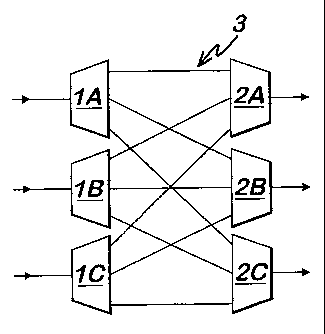
Referring the drawings, Figure 5 shows schematically a simple route-and-select
optical
crossbar switch having three input switches lA, 1B and 1C, three output
switches 2A,
2B and 2C and an optical transpose system (indicated generally by the
reference
numeral 3) sandwiched between the input switches and the output switches. The
optical transpose system may be as described in the specification of our
international
patent application No. PCT/GBO1/03643.
Figure 6 is a schematic representation of a route-and-select optical crossbar
switch
using transmission geometry. This switch includes nine mesolenses 11 arranged
in a
3x3 regular grid, each of which is associated with a respective light source
(not shown).
A respective SLM 12 is associated with each of the mesolenses 11. Each of the
SLMs
12 has nine output beams corresponding to its input beam from the respective
mesolens
11, and the SLMs are programmable to deflect the input beam into the required
output
beam direction. A macrolens 13 rearranges the beams input thereto from the
SLMs 12,
and directs these beams to nine SLMs 14, each of which is associated with a
respective
mesolens 15. Each mesolens 15 is associated with a respective light receiving
device
(not shown). It will be apparent that, by suitable programming of the SLMs 12
and 14,
any light source can be switched to any light receiving device.
Figure 7 is a schematic representation of a route-and-select optical crossbar
switch
using reflective geometry. This switch includes eight input transmitters 21
which are
arranged in a plane P 1,. the transmitters being the form of a regular 3 x 3
grid array with
the middle member missing. The beams (not shown) from the transmitters 21 pass
through a lens 22 in a plane P2 and a lens 23 in a plane P3 to a first
deflector array of
eight SLMs 24. The SLMs 24 are arranged in a plane P4 in a regular 3 x 3 grid
array
with the central member missing. This arrangement could be modified by
omitting any
member of the 3x3 grid.
The SLMs 24 act to reflect incoming beams back through the lens 23 to a second
deflector array constituted eight SLMs 25. The SLMs 25 are arranged in a plane
PS in a
regular 3 x 3 grid with the central member missing. The SLMs 25 reflect
incoming
beams back through the lens 23 and an output lens 26 (in a plane P6) to eight
light
CA 02466672 2004-05-07
WO 03/041421 PCT/GB02/04990
6
receptors 27. The receptors 27 are arranged in a plane P7 in a regular 3 x 3
grid with
the central member missing.
The arrangement is such that the lenses 22 and 23 together image the
transmitters 21 on
to the SLMs 24 of the first deflector array. The lenses 26 and 23 image the
output
plane receptors 27 on to the SLMs 25 of the second deflector array. The lens
23
converts the angular deflection of light beams received from the SLMs 24 into
spatial
shifts of light onto the SLMs 25 of the second deflector array. Thus, each SLM
24
allows light from its associated transmitter 21 to be directed onto any one of
the SLMs
25 of the second deflector array. The SLMs 25 correct the angle of incidence
of the
light from a given transmitter 21 so that it reaches an associated receptor
27.
In practice, the transmitters 21, which may be optical fibres, lasers,
modulators or light
emitting diodes (LEDs) and the receptors 27, which may be optical fibres or
photo
receivers, may be placed respectively slightly in front of the plane of the
transmitters
and behind the plane of the receptors. In this case, microlens arrays (not
shown) could
be placed in the input plane and the output plane in the positions where the
transmitters
21 and 27 are not shown to be, to match the characteristics of the actual
transmitters
and receptors used to the beam parameters within the optical cross connect.
The lenses
22, 23 and 26 perform an optical Fourier transform, and may be constructed as
compound lenses.
It will be apparent that, by suitable programming of the SLMs 24 and 25, any
transmitter 21 can be switched to any receptor 27.
Figure 8 is a schematic representation of the switch of Figure 7 illustrating
how two
incident beams are routed through the switch. For simplicity, the Figure 8
shows only
the lenses 22, 23 and 26, and four of the deflectors 24 and 25. In this
figure, the
deflectors 24 and 25 axe shown as plane mirrors, but it will be appreciated
that, in
practice, they axe SLMs as described above with reference to Figure 7.
CA 02466672 2004-05-07
WO 03/041421 PCT/GB02/04990
7
Considering a light beam incident upon the lens 22 from one of the
transmitters 21 (not
shown in Figure 8) this beam being shown in full lines. The beam passes
through the
lens 22, through the lens 23 and then to the deflector 24a, where it is
reflected back
through the lens 23 and on to the deflector 25a, where it is reflected back to
the lens 23
where it is redirected to the lens 26. The beam is then redirected to an
output plane
receptor 27 (not shown in Figure 8). In a similar manner another beam incident
upon
the lens 22, this being shown in dotted lines, passes to the lens 23, then to
the deflector
24b, then to the lens 23, then to the deflector 25b, then to the lens 23, then
to the lens
26, and finally to an output receptor.
The switch shown in Figure 8 is configured in what is known as a bar state,
and Figure
9 shows the switch configured in what is known as a cross state. Figure 8
shows that a
beam incident at the top of the lens 22 from an upper transmitter is delivered
at the top
of the lens 26 and hence to the top receptor. Figure 9 shows the switch
directing an
incident top beam to a bottom receptor, and vice versa.
Figures 10 to 17 show schematically alternative forms of broadcast-and-select
optical
crossbar switches. Thus, ~ Figure 10 shows a broadcast-and-select crossbar
switch
having a regular grid of sixteen input sources 31, each of which is
constituted by a
regular grid of sixteen individual light sources 32. A respective mesolens 33
is
associated with each of the input sources 31. Localised electrical fan-out of
the light
sources 32 of each input source 31 is provided, as shown schematically by the
reference
numeral 34. The light sources 32 of each input source 31 are electrically
gated, as
indicated, so that only one of these light sources emits a light beam to the
associated
mesolens 33.
The light beams are re-directed by the mesolenses 33 to pass through a
macrolens 35,
where the beams are re-arranged. The beams then pass to a regular grid of
sixteen
mesolenses 36, each of which is associated with a respective output device 37.
The
output devices 37 are arranged in a regular grid of sixteen such devices, each
of which
is associated with a regular grid of sixteen light sinks 38. Localised
electrical fan-in of
the light sinks 38 occurs, as indicated by the reference numeral 39.
CA 02466672 2004-05-07
WO 03/041421 PCT/GB02/04990
8
It will be apparent that, by suitable electrical gating of the light sources
32, any input
source 31 can be directed to any output device 37. In this connection, it
should be
noted that each of the light sources 32 is associated with a respective light
sink 38 of a
respective output device 37. The electrical fan-out and/or fan-in may occur
remotely
from the optical assembly, if optical fibres are used to connect the light
sources 32
and/or the light sinks 38 to the optical assembly. In this case, the light
sources 32 could
be, for example, VCSELs and the light sinks 38 could be, for example,
photodetectors.
The optical crossbar switch shown in Figure 11 is a modification of that shown
in
Figure 10, so like reference numerals will be used for like parts, and only
the
modification will be described in detail. The only modification is that the
electrical
gating occurs at the localised electrical fan-in of the light sinks 38, this
being indicated
by the reference numeral 39. Here again, the electrical fan-out and/or fan-in
may occur
remotely from the optical assembly, if optical fibres are used to connect the
light
sources 32 and/or the light sinks 38 to the optical assembly. In this case,
the light
sources 32 could be, for example, VCSELs and the light sinks 38 could be, for
example, photodetectors.
Similarly, the optical crossbar switch shown in Figure 12 is a modification of
that
shown in Figure 10, so like reference numerals will be used for like parts,
and only the
modification will be described in detail. Thus, this crossbar switch uses
optical
shuttering of the light sources 32, for example, using an SLM 34a. Here again,
the
electrical fan-out and/or fan-in may occur remotely from the optical assembly,
if optical
fibres are used to connect the light sources 32 andlor the light sinks 38 to
the optical
assembly. In this case, the light sources 32 could be, for example, VCSELs and
the
light sinks 38 could be, for example, photodetectors.
The optical crossbar switch shown in Figure 13 is a modification of that shown
in
Figure 11, so like reference numerals will be used for like parts, and only
the
modification will be described in detail. Thus, this crossbar switch uses
optical
shuttering of the light sinks 38 instead of electrical gating at the localised
electrical
CA 02466672 2004-05-07
WO 03/041421 PCT/GB02/04990
9
fan-in of the light sinks. As with the embodiment of Figure 12, the optical
shuttering
may be carried out using, for example, an SLM 39a. Moreover, electrical fan-
out
and/or fan-in may occur remotely from the optical assembly, in a similar
manner to that
described above with reference to any one of Figures 10 to 12.
The optical crossbar switch shown in Figure 14 is also a modification of that
shown in
Figure 10, so like reference numerals will be used for like parts, and only
the
modification will be described in detail. Thus, this switch has only one light
sink 38 for
each output device 37. The switch has localised electrical fan-out of the
light sources
32 of each input source 31; and electrical gating or optical shuttering (using
an SLM
34b) is used at the input. Figure 14 shows both these options, and it will be
appreciated
that only one of these will be used in any given optical switch. Localised fan-
in to the
light sinks 38 is achieved by placing these devices where the optical beams
from the
macrolens 35 would normally cross in front of the mesolenses 36 which are
omitted in
this embodiment. Moreover, as with each of the embodiments or Figures 10 to
13,
electrical fan-out and/or fan-in may occur remotely from the optical assembly.
Fan-in
to fibres without loss is only possible when using multimode fibres. In
essence, this is a
realisation of the architecture of Figure 10 or Figure 12 using optical fan-
in.
The optical switch of Figure 15 is a modification of that Figure 14, so like
reference
numerals will be used for like parts, and only the modification will be
described in
detail. Thus, this switch has only one light source 32 for each input source
31.
Localised optical fan-out of the input sources 31 is effected by using a
multiple beam
splitter (for example a grating) 34c provided downstream of the mesolenses 33.
Electrical gating or optical shuttering (using an SLM 39c) of the light sinks
38 is carried
out. Figure 15 shows both these options, and it will be appreciated that only
one of
these will be used in any given optical switch. In essence, this is a
realisation of the
architecture of Figure 11 or Figure 13 using optical fan-out.
Figure 16 is a schematic representation of a modified form of the switch shown
in
Figure 8, illustrating how two incident beams are routed through the switch.
The
central macrolens 23 of the Figure 8 switch is, here, replaced by a reflective
concave
CA 02466672 2004-05-07
WO 03/041421 PCT/GB02/04990
mirror 28. A macrolens 22/26 to the left of the mirror 28 acts as both an
input lens and
an output lens. For simplicity, Figure 16 shows only the macrolens 22/26, a
pair of
deflectors 24 and the curved mirror 28. Input sources (not shown) and light
sinks (not
shown) are positioned to the left of the input/output lens 22/26, these
devices thus
5 constituting bi-directional ports. Alternatively, two sets of input and
output ports may
be co-located. Figure 16 shows two light beams incident upon the lens 22/26
from
respective light sources. Each of these beams passing through the lens 22/26,
then to
the mirror 28, then to a respective one of the deflectors 24, then to the
mirror, where it
is reflected back to the same deflector. After this, each of the beams passes
again to the
10 mirror 28 where it is reflected back through the lens 22/26, and hence to a
respective
light sink. As with the arrangement of Figure 8, this switch is configured in
what is
known as a bar state.
Figure 17 is a schematic representation of a modified form of the switch shown
in
Figure 9, and is similar to the switch of Figure 16, in that it includes an
input/output
macrolens 22/26, a curved mirror 28 and a pair of deflectors 24. As with the
embodiment of Figure 16, input sources (not shown) and light sinks (not shown)
are
positioned to the left of the input/output lens 22/26, these devices either
being
co-located or constituting bi-directional ports. Here again, Figure 17 shows
the route of
two beams passing through the switch. As with the arrangement of Figure 9, the
switch
is configured in what is known as a cross state.
Figure 18 illustrates schematically the large switch constructed using
multiple stages,
each containing a number of basic switch modules. Thus, this switch includes
four
input sectors 41, each of which has four input ports 42. The input sectors 41
are
connected to four output sectors 43, each of which has four output ports 44,
via eight
4x4 crossbar switches 45. This arrangement permits the number of connections
between any sector pair to be varied between zero and eight paths. If the
input and
output sectors 41 and 43 are also crossbar switches, the result is a 16x16
Clos switch
that is capable of strictly non-blocking interconnection of any input
port/output port
pair. A transpose interconnection appears naturally between the stages of this
switch,
this switch is known as a "sector switch", and is constituted by the central
stage of eight
CA 02466672 2004-05-07
WO 03/041421 PCT/GB02/04990
11
crossbar switches 45 together with the two transpose interconnections between
that
stage and the input and output sectors 41 and 43.
Figure 19 illustrates schematically one of the crossbar switches 45 of Figure
18. This
switch is substantially identical to that of Figure 9 without the first and
third stage
lenses 22 and 26. Thus, this switch 45 has a central macrolens 23 and
deflectors 24 and
25. For simplicity, only two input beams (shown respectively in full and
dotted lines)
are shown, these beams coming from input sectors 41 of the switch assembly
shown in
Figure 18. Similarly, the output beams from the switch 45 pass to output
sectors 43 of
the assembly of Figure 18.
The arrangement of Figure 19 uses reflective deflectors 24 and 25, but the
arrangement
could be modified to use transmissive devices. It would also be possible to
use a
curved mirror such as the mirror 28 of Figure 16 or Figure 17 with the lens 23
removed.
Indeed, any other arrangement capable of accepting angularly-multiplexed beams
at an
input port, re-arranging these beams amongst themselves, and delivering them
in a
angularly-multiplexed form to an output port may be used.
Figure 20 illustrates an optical transpose interconnection between the input
sectors 41
and the array of optical crossbar switches 45 of the switch assembly of Figure
18. This
arrangement is basically the optical transpose system of our International
patent
application number PCT/GBO1/03643 with the first and third stage mesolenses
removed. Thus, a central macrolens 51 performs a transpose interconnection
between
angularly-multiplexed beams, the input beams coming from the input sectors 41,
and
the output beams going to the optical crossbar switches 45 of the assembly of
Figure
18. A similar optical transpose system is provided between the array of
crossbar
switches 45 and the array of output sectors 43.
The arrangement of Figure 20 is a transmission geometry arrangement, but any
other
arrangement capable of performing an optical transpose interconnection between
angularly-multiplexed beams may be used. Moreover, for clarity, not all the
beam
paths are shown in Figure 20.
CA 02466672 2004-05-07
WO 03/041421 PCT/GB02/04990
12
Figure 21 illustrates schematically an implementation of the switch assembly
of Figure
18, having electronic control of the input and output stages. Thus, as shown
in Figure
21, a 4x4 array of input sources 61, each of which is constituted by a regular
4x4 grid of
sixteen light sources 62, is provided. Each of the light sources 62 is
electronically
controlled by means (not shown), and a respective mesolens 63 is associated
with each
input source 61. The mesolenses 63 angularly-multiplex light beams incoming
thereto,
and pass these to a macrolens 64. The macrolens 64 carries out an optical
transpose in
the manner described above with reference to Figure 20. The re-arranged beams
leaving the macrolens 64 then pass to a central crossbar switch array similar
to the
crossbar switches 45 of Figure 18. This array is basically a 4x4 grid of the
optical
switches 45 of Figure 18. The array thus has sixteen mesolenses 65 in a
regular 4x4
grid, with deflectors 66 and 67 on opposite sides thereof.
Figure 21 shows the path of one light beam from a light source 62, this light
beam
passing through a first stage mesolens 63, the macrolens 64, a central stage
mesolens
65, a deflector 66, the same central stage mesolens 65, and a deflector 67.
The beam
then passes back through the same central mesolens 65 and on to a second
macrolens
68, which carries out another optical transpose similar to that of Figure 20.
The
re-arranged light beams leave the second macrolens 68 and pass to a third
stage array of
16 mesolenses 69, where input angularly-coded beams are de-multiplexed into
spatially
separate beams for passage to one of a regular 4x4 grid of output devices 70,
each of
which is constituted by a regular 4x4 grid of light sinks 71.
Figure 21 is, therefore, an example of a re-arrangable non-blocking
transparent optical
sector switch consisting of a sandwich of two 256x256 optical transpose
stages, and a
4x4 array of optical route-and-select switches. Each route-and-select switch
can
re-arrange fifteen off axis angularly-multiplexed beams, and can also provide
one fixed
on-axis path. The sixteen switches each have fifteen ports, each of which can
be
connected to any output sector (subject to the overall interconnection being
one-to-one),
plus one additional port that has a fixed connection to its corresponding
sector by the
fixed central stage paths. Strictly non-blocking operation may be achieved by
CA 02466672 2004-05-07
WO 03/041421 PCT/GB02/04990
13
increasing the number of route-and-select switches in the central stage, and
re-dimensioning the transpose interconnections appropriately.
Figure 22 illustrates schematically an all-optical implementation of the
switch assembly
of Figure 18. The central portion of this embodiment is identical with the
central
portion of the embodiment of Figure 21, so like reference numerals will be
used for like
parts, and only the input and output stages will be described in detail.
Similarly, this
embodiment has input sources 61 constituted by light sources 62, input
mesolenses 63,
output mesolenses 69, output devices 70 and light sinks 71, all of which are
as
described above with reference to Figure 21.
A 4x4 array of crossbar switches similar to the switches 45 of Figure 18 is
positioned
between the first stage mesolenses 63 and the macrolens 64. A similar 4x4
array of
crossbar switches similar to the switches 45 of Figure 18 is arranged between
the
macrolens 68 and the third stage mesolenses 69. Each of these crossbar switch
arrays
has sixteen mesolenses 65 in a regular 4x4 grid, with deflectors 66 and 67 on
opposite
sides thereof.
Figure 22 shows the path of one light beam from a light source 62, this beam
passing
through a first stage mesolens 63, a mesolens 65 of the first stage array of
optical
crossbar switches, and then onto the macrolens 64 via the deflectors 66 and 67
and the
same mesolens 65. Passage of this light beam is then the same as for the
embodiment
of Figure 21, until the beam leaves the macrolens 68, when it passes through a
mesolens 65 of the third stage array of optical crossbar switches, and then
onto a light
sink 71 via the deflectors 66 and 67, the same mesolens 65 and a mesolens 69.
Figure 22 is, therefore, an example of a re-arrangeable non-blocking
transparent optical
Clos switch. In the example shown, 15x15 inputs may be connected in any
permutation
to the same number of outputs. Connections may also be set up between a total
of
16x16 inputs and 16x16 outputs, by making use of the less flexible fixed on-
axis path
through the route-and-select switches. Strictly non-blocking operation may be
achieved
CA 02466672 2004-05-07
WO 03/041421 PCT/GB02/04990
14
by increasing the number of centre stage route-and-select switches, and re-
dimensioning
the transpose interconnection stages appropriately.
Each of the optical crossbar switches described above could be configured as a
fixed
arbitrary interconnection, or as a re-configurable interconnection. In the
former case,
the deflectors would be configured by using a deflection technology that may
be custom
designed, but is otherwise permanent. Computer generated holography (CGH) is a
suitable technology for such deflectors. Masks that define the microstructure
of a CGH
deflector are designed by a computer. There are also low cost manufacturing
methods
that allow the replication of a master CGH deflector, for example by
embossing. A
CGH deflector can contain one or more grating structures that diffract
incident light
into one or more desired directions. CGH deflectors may be made in transparent
materials for use in the transmission geometry configurations, or they may be
made in
reflective materials for use in the reflection geometry co~gurations.
It would also be possible to use other deflection technologies such as micro
mirrors,
prisms and beam splitters. A master deflector might be made using some
flexible
manufacturing process (such as diamond turning), and then replicated, for
example by
embossing. It is also possible to use materials that permanently change
structure in
response to a suitable treatment such as optical exposure.
Where a re-configurable interconnection is required, any electro-optic
technology
capable of forming gratings, prisms or mirrors can be used. In particular,
SLMs can be
used as programmable CGH deflectors, that is to say as variable gratings. SLMs
can be
transmissive or reflective. In the case of liquid crystal based SLMs, a plane
mirror is
placed behind the liquid crystal cell to achieve reflective operation. The
reflective
geometry is the most convenient when using silicon VLSI electronics to address
the
individual pixels of the SLM. A variable reflection grating emulates a re-
orientable
mirror. However, strictly speaking, the physics is different, as gratings rely
on
diffraction and mirrors on reflection.
CA 02466672 2004-05-07
WO 03/041421 PCT/GB02/04990
1S
Liquid crystal devices that act as variable gratings, prisms and even lenses
might be
used in the re-configurable interconnections. The micro electro mechanical
systems
(MEMS) technology could be used to translate microlenses or rotate microprisms
to
effect a deflection, rather than using gimballed micromirrors. Deformable
mirror
technology also exists in which piezo actuators deform a flexible or faceted
mirror. A
"phase only" silicon MEMS SLM, that is essentially a miniature version of the
type of
faceted mirror used in astronomy, may also be used. In this case, a variable
phase
grating would be formed.
It will also be appreciated that beam splitting mirrors (for example
reflective
multiplexed gratings) may constitute the deflectors of any of the embodiments
described above, thereby to implement mufti-casting at the price of fan-out
loss. If
more than one channel is fanned-in to an output that supports fewer transverse
modes
than the number of beams fanned in, there is also a fan-in loss.
It will be apparent that modifications could be made to the optical crossbar
switches
described above. In particular, the use of concave lenses at the input and
output would
result in slightly shorter systems, and the system may be folded to reduce
length, by
using mirrors.
Overall, this system produces the Fourier transform, at the output, of a beam
at the
associated input. Conventional systems would, on the other hand, image.
However, by
suitable choice of lenses, it is possible to arrange that the size and
numerical apertures
of the beams at the input and the output are identical, allowing interfacing
with optical
fibres without loss in principle. In particular, in the case of monomode
beams, a
Gaussian input beam is transformed to a Gaussian output beam. If necessary, an
imaging system can be achieved by displacing the inputs and outputs from the
focal
planes, or by using supplementary optics.
In the reflective configurations, the action of the first deflector
encountered is to route
to a destination, and the action of the second deflector encountered is to
select an input.
CA 02466672 2004-05-07
WO 03/041421 PCT/GB02/04990
16
Advantages of the reflective arrangements are:-
1. There is no optical fan-out/fan-in for a unicast connection, in contrast to
a
broadcast-and-select switch. The system is, therefore, lossless in principle,
even when
working between mono mode fibre inputs and outputs.
2. The deflectors operate in reflection, which permits the use of devices made
on the
surface of plane substrates, for example MEMS mirror arrays, ferroelectric
liquid
crystal over Si VLSI SLMs.
3. A reflective geometry is achieved without the use of beam splitters that
introduce
excessive insertion loss or polarisation sensitivity, if polarisation beam
splitters are
used to avoid insertion loss. The system is, therefore, suitable for use in
optical fibre
communications applications.
4. It is transparent, and there is no restriction to the data rate. ~nly the
reconfiguration time is restricted by the deflection technology used.
5. It is bi-directional, so that the system is compatible with full duplex
operation.
6. It is wavelength independent (when using mirror deflectors) or wavelength
insensitive (when using grating deflectors). The system is, therefore,
compatible with
wavelength division multiplexed (WDM) systems.