Note: Descriptions are shown in the official language in which they were submitted.
CA 02467174 2004-05-14
WO 03/045836 PCT/AU02/00537
-1-
DIFFERENTIAL, STRESS REDUCTION IN THIN FILMS
FIELD OF THE INVENTION
The present invention relates to a method of manufacture of crystalline thin
film
structures having reduced differential stress build up, and to the crystalline
thin film
structures that result from the application of this method.
The invention has been developed primarily for use in the manufacture of micro-
electro mechanical systems (MEMS) formed using CMOS semiconductor chip
technology
to from materials suited to this particular manufacturing process, and will be
described
hereinafter with reference to this preferred application. However, it will be
appreciated by
those skilled in the art, that the invention may be applied to other thin film
structures where
it is similarly desirable to reduce differential stress levels within the thin
film structure.
15 BACKGROUND OF THE INVENTION
Processes for the construction of micro-electro mechanical systems (MEMS) are
characterised by the formation of micro actuator devices and mechanisms in
multi layered
wafer structures. Often these layers comprise thin films of different
materials having
different properties. For example, some of the layers may be required to be
conductive,
20 such as where the mechanism includes a heating element as may be used with
a thermal
bend actuator or the like.
Thin film structures of this kind are typically formed as a wafer using a
molecular
deposition process such as "sputtering" which causes the requisite material to
be deposited
at a molecular level until the desired layer thickness has been attained. With
these
25 deposition processes, the first layer of material typically forms small
seed crystals which
adhere to and align themselves with the supporting substrate. However,
subsequent
deposited material tends to self align on top of these seed crystals and
because of the
restraint placed on the development of the growing crystals by the substrate
and adjacent
crystals, further deposition of the same material tends to thus form columnar
crystals.
3o Unfortunately, the columnar crystals and the underlayer of small seed
crystals have quite
different thermal expansion properties and other physical characteristics.
With many
materials, the growing layer also exhibits progressively expanding crystals
during
CA 02467174 2004-05-14
WO 03/045836 PCT/AU02/00537
-2-
deposition due to the dominant growth of some columnar crystals over others.
As a result,
certain crystal boundaries exist through the entire thickness of the film,
these particular
boundaries not only weaken the overall structure, but also representing
potential locations
for the onset of crack propagation.
As a result of this natural film building process, residual stress is induced
into the
material during wafer cooling. This can have several undesirable effects.
Firstly, the
residual stress gradient maybe sufficient to cause a flap beam actuator formed
by this
process to curl, even though its design is such that it is effectively a
clamped or free beam.
This may necessitate a re-design of the structure to include additional
stiffening elements to
counteract any inclination to curl and as a result is highly likely during
operation to require
additional power to operate the actuator to overcome either the residual
stress or the
additional resistance caused by the need to stiffen the structural design.
A common method of reducing stress in thin films is annealing. however, for
many
crystalline thin films, this requires high temperatures which may be
incompatible with the
device structure or previous processing steps. For example, if a crystalline
thin film is
deposited on an integrated circuit with aluminium wiring, then the temperature
must remain
below the melting point of aluminium, which is too low to anneal many
crystalline
materials typically used in integrated circuits made using CMOS techniques.
It is an object of the invention to provide a method and structure to reduce
the
differential stress formed in thin film structures of this kind so as to
overcome or at least
ameliorate these disadvantages of the prior art, or at least offer a useful
alternative.
SUMMARY OF THE INVENTION
According to a first aspect of the invention there is provided a method of
manufacture
of a crystalline thin film structure from a predominant first crystalline
material, said method
including the steps of:
depositing said predominant first crystalline material as two or more sub-
layers; and
depositing between said first crystalline material sub-layers, a layer of
second
crystalline material, said second material possessing a lattice constant that
is different from
that of the first crystalline material, so as to disrupt columnar crystal
growth in said
underlying first crystalline material and thereby form a composite thin film
structure having
CA 02467174 2004-05-14
WO 03/045836 PCT/AU02/00537
-3-
a differential stress profile that is less than the differential stress
profile of a comparative
film formed solely from said predominant first crystalline material.
While the final total internal stress present in a thin film structure
manufactured in
accordance with the invention may be higher than may be achieved when
annealing can be
used, the differential stress is much reduced and the curl tendency of a
released layer can be
reduced by orders of magnitude.
Preferably, the crystalline thin film structure is a layer of a MEMS structure
and more
preferably an operational or active layer of a MEMS structure.
Desirably, the second material is selected to have appropriately compatible
physical
to properties relevant to the intended application, as well as possessing a
lattice constant that is
different from that of the predominant first layer. Where the relevant
physical properties of
the two materials are similar, such as electrical or thermal conductivity, the
thickness of the
second material layer relative to the first material sub-layers is less
significant. However,
where the differences are more pronounced, it is preferable to have a very
thin intermediate
second material layer so as to minimise the impact of the property difference
between the
two materials on the final composite structure. Naturally, the pairing of the
first and second
materials must enable production of a thin film structure having relevant key
properties or
characteristics that are close to that of the selected predominant first
crystalline material.
Preferred combinations of first and second crystalline materials, particularly
suited for
use in MEMS structures incorporating thermal bend actuators are:
titanium nitride as a predominant first material with intermediate layers of
tantalum
nitride; and
silicon as a predominant first material with intermediate layers of germanium.
The combinations are particularly suitable for MEMS constructions formed on
top of
CMOS circuitry.
BRIEF DESCRIPTION OF THE DRAWINGS
A preferred embodiment of the invention will now be described, by way of
example
only, with reference to the accompanying drawings in which:
Figure 1 shows an enlarged partial cross-section of a thin film formed in
accordance
with the prior art techniques;
CA 02467174 2004-05-14
WO 03/045836 PCT/AU02/00537
-4-
Figure 2 shows a length of the thin film of Figure 1 deforming under the
residual
differential stress;
Figure 3 shows a series of clampedlfree thin film strips formed in accordance
with the
prior art techniques;
Figure 4 shows a partial cross-section through a thin film formed in
accordance with
the present invention;
Figure 5 shows the crystal boundarys between the primary and secondary layers
of the
film shown in Figure 4;
Figure 6 shows a thin film formed in accordance with the present invention
where the
l0 deposition of the primary material has been re-seeded three times; and
Figure 7 shows clamped/free end strips of thin film formed in accordance with
the
present invention.
DESCRIPTION OF PREFERRED AND OTHER EMBODIMENTS
Refernng first to figure 1, there is shown a partial cross-section of a
titanium nitride
layer showing the grain morphology. The layer has been built up from a first
side 1 on a
substrate composed of silicon with a thin silicon nitrate coating (not shown).
As can be
seen, the titanium nitride builds up gradually on the silicon nitrate surface
commencing with
a thin layer 2, of small seed crystals which gradually evolve into larger
columnar crystals
2o shown generally at 3. These columnar crystals tend to become progressively
larger during
deposition due to the dominant growth of some columnar crystals over others.
Thus, certain
crystal boundaries exist through the entire thickness of the titanium nitride
layer. These
particular boundaries weaken the titanium nitride layer and would be the
likely location for
the onset of crack propagation.
The differing thermal conductivity and expansion characteristics of the
different
portions of the titanium nitride layer induce residual stress in the wafer
during cooling. As
shown in Figure 2, this residual stress gradient through the layer thickness
tends to cause
the layer to curl. This can adversely affect the function of MEMS devices
formed from the
wafer. In particular, thermoelastic actuators in the form of clamped/free end
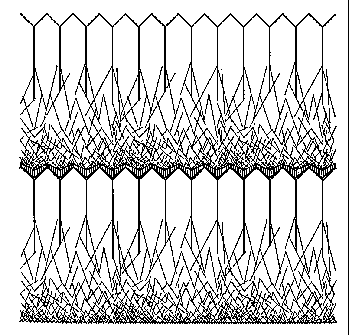
strips are
3o susceptible to a relatively high degree of curl. As shown in Figure 3, a
series of
clamped/free end beam thin titanium nitride strips are shown. The longer and
thinner strips
deflect the most however because of the residual compression on the underside
of the strips
CA 02467174 2004-05-14
WO 03/045836 PCT/AU02/00537
-S
and residual tension on the upper side each strip will tend to curl about it's
longitudinal axis
as well as lateral axis. Wider strips will curl about the longitudinal axis to
produce a deeper
lateral cross-section which gives the strip a greater bending stiffness about
the lateral axis.
A proposed solution for alleviating this differential stress problem, is shown
in
Figures 4 to 7: An extremely thin layer (e.g. 100 Angstroms) of tantalum
nitride is
deposited on top of the titanium nitride at certain levels during the
deposition of the
titanium nitride layer. The tantalum nitride disrupts any predominant titanium
nitride
columnar crystal growth and provides a new re-seeding layer. The tantalum
nitride
effectively acts as a crack inhibitor because the maximum titanium nitride
grain boundary
can only exist between any two tantalum nitride layers.
The presence of the tantalum nitride layers also effectively moderates the
range of
grain sizes present. Thus, the magnitude of any induced stress gradient
related to the grain
size is also moderated. This effectively reduces post fabrication curl.
In this particular preferred embodiment, it is important to note that the
tantalum layer
is thin enough not to affect the mechanical or resistive properties of the
actuator. Tantalum
nitride has a decomposition temperature of 750 degrees Centigrade which is
above that of
titanium nitride.
Examples
A finite element model of a simple beam suitable for use in a thermal bend
actuator
was constructed to investigate residual curl of the tantalum nitride/titanium
nitride layer
structure. The intent of the analysis was to ascertain the relative effect
that different
morphologies have on residual curl rather than the calculation of absolute
values. The
beam model has identical dimensions to the heater section of a centreline
prototype thermal
actuator and was constructed with ten elements through the thickness. A stress
gradient
was indirectly included by applying a linearly varying temperature field
through the entire
thickness. The presence of a tantalum nitride layer is modelled by reapplying
the gradient
from the initial value.
Four different layer combinations were analysed including no tantalum nitride
re-
seeding layer, and one, two and four layers of tantalum nitride. The solutions
resulted in
3o deflections at the beam tip of 0.543, 0.0611, 0.0172 and 0.001 micrometres
respectively. ~ It
should be noted that these values are relative and not absolute.
CA 02467174 2004-05-14
WO 03/045836 PCT/AU02/00537
-6-
The results of the tests show that the inclusion of tantalum nitride layers
can
significantly reduce the amount of post-fabrication curl by progressive orders
of magnitude
depending on the desired overall thickness, number of intermediate layers and
the thickness
of those intermediate layers.
The above described examples relate to a specific conductor layer having
titanium
nitride as the predominant material with intermediate layers of tantalum
nitride. However,
the processes can also be applied to other conductor layer combinations and to
non-
conductor materials such as silicon which can be compared with intermediate
layers of
germanium.
Accordingly, while the invention has been described with reference to only one
use
and two preferred combinations, it will be appreciated by those skilled in the
art that the
invention can be embodied in many other forms.