Note: Descriptions are shown in the official language in which they were submitted.
CA 02467201 2004-05-13
:~~~L?~li:;.lttl?C'~ tit"lil~»f:r t21~i11~'CV) d ~ i1vL11:iCt~j~:
E i~7ures:
h 1~T~S
Unscannable items
recei~jed with this anpLication
(Request original dccuments in File Prep. Szction on tlm 1(~" floor)
DocumeWs i~e:;u a~,~ec ceC;. deLnande ne pouvant titre balal~es
Commander Ies documents ori~inau:c Bans La section de przparation des dossiers
au
IOeme zta?e)
_ ______ . _ _... _. .Lw4 ~u._._.~ae,,roo~~.r~..~.. ..___ _ ..~.~."
..~~:..~..~~M_~~ ~~.m. n,~.~~~ __.__.._._.
CA 02467201 2004-05-13
HIGHLY CONFT17ENTIAL INFORMATION - Page 1 of 13, :;/13/04
SiRiFIC WIRELESS CORP. - dNVENTIONDISCLOSURE' FORM
DATE: May 11 st
TITLE OF INVENTION: Dynamic and Static Spurious correction and control
SUBMITTED BY: Tajinder Manku
ADDRESS:
SiRiFIC Wireless Corporation
460 Phillip Street
Suite 300
Waterloo, Ontario
N2J SJ2
phone - 519-747-2292
fax - 519-747-3996
Please Answer the following questions and attach any
docu.ments/publications/disclosures;
A. Discuss the relevant area or areas of technology.
The area in which this technology fits is in radio technology and in
particular the receiver chain
of a radio. However, it could be extended to those areas in which spurious
issues are generated
by down converting a signal from a carrier to a lower frequency (for example a
cable modem).
The technology is used to move or place spurious components generated by the
radio and an
unwanted RF (Radio Frequency) signal (denote the unwanted l~F signal by a
"blocking signal")
to a frequency location that does not desensitize the wanted RF~ signal.
Desensitization by the
Mocker can occur in varies forms: (i) raising the noise floor, (iii) causing
the overall gain of the
receiver to reduce, or (iii} both (i) and (ii).
B. What problem or problems exist that your invention may solve?
This invention reduces or eliminates blocking signals from desensitizing the
receiver chain.
C. How has this problem, or similar problems, been mitigated in the past?
There are several methods which have been used to mitigate this problem
before. However, in
most of the cases some Mockers do not pass the radio test and are denoted as
exceptions. For a
CA 02467201 2004-05-13
HIGHLY CONFIDENTIAL INFORMATION - Page 2 of 13, 5/13/04
given standard there are a number of exceptions allowed and if you exceed this
amount the radio
will not pass type approval. Below is a listing of the various methods and the
disadvantages/
advantages associated with them:
Super-heterodyne: The super-heterodyne receiver uses a two si:ep frequency
translation method to
convert the signal at RF to a base hand signal. First, the incoming signals
and corruptive noise are
passed through a band pass filter that attenuates out of band signals and
passes the desired signal. At
this stage some of the blocking signals that are out of band are filtered. The
desired signal, plus
residual blocking signals, are amplified and mixed with a first local
oscillator. This causes both a
downconversion and an up conversion in the frequency domain. Usually the
downconverted portion
is retained at the so-called "Intermediate Frequency" (IF). Further faltering
is performed on the signal
at the IF frequency using a discrete device. This filter is a band pass filter
and retains the radio
channel required and further reduces the residual blocking signal. The signal
is then mixed with a
second oscillator that causes frequency translation to base band.
The main problems with super-heterodyne are:
1. The location of the spurious signals is fixed relative to the :EtF wanted
signal in hardware - i.e.
they cannot be changed using a software change.
2. It requires an expensive off chip IF filter
3. The off chip components require design trade-offs that incrc;ase power
consumption and reduce
system gain.
4. Frequency plan is fixed in hardware
Image Rejection Architectures: There are several image rejection architectures
that exist. Among
these, the two most well known are the Hartley Image Rej ection Architecture
and the Weaver Image
Rejection Architecture. Here a spurious signal is created and is located at a
fixed location in
frequency relative to frequency of the wanted signal. This spurious signal is
commonly referred to as
the imagining frequency. The imagining blocking signal is removed using a
combination of phase
shifters and adders that are applied directly to the radio signal itself
or/and the LO signal. Some
methods employ poly-phase filters to cancel the image componf;nts. Generally,
either accurate phase
shifters or accurate generation of a quadrature mixing signal are employed in
these architectures to
cancel the image frequency. The amount of image (or blocker) cancellation is
directly dependent
upon the degree of accuracy in producing the phase shift or in producing the
quadrature mixing
signals. Although the integratability of these architectures is high, them
penfonmance is relatively
poor due to the ~equi~ed accuracy of the phase shifts and quadrature
oscillators. Another
disadvantage here is the location of the Mocker signal (or image frequency) is
fixed relative to the
wanted signal and cannot be moved to another location.
Direct Conversion: Direct conversion architectures performs the RF to base
band frequency
translation in a single step. The RF' signal is mixed with a local oscillator
at the carrier frequency.
There is therefore no image frequency, and no image compe~nents to corrupt the
signal. Direct
conversion receivers offer high integratability, but also have several
important problems. Classical
CA 02467201 2004-05-13
HIGHLY CONFIDENTIAL INFORMATION - Page 3 of 13, 5/13/04
direct conversion receivers have thus far proved useful only for signaling
formats that do not place
appreciable signal energy near DC after conversion to base band. Though direct
conversion does not
suffer from blocking signals in general, there are several typical problems
found in integrated direct
conversion receivers follow:
1. Noise near base band (i.e. 1/f noise) corrupts the desired signal.
Z. Local oscillator leakage creates DC offsets.
3. Local oscillator leakage causes desensitization.
4. Noise inherent to mixed-signal integrated circuits corrupts the desired
signal.
5. Large on-chip capacitors are required to remove unwanted noise and signal
energy near DC.
Near Zero-IF Conversion: This receiver architecture is similar to the direct
conversion architecture,
in that the RF band is brought close to base band in a single step. The
desired signal is not brought
exactly to base-band however, and therefore DC offsets and 1/f noise do not
contaminate the signal.
Image frequencies (i.e. the Mocker) are again a problem as in the super-
heterodyne and image
rejection architectures. Specific problems encountered with these
architectures include:
1. The second down conversion to bring the IF' signal to base-band has to
occur in digital domain
due to spurious issues
2. The relative frequency of the image is fixed based on the. frequency
planning and cannot be
changed.
3. The filters used to filter the IF signal inherently contributes to the
frequency planning, making
them standard specific
4. The need for several balanced signal paths for purposes of image
cancellation.
5. Noise inherent to mixed-signal integrated circuits corrupts the desired
signal.
Harmonic Mixing architectures: This approach uses a number of mixing signals
that are phase
shifted by some desired amount. Irf we assuming x(t) is the incoming RF
signal, and al, az, and a3
are the mixing signals, the output of a harmonic mixing structure equals
x(t)*(al+a2+a3). In this
example, we have assumed three mixing signals. Here, al, a2, and a3 are
constructed so that when
they add they have significant energy at the wanted earner frequency. The
frequency of al, a2, and
a3 are usually the same. In all cases, al+a2+a3 will have other iFrequency
components other than the
wanted carrier frequency. This produces a fixed spurious response. The
disadvantage here is the
spurious are fixed based on the frequency planning of the additive signals
(for example al, a2, and
a3)
VLO technology: VLO technology consists of two mixers coru2ected together. At
the LO ports of
the two mixers (labeled M1 and M2) the signals ~1 and ~2 are applied such that
the overall RF signal
(denoted as x(t)) is multiplied by a signal having significant power at the RF
carrier frequency; that is
y *~z has significant power at the RF frequency. However, in reality there
will be power generated
in places other than the RF earner frequency - denote this power as unwanted
power - this can be
seen in the figure below. This amount of unwanted power is determined by the
timing delay and
CA 02467201 2004-05-13
HIGHLY CONFIDENTIAL INFORMATION - Page 4 of 13, 5/13/01
frequency of signal ~2. The unwanted power will down convert signals located
at the "unwanted
power frequencies". For example, if there is unwanted power at 2104MHz in
~l*c~2 and there is an
out off band blocker signal at 2100MHz, this Mocker will be down converted on
top of the wanted
signal. However, this down converted power will be attenuated by the
difference between "the
power of the wanted" minus "the power of the unwanted" (for the figure below
this is ~37dB) -
denote this amount as WmU (Wanted minus Unwanted). If RFwanted denotes the
wanted P.F
power, the total amount of power at base band is:
BBpower = RFwanted + 10~(-WmU/ 10)'~RFunwanted ( 1 )
There are two ways to fix this problem - (i) adjust the time delay of ~2
thereby modifying the value
of WmU (ii) adjusting the frequency of c~2 such that the RFunwanted tone does
not fall on top of the
wanted signal at base band (iii) select several values of ~2 u.p front by
making sure it does not
produce a problem (these values are stored in memory and be .applied to the
radio chip in a matter
that is related to the RF standard in question). In either approach, the
BBpower is minimized.
Solution (i) does not give significant improvement because of various physical
and circuit
limitations. This patent addresses solutions (ii) and (iii).
x(t) ~-- H PF
~1 c~2
~l (t) J~~ LJ-L. -L
~2 (t) ~.
a ff (t) øl (t) ~ ~2 (t) ~J~~I~I~LI~IJ~ L.~1
unwanted
M1 M2
CA 02467201 2004-05-13
HIGHLY CONFIDENTIAL INFORMATION - Page 5 of 13, 5/13/04
D. What are the advantages of your invention?
There are several advantages to the patent, however the key advantage is the
location of the
spurious profile of ~1*~2 in frequency domain can be modified by adjusting c~z
(which will in turn
modify ~1 accordingly), but the dominate frequency (i.e. with the highest
power) of ~1*~2 equals
the RF frequency and depends of what ~2 is set to. This property is a property
of VLO. No other
radio architecture (to our knowledge) has this fundamental property.
Key Advantages:
1. Spurious profile of ~l*~2 in frequency domain can be modified by adjusting
~2 (which
will in turn modify ~I accordingly), but the dominate frequency (i.e. highest
power tone)
of ~1*~2 equals the RF frequency and is independent of the frequency ~Z is set
to.
2. The spurious profile can change using only software (as in other
architectures the
spurious content is based on the hardware implementation). For example, ~Z can
be
generated via a PLL that can be programmed to generate a range of frequency.
3. using the signal between the two mixers an estimate can be made on the
level of
blocking signal that will in turn determine if ~2 needs adjusting
4. The output of the RX path can be used to determine if a blocker is present
(see
equation (1) by relocating the spurious profile
5. The spurious profile can dynamically change using correction
software/hardware in
combination with the properties in items 2, 3, and 4
6. All the spurious control can be implemented on the radio chip itself
(opposed to the
baseband microprocessing chip)
E. Explain, in detail, preferably with the assistance of drawings or
flowcharts, the best embodiments
or examples of your invention. Include a list of components, if' appropriate.
There are two basic implementations. One consists of dynamically correcting
the spurious
profile so a Mocker will not be placed onto of the desired signal in base
band. The other is
initially selecting a number of ~Z values such that they do not case a
problem. The selection in
this case is based on making sure the RF signal is not corrupted under normal
operation. Any
one skilled in the art of radio would be able to set up some criteria for this
selection from the
teachings herein. The selection could be based on field trials for various ~Z
values or simulation
data.
A. Selecting a number of ~Z values:
For this case the values of ~2 are stored in memory. The memory can be in the
radio, in the
processor, memory on the PCB, or any combination of. Bf;low is a simplified
diagram - see;
CA 02467201 2004-05-13
HIGHLY CONFIDENTIAL INFORMATION - Page 6 of 13, 5/13/04
figure (2). The RF signal (i.e. RFin) contains the wanted signal and any
blocker signal. The
"RX path" is the receiver path and consists of a low noise amplifier, mixers,
base band filters,
and gain elements which are control by in some closed loop manner. The output
of the RX
path consists of two signals (I and Q). These signals can either be analog or
digital signals.
If they are digital signals, an analog to digital element woulLd be absorbed
in the "RX path"
element. The element "VLO generation" generates the signals cal and ~Z from a
"LO" signal
that is controlled via a PLL, and an input from an element i:hat specifies the
frequency of ~Z.
The various frequency values of ~2 are stored in memory. Different frequency
values of ~Z
values may be used for different channels within a standard or for different
standards all
together. The selection of c~Z is based on a system understanding of where
spurious tones can
be placed so that they do not significantly degrade the want;ed RF signal.
Also, ~2 can be
selected so that the least number of exceptions are used. As an example, ~2
can be selected
based on the following criteria:
1. No spurious content is within the band width of the all the channels
2. The first spurious value is >1 OMHz from the edges of the band
RF in RX path
I and Q
signals
~1 f ~2
VLO generator
hid
LO within Phiz 2
PLL loop
n
0
Memory
Phil
Memory could
be in radio or
base band
processor
B. Dynamic Spurious correction
Figure (2)
The dynamic spurious approach is based on making a measurement that indicates
if a blocker
is present, and then adjusting ~G so the Mocker moves to a location that does
not degrade
performance. Below is a simplified diagram - see figure (3). The RF signal
(i.e. RFin)
contents the wanted signal and any blocker signal. The "R:K path" is the
receiver path and
contents a low noise amplifier, mixers, base band filters, artd gain elements
which are
CA 02467201 2004-05-13
HIGHLY CONFIDENTIAL INFORMATION - Page 7 of 13, ,S/13/04
controlled by some closed loop manner. The output of the RX path consists of
two signals (I
and Q). These signals can either be analog or digital signals. If they are
digital signals, an
analog to digital element would be absorbed in the "RX path" element. The
element "VLO
generation" generates the signals ~1 and ~Z from a (i) "LO" signal that is
controlled via a PLL
and (ii) an input from an element that specifies the frequency of c~z. The I
and Q signal is
ported into a detector that determines the power of the signal; this may not
be a true power
detector, but an element that determines the strength of the signal. A timer
is implemented
and determines when the next power measurement should he made after a new ~Z
value is
loaded in. The timer may have information of which RF frame it is looking at,
or when the
next value of ~Z has settled so the next power measurement can be taken. The
two values of
power are compared and the frequency of c~2 is selected based on which ~2
value measures the
minimum amount of power. In general N values of c~z could be compared; where N
is a
number greater than 2 and is an integer.
The element labeled "sense Mocker," is used to sense if a b~locker is present.
The enable and
disable block decides if the correction scheme is enabled based on various
inputs; some may
include if the receiver is enabled, ifthe amplifier gains are set in a
particular condition, and
the registers enable the condition to occur. There may be base-band processor
control for
disabling or enabling the correction scheme directly. The acceptable values of
c~2 are stored
in memory. The acceptable values are determined from a system understanding of
the radio
standard in question.
Additional information on the generation of VLO signals i:9 available in the
following co-
pending patent applications:
a. PCT International Application Serial No. PCT/CA00/00995 Filed September l,
2000,
titled: "Improved Method And Apparatus For Up-Conversion Of Radio Frequency
(RF)
Signals";
b. PCT International Application Serial No. PCT/CA00/00994 Filed September 1,
2000,
titled: "Improved Method And Apparatus For Down-Conversion Of Radio Frequency
(RF) Signals";
c. PCT International Application Serial No. PCT/CA00/00996 Filed September 1,
2000,
titled: "Improved Method And Apparatus For Up-And-Down-Conversion Of Radio
Frequency (RF) Signals"; and
d. PCT International Application Serial No. PCT/CA01/00876 Filed June 19,
2001, titled:
"Improved Method And Apparatus For Up-And-Down-Conversion Of Radio Frequency
(RF) Signals".
CA 02467201 2004-05-13
HIGHLY CONFIDENTIAL INFORMATION - Page 8 of 13, 5/13/04
Memory
Enablel
Sense disable Compare
blodcer
l Power
Signal to Timers detector
sense
blodcer
presense
RF i~ RX path
IandQ
signals
~1 ~2
VLO generator
LO within
J PLL loop
Figure (3)
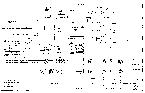
Figure (4) shows an actual implementation of Figure (3). Figure (5) relates
some of the
blocks to those shown in Figure (3). This figure uses three frequency values
of ~2 to
make the comparison on which ~2 minimizes the base-band power. The values of
power
are stored on caps while the next power value is established. The sensing of
the blocker
is done by looking at the power between the two mixers. The power is compared
to some
threshold value. If the power is above this threshold value this would trigger
that a
blocker is present. For the implementation in Figures (4) and (5), the
threshold value is
made programmable. If the amount of power is high compared to the threshold,
and all
the other enabling conditions are correct the correction loop will the
enabled. During this
spurious correction, the gain of the RX path has to be constant. If the gain
changes, the
measurement is corrupted and the loop is reset. One method of holding a
constant gain is
to disable the receiver from reading the any new gain value. The ~2 values are
stored in
the element labeled "MA Storage register". 'The radio in this example is
control via the
processor thru a 3-wire bus and an enabling pin for the receiver (RX enable).
In both
Figure (4) and (5), all the elements in the RX path are :not explicitly shown.
In this
implementation, there is also a 4 bit counter that counts the number of frames
(for
example in GSM). The maximum number of frames that is allowed is 2~4 = 16
frames.
CA 02467201 2004-05-13
HIGHLY CONFIDENTIAL INFORMATION - Page 11 of 13, S/13/04
F. Repeat item E above, for any other important embodiments or examples of
your invention.
In the illustrations (2) to (S), any of the blocks can be partitioned into
other elements of
the wireless device. For example, the power detector element can be placed in
the
baseband processor and does not have to be located in 'the radio device.
The sensing element for a Mocker can be removed completely. In this case, the
loop will
be activated when an enable signal is provided. The enable signal may be
provided by the
base band processor.
It is assumed in (2) to {5) that a known sub-set of ~ZValues are stored in
memory.
However, the values can be selected in any matter that is achif;vable. For
example, if the
frequency of ~Z increases in increments of ~f, ~2 can change by multiplies of
8f. Another
example is ~2 can change in a random or pseudo-random manner.
More aggressive schemes can be implemented to close the dynamic loop faster.
G. Who is/are the inventor(s)? Please provide their name(s), acidress(es) and
citizenship.
Tajinder Manku
263 Lion's Court
Waterloo, ON
N2L 6M7
Canadian Citizen
Masoud Kahrizi
617 Breakwater Cr.
Waterloo, N2K 4H6
Canadian Citizen