Note: Claims are shown in the official language in which they were submitted.
-13-
Claims
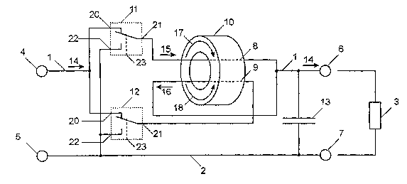
1. A circuit arrangement for the reliable switching
of electrical circuits, in a lead to a current
load (3), comprising a first series path (1, 2),
which electrically connects a first input point
(4, 5) to a first output point (6, 7), and a
second series path (1, 2), which electrically
connects a second input point (4, 5) to a second
output point (6, 7), characterized in that at
least two switching elements (11, 12) are arranged
in parallel with one another in at least one of
the series paths (1, 2), the switching inputs (20)
of said switching elements being connected to the
input point of the series path (4, 5) and the
switching outputs (21) of said switching elements
being connected to the input side of a respective
winding (8, 9) of a transformer (transformer 10),
and the output sides of the windings (8, 9) are
connected to one another and to the output point
of the series path (6, 7), and the windings of the
transformer are embodied such that the magnetic
field strengths (17, 18) of the two component
currents (15, 16) of the load current (14) in the
transformer (transformer 10) act oppositely to one
another, and a capacitance (13) is effective
between the output points (6, 7) of the series
paths (1, 2).
2. The circuit arrangement as claimed in claim 1,
characterized in that a capacitor (19) is arranged
in series with the load in at least one of the
series paths (1, 2).
3. The circuit arrangement as claimed in claim 1 or
2, characterized in that at least one of the
switching elements (11, 12) has a control input
(23) which, when actuated, interrupts the
-19-
connection between the switching input (20) and
the switching output (21).
4. The circuit arrangement as claimed in claim 1 or
2, characterized in that at least one of the
switching elements (11, 12) contains a fuse
located between the switching input (20) and the
switching output (21).
5. The circuit arrangement as claimed in claim 3,
characterized in that at least one of the
switching elements (11, 12) has a further input
(22), which is conductively connected to the
series path (1, 2), and contains at least one
nonlinear element (24) located between the input
(22) and the switching output (21).
6. The circuit arrangement as claimed in claim 5,
characterized in that the nonlinear element (24)
becomes conductive if the polarity of the voltage
at the switching output (21) becomes opposite to
the polarity at the switching input (20).
7. The circuit arrangement as claimed in claim 5,
characterized in that the nonlinear element (24)
becomes conductive if the magnitude of the voltage
at the switching output (21) exceeds the magnitude
of the voltage at the switching input (20).
8. The circuit arrangement as claimed in claim 3,
characterized in that the control inputs (23) of
the switching elements (11, 12) are actuated
virtually simultaneously by a suitable device.
9. The circuit arrangement as claimed in claim 8,
characterized in that the control inputs (23) of
the switching elements (11, 12) are connected to
-15-
one another and are actuated virtually
simultaneously by at least one suitable device.
10. The circuit arrangement as claimed in claim 1 or
2, characterized in that at least one of the
switching elements (11, 12) has a control input
(23) which, when actuated interrupts the
connection between the switching input (20) and
switching output (21), and establishes the
connection to a further switching input (22),
which is conductively connected to the series path
(1, 2).
11. The circuit arrangement as claimed in claim 10,
characterized in that the control inputs (23) of
the switching elements (11, 12) are connected to
one another and are actuated virtually
simultaneously by at least one suitable device.
12. The circuit arrangement as claimed in claim 1 or
2, characterized in that at least one of the
switching elements (11, 12) contains a
controllable component (25, 29) with a control
input (26, 30), which can establish and interrupt
the connection between the switching input (20)
and the switching output (21) of the switching
elements.
13. The circuit arrangement as claimed in claim 1 or
2, characterized in that at least one of the
switching elements (11, 12) contains a
controllable component (27, 31) with a control
input (28, 32), which can establish and interrupt
the connection between the switching input (22)
and the switching output (21) of the switching
elements.
-16-
14. The circuit arrangement as claimed in claim 1 or
2, characterized in that at least one of the
switching elements (11, 12) contains two
controllable components (25, 27) and (29, 31) each
with a control input (26, 28) and (30, 32),
respectively, which can establish and interrupt
the connection between the switching inputs (20)
and the switching outputs (21) and also between
the switching inputs (22) and the switching
outputs (21).
15. The circuit arrangement as claimed in claim 12, 13
or 14, characterized in that the controllable
component comprises at least one relay contact.
16. The circuit arrangement as claimed in claim 12, 13
or 14, characterized in that the controllable
component comprises at least one transistor.
17. The circuit arrangement as claimed in claim 12, 13
or 14, characterized in that the controllable
component comprises at least one thyristor.
18. The circuit arrangement as claimed in claim 14,
characterized in that the control inputs
(26, 28, 30, 32) of the components
(25, 27, 29, 31) are led to a control device (33),
which can assume at least two states, state 1 and
state 2, and which has at least one control input
(36).
19. The circuit arrangement as claimed in claim 18,
characterized in that the control device (33) in
state 1 drives the components (25, 29) such that
the latter conductively connect the switching
inputs (20) to the switching outputs (21) of the
switching elements (11, 12), and drives the
components (27, 31) such that the latter interrupt
-17-
the connection between the switching inputs (22)
and the switching outputs (21) of the switching
elements (11, 12).
20. The circuit arrangement as claimed in claim 18,
characterized in that the control device (33) in
state 2 drives the components (25, 29) such that
the latter interrupt the connections between the
switching inputs (20) and the switching outputs
(21) of the switching elements (11, 12), and
drives the components (27, 31) such that the
latter establish the conductive connection between
the switching inputs (22) and the switching
outputs (21) of the switching elements (11, 12).
21. The circuit arrangement as claimed in claims 18 to
20, characterized in that the control device (33)
is changed over from state 1 to state 2 via the
control input (36), and the control device (33),
upon this state transition, drives the components
(25, 29) virtually simultaneously such that the
connection between the switching inputs (20) and
the switching outputs (21) is interrupted,
subsequently drives one of the components (27) or
(31) such that the connection between the
switching input (22) and switching output (21)
thereof is established, and then drives the second
component (27) or (31) via the control input (28)
or (32) thereof such that the connection between
the switching input (22) and switching output (21)
thereof becomes conductive if the voltage between
the switching input (22) and switching output (21)
thereof has become virtually zero.
22. The circuit arrangement as claimed in claims 18 to
20, characterized in that the control device (33)
is changed over from state 2 to state 1 via the
control input (36), and, upon this state
-18-
transition, drives the components (27, 31)
virtually simultaneously such that the connection
between the switching inputs (22) and the
switching outputs (21) is interrupted,
subsequently drives one of the components (25) or
(29) such that the connection between the
switching input (20) and switching output (21)
thereof is established, and then drives the second
component (25) or (29) via the control input (26)
or (30) thereof such that the connection between
the switching input (20) and switching output (21)
thereof becomes conductive if the voltage between
the switching input (20) and switching output (21)
thereof has become virtually zero.
23. The circuit arrangement as claimed in claims 18 to
20, characterized in that the control device (33)
is changed over from state 1 to state 2 via the
control input (36), and, upon this state
transition, drives the components (25, 29)
virtually simultaneously such that the connection
between the switching inputs (20) and the
switching outputs (21) is interrupted,
subsequently then drives one of the components
(27) or (31) such that the connection between the
switching input (22) and switching output (21)
thereof is established if the voltage between
switching input (22) and switching output (21) has
become virtually zero, and then drives the second
component (27) or (31) via the control input (28)
or (32) thereof such that the connection between
the switching input (22) and switching output (21)
thereof becomes conductive if the voltage between
the switching input (22) and switching output (21)
thereof has become virtually zero.
24. The circuit arrangement as claimed in claims 18 to
20, characterized in that the control device (33)
-19-
is changed over from state 2 to state 1 via the
control input (36), and, upon this state
transition, drives the components (27, 31)
virtually simultaneously such that the connection
between the switching inputs (22) and the
switching outputs (21) is interrupted,
subsequently then drives one of the components
(25) or (29) such that the connection between the
switching input (20) and switching output (21)
thereof is established if the voltage between
switching input (20) and switching output (21) has
become virtually zero, and then drives the second
component (25) or (29) via the control input (26)
or (30) thereof such that the connection between
the switching input (20) and switching output (21)
thereof becomes conductive if the voltage between
the switching input (20) and switching output (21)
thereof has become virtually zero.
25. The circuit arrangement as claimed in claims 18 to
20, characterized in that a voltage source having
alternating polarity, such as, for example, a
mains voltage, the secondary winding of a
transformer, the secondary winding of a switched-
mode power supply transformer, is connected to the
input points (4, 5).
26. The circuit arrangement as claimed in claim 25,
characterized in that the control device (33) has
a further control input (34) connected to the
series path (1).
27. The circuit arrangement as claimed in claim 25,
characterized in that the control device (33) has
a further control input (35) connected to the
series path (2).
-20-
28. The circuit arrangement as claimed in claims 21 to
27, characterized in that the transition from
state 2 to state 1 in the switching device (33) is
triggered by the control input (34) or (35) when
the voltage between input point (4) and input
point (5) becomes positive, and the transition
from state 1 to state 2 is triggered by the
control input (36).
29. The circuit arrangement as claimed in claims 21 to
27, characterized in that the transition from
state 2 to state 1 in the switching device (33) is
triggered by the control input (39) or (35) when
the voltage between input point (4) and input
point (5) becomes negative, and the transition
from state 1 to state 2 is triggered by the
control input (36).
30. The circuit arrangement as claimed in claims 25 to
27, characterized in that a second voltage source
having alternating polarity, such as, for example,
a mains voltage, the secondary winding of a
transformer, or the secondary winding of a
switched-mode power supply transformer, is
connected to input point (5) and to a further
input point (40) such that the input point (40)
has the opposite polarity to the input point (4).
31. The circuit arrangement as claimed in claim 30,
characterized in that the switching elements
(11, 12) in each case have a further switching
input (41), which is connected to the input point
(40) via a further series path (42), and in each
case have at least one further controllable
component (43, 49) with the control inputs
(45, 46), which controllable component can be
driven such that it establishes a conductive
-21-
connection between switching input (41) and
switching output (21).
32. The circuit arrangement as claimed in claim 31,
characterized in that the control device (33) is
connected to the control input (45) of the
component (43) via a further control output (47),
to the control input (46) of the component (44)
via a further control output (48) and to the
series path (42) via a further input (49).
33. The circuit arrangement as claimed in claim 32,
characterized in that the control device (33),
during the rise of the input voltage (9, 5),
drives the components (25, 27, 29, 31) such that
the switching inputs (20) are conductively
connected to the switching outputs (21) and the
conductive connection between the switching inputs
(22) and the switching outputs (21) is
interrupted, and, during the rise of the input
voltage (40,5), drives the components (27, 31, 43,
94) such that the switching inputs (41) are
conductively connected to the switching outputs
(21), and the conductive connection between the
switching inputs (22) and the switching outputs
(21) is interrupted, and, by means of a suitable
signal of the control input (36) of the control
device (33); the components (25, 29, 43, 44) are
driven such that the conductive connections
between switching inputs (20, 41) and the
switching output (21) are interrupted, and the
components (27, 31) are driven such that a
conductive connection is produced between the
switching inputs (22) and switching outputs (21).
34. The circuit arrangement as claimed in claim 32,
characterized in that the control device (33),
during the fall of the input voltage (4, 5),
-22-
drives the components (25, 27, 29, 31) such that
the switching inputs (20) are conductively
connected to the switching outputs (21) and the
conductive connection between the switching inputs
(22) and the switching outputs (21) is
interrupted, and, during the fall of the input
voltage (40, 5), drives the components (27, 31,
43, 44) such that the switching inputs (41) are
conductively connected to the switching outputs
(21), and the conductive connection between the
switching inputs (22) and the switching outputs
(21) is interrupted, and, by means of a suitable
signal of the control input (36) of the control
device (33), the components (25, 29, 93, 44) are
driven such that the conductive connections
between switching inputs (20, 41) and the
switching output (21) are interrupted, and the
components (27, 31) are driven such that a
conductive connection is produced between the
switching inputs (22) and switching outputs (21).
35. The circuit arrangement as claimed in claim 32,
characterized in that the control device (33),
during the rise of the input voltage (4, 5),
drives the components (25, 27, 29, 31) such that
the switching inputs (20) are conductively
connected to the switching outputs (21) when the
voltage measured at them is virtually zero, and
the conductive connection between the switching
inputs (22) and the switching outputs (21) is
interrupted, and, during the rise of the input
voltage (40, 5), drives the components (27, 31,
43, 44) such that the switching inputs (41) are
conductively connected to the switching outputs
(21) when the voltage measured at them is
virtually zero, and the conductive connection
between the switching inputs (22) and the
switching outputs (21) is interrupted, and, by
-23-
means of a suitable signal at the control input
(36) of the control device (33), the components
(25, 29, 93, 49) are driven such that the
conductive connections between switching inputs
(2041) and the switching output (21) are
interrupted, and the components (27, 31) are then
driven such that a conductive connection is
produced between the switching inputs (22) and
switching outputs (21) if the voltage measured at
them is virtually zero.
36. The circuit arrangement as claimed in claim 32,
characterized in that the control device (33),
during the fall of the input voltage (4, 5),
drives the components (25, 27, 29, 31) such that
the switching inputs (20) are conductively
connected to the switching outputs (21) when the
voltage at them is virtually zero, and the
conductive connection between the switching inputs
(22) and the switching outputs (21) is
interrupted, and, during the fall of the input
voltage (40, 5), drives the components
(27, 31, 43, 44) such that the switching inputs
(41) are conductively connected to the switching
outputs (21) when the voltage at them is virtually
zero, and the conductive connection between the
switching inputs (22) and the switching outputs
(21) is interrupted, and, by means of a suitable
signal at the control input (36) of the control
device (33), the components (25, 29, 43, 44) are
driven such that the conductive connections
between switching inputs (20, 41) and the
switching output (21) are interrupted, and the
components (27, 31) are then driven such that a
conductive connection is produced between the
switching inputs (22) and switching outputs (21)
if the voltage measured at them is virtually zero.
-29-
37. The circuit arrangement as claimed in claims 18 to
20, characterized in that there is connected
between input point (4) and a further input point
(50) a voltage source having alternating polarity,
such as, for example, the secondary winding of a
transformer, which has an additional tapping for
voltage division, such as, for example, a center
tap of the secondary winding of the transformer,
and said additional tapping is connected to the
input point (5) of the circuit arrangement as
claimed in the invention.
38. The circuit arrangement as claimed in claims 25,
26 and 37, characterized in that the input point
(50) is connected by a further series path (51) to
the switching inputs (22) of the switching
elements (11, 12) and to the input (35) of the
control device (33).
39. The circuit arrangement as claimed in claim 38,
characterized in that the control device (33), by
means of a suitable signal at its control input
(36), is switched to state 1 during the first
half-cycle of the input voltage at the input
points (4, 50) and to state 2 during the second
half-cycle of the input voltage, and the
respectively existing state 1 or 2 is maintained
during the zero crossing of the input voltage.
40. The circuit arrangement as claimed in claims 19
and 20, characterized in that the control device
(33), upon the transition from state 2 to state 1,
then drives the components (25, 29) such that they
establish a conductive connection between
switching input (20) and switching output (21) if
the voltage between switching input (20) and
switching output (21) has become virtually zero.
-25-
91. The circuit arrangement as claimed in claims 19
and 20, characterized in that the control device
(33), upon the transition from state 1 to state 2,
then drives the components (27, 31) such that they
establish a conductive connection between
switching input (22) and switching output (21) if
the voltage between switching input (22) and
switching output (21) has become virtually zero.
42. The circuit arrangement as claimed in claims 18,
32 and 38, characterized in that the control
device (33) is embodied as an integrated circuit.
43. The circuit arrangement as claimed in claims 18,
32 and 38, characterized in that the control
device (33) is embodied as an electronic assembly.
44. The circuit arrangement as claimed in claims 18,
32 and 38, characterized in that the control
device (33) is embodied as a potted module.
45. The circuit arrangement as claimed in claims 18,
31, 32 and 38, characterized in that the control
device (33) together with the controllable
components (25, 27, 29, 31, 43, 44) is embodied as
an integrated circuit.
46. The circuit arrangement as claimed in claims 18,
31, 32 and 38, characterized in that the control
device (33) together with the controllable
components (25, 27, 29, 31, 43, 44) is embodied as
an electronic assembly, hybrid circuit, thick-film
circuit or thin-film circuit.
47. The circuit arrangement as claimed in claims 18,
31, 32 and 38, characterized in that the control
device (33) together with the controllable
components (25, 27, 29, 31, 43, 44) is embodied as
-26-
a potted module or module encapsulated by a
housing.
48. The circuit arrangement as claimed in claim 1,
characterized in that the two windings (8, 9) of
the transformer (10) are embodied as two parallel-
routed lines or conductor tracks of a printed
circuit, which are connected to the switching
elements (11, 12) and the output point (6) of the
circuit arrangement as claimed in the invention
such that the component currents (15, 16) of the
load current (14) flow through them in an opposite
direction.
49. The circuit arrangement as claimed in claim 1,
characterized in that the capacitance (13) is
formed from two parallel-routed lines or conductor
tracks of a printed circuit.