Note: Descriptions are shown in the official language in which they were submitted.
CA 02467693 2008-05-06
, =
52867-7
Superconductor Cables and Coils
TECHNICAL FIELD
The invention relates to superconductor cables and
magnetic devices.
BACKGROUND
Multi-layer superconductor articles, such as
tapes, having various architectures have been developed.
Such articles often include a substrate and a superconductor
layer. Typically, one or more buffer layers are disposed
between the substrate and the superconductor layer.
SUbIlMARY
In general, the invention relates to
superconductor cables and magnetic devices.
According to the present invention, there is
provided an article comprising: a first layer comprising a
first superconductor material; a second layer comprising a
first electrically conductive material, the second layer
being mechanically coupled to the first layer so that, when
bent, the first and second layers have a first neutral
mechanical axis; a third layer comprising a second
superconductor material; and a fourth layer comprising a
second electrically conductive material mechanically coupled
to the third layer, so that, when bent, the third and fourth
layers have a second neutral mechanical axis different than
the first neutral mechanical axis, wherein the second and
fourth layers are in electrical communication.
In one aspect, the invention features an article
that includes a first layer formed of a first superconductor
material and a second layer formed of a first electrically
1
CA 02467693 2007-05-03
52867-7
conductive material. The article also includes a third
layer formed of a second superconductor material and a
fourth layer formed of a second electrically conductive
material. The second layer is mechanically coupled to the
first layer (e.g., mechanically coupled at points other than
their ends), and the fourth layer is mechanically coupled to
the third layer (e.g., mechanically coupled at points other
than their ends). The second and fourth layers are in
electrical communication. The first and second layers have
a neutral mechanical axis when bent that is different than
the neutral mechanical axis of the third and fourth layers
when bent.
The phrase "mechanically coupled", as used herein,
refers to a force between (e.g., at the interface of) two
layers that substantially reduces (e.g., eliminates) the
ability of one layer to move independently of the other
layer. One example of mechanically coupled layers is two
layers that are chemically bonded together. Another example
of mechanically coupled layer is two layers that are
metallurgically bonded together. An additional example of
mechanically coupled layers is two layers that are each
adhered to an adhesive layer therebetween. It is to be
noted that two layers (or other articles, such as tapes)
generally are not mechanically coupled when the layers (or
articles) are held in compression against each other by a
force acting from outside (as opposed to at the interface
of) the two layers. For example, if two tapes are
la
CA 02467693 2004-05-17
WO 03/047006 PCT/US02/33455
wrapped within insulation that provides a compressive force that holds the
tapes in
proximity to each other, this force itself does not render the tapes
mechanically
coupled, although the tapes may otherwise be mechanically coupled (e.g., if
the tapes
are chemically or metallurgically bonded to each other).
The article can be configured so that the second and fourth layers can move
independently of each other.
The first and second superconductor materials can be the same or different.
For
example, one or both of the superconductor materials can be a rare earth
superconductor material, such as YBCO.
The first and second electrically conductive materials can be the same or
different. For example, the first and second electrically conductive materials
can be a
metal (e.g., copper) or an alloy (e.g., a copper alloy).
The first and second layers can be in the form of a tape. The second and third
layers can be in the form of a tape.
The article can further include first and second substrates. The first layer
can be
between the first substrate and the second layer, and the third layer can be
between the
second substrate and the fourth layer.
The article can further include first and second buffer layers. The first
buffer
layer can be between the first substrate and the first layer, and the second
buffer layer
can be between the second substrate and the third layer.
In some embodiments, the first substrate layer has a thickness that is about
equal to a combined thickness of the first layer, the first buffer layer, and
the second
layer.
In certain embodiments, the fourth layer has a thickness that is about equal
to a
combined thickness of the third layer, the second buffer layer, and the second
substrate
layer.
The article can further include first and second cap layers. The first cap
layer
can be between the first and second layers, and the second cap layer can be
between the
third and fourth layers.
The article can further include an interfacial layer between the second and
fourth layers. The interfacial layer is generally formed of an electrically
conductive
material and can be, for example, capable of reducing oxidation of the second
and
2
CA 02467693 2007-05-03
52867-7
fourth layers, and/or reducing friction between the second
and the fourth layer. In some embodiments, the interfacial
layer is at least partially formed of graphite.
Also according to the present invention, there is
provided an article comprising: a first helically wound
superconductor tape that includes a superconductor layer and
an electrically conductive layer, the first helically wound
superconductor tape having a first neutral mechanical axis
when bent; and a second helically wound superconductor tape
that includes a superconductor layer and an electrically
conductive layer, the second helically wound superconductor
tape having a second neutral mechanical axis when bent, the
second neutral mechanical axis being different than the
first neutral mechanical axis, wherein the electrically
conductive layers of the first and second superconductor
tapes are in electrical communication.
In another aspect, the invention features an
article (e.g., a cable) that includes first and second
helically wound superconductor tapes. The first tape
includes a superconductor layer and an electrically
conductive layer, and the second tape that includes a
superconductor layer and an electrically conductive layer.
The electrically conductive layers of the first and second
tapes are in electrical communication (e.g., in electrical
communication at more than one position, such as by
contacting each other in more than one location). The first
helically wound superconductor tape has a neutral mechanical
axis, and the second helically wound superconductor tape has
a different neutral mechanical axis.
The first and second helically wound tapes can be
configured so that they can move independently of each
other.
3
CA 02467693 2007-05-03
52867-7
The article can further include a forming element
around which the first and second tapes are helically wound.
In some embodiments, the superconductor layers of
the first and/or second superconductor tapes are
mechanically compressed.
The first and second helically wound
superconductor tapes can have a common helical axis.
In some embodiments, the article further includes
third and fourth helically wound superconductor tapes. The
third helically wound superconductor tape includes a
superconductor layer and an electrically conductive layer,
and the fourth helically wound superconductor tape includes
a superconductor layer and an electrically conductive layer.
The electrically conductive layers of the third and fourth
superconductor tapes have more than one point of electrical
communication (e.g., by contacting each other in more than
one location). The third and fourth helically wound
superconductor tapes can have a common helical axis.
In certain embodiments, the electrically
conductive layers of the first and second superconductor
tapes at least partially overlap. In some embodiments, the
electrically conductive layers of the first and second
superconductor tapes substantially entirely overlap.
According to the present invention, there is
further provided an article, comprising: a first plurality
of helically wound superconductor tapes, each tape in the
first plurality of helically wound superconductor tapes
including a layer of a superconductor material and a layer
of an electrically conductive material, each tape in the
first plurality of helically wound superconductor tapes
4
CA 02467693 2007-05-03
52867-7
being wound in parallel in a first direction; and a second
plurality of helically wound superconductor tapes, each tape
in the second plurality of helically wound superconductor
tapes including a layer of a superconductor material and a
layer of an electrically conductive material, each tape in
the second plurality of helically wound superconductor tapes
being wound in parallel in a second direction opposite the
first direction, wherein the layer of the electrically
conductive materials in each tape in the first plurality of
tapes has more than one position of electrical communication
with the layer of electrically conductive material in each
tape of the second plurality of tapes.
In a further aspect, the invention features an
article that includes first and second pluralities of
helically wound tapes. In the first plurality of helically
wound superconductor tapes, each tape includes a layer of a
superconductor material and a layer of an electrically
conductive material, and each tape is wound in parallel in a
first direction. In the second plurality of helically wound
superconductor tapes, each tape includes a layer of a
superconductor material and a layer of an electrically
conductive material, and each tape is wound in parallel in a
second direction opposite the first direction. The layer of
the electrically conductive materials in each tape in the
first plurality of tapes has more than one position of
electrical communication with the layer of electrically
conductive material in each tape of the second plurality of
tapes (e.g., by contacting each other in more than one
location).
In some embodiments, the first and second
pluralities of helically wound superconductor tapes have a
common helical axis.
4a
CA 02467693 2007-05-03
52867-7
In certain embodiments, the electrically
conductive layers of each tape in the first plurality of
superconductor tapes at least partially overlap with the
electrically conductive layers of each tape in the second
plurality of superconductor tapes.
Each of the tapes in the article can have a
different neutral mechanical axis when bent than the neutral
mechanical axis of any of the other tapes when bent.
According to the present invention, there is
further provided a superconducting magnetic coil,
comprising: a first coiled superconductor tape coiled about
a coil axis, the first coiled superconductor tape
comprising: a superconductor layer; and an electrically
conductive layer having a surface forming an inner surface
of the first coiled superconductor tape, the inner surface
of the first coiled superconductor tape facing the coil axis
of the first coiled superconductor tape; and a second coiled
superconductor tape coiled about a coil axis, the second
coiled superconductor tape, comprising: a superconductor
layer; and an electrically conductive layer having a surface
that forms an outer surface of the second coiled
superconductor tape, the outer surface of the second coiled
superconductor tape facing away from the coil axis of the
second coiled superconductor tape, wherein the first and
second coiled superconductor tapes are configured so that
inner surface of the first superconductor tape is adjacent
the outer surface of the second superconductor tape.
In an additional aspect, the invention features a
superconducting magnetic coil that includes first and second
coiled superconductor tapes. Each coiled superconductor
tape is coiled about a respective coil axis. The first
coiled superconductor tape includes a superconductor layer
4b
CA 02467693 2007-05-03
52867-7
and an electrically conductive layer. The electrically
conductive layer of the first coiled superconductor tape has
a surface that forms an inner surface of the first coiled
superconductor tape. The inner surface of the first coiled
superconductor tape faces the coil axis of the first coiled
superconductor tape. The second coiled superconductor
includes a superconductor layer and an electrically
conductive layer. The electrically conductive layer of the
second coiled superconductor tape has a surface that forms
an outer surface of the second coiled superconductor tape.
The outer surface of the second coiled superconductor tape
faces away from the coil axis of the second coiled
superconductor tape. The first and second coiled
superconductor tapes are configured so that inner surface of
the first superconductor tape is adjacent the outer surface
of the second superconductor tape.
The first and second superconductor tapes in the
magnetic coil can have different neutral mechanical axes
from each other.
4c
CA 02467693 2004-05-17
WO 03/047006 PCT/US02/33455
In some embodiments, the first and second coiled superconductor tapes contact
each other.
In certain embodiments, the first and second coiled superconductor tapes are
wound together.
In some embodiments, the coil axis of the first superconductor tape is the
same
as the coil axis of the second superconductor tape.
In certain embodiments, the first and second superconductor tapes are coiled
about each other.
In some embodiments, the superconductor layer and electrically conductive
layer of the first superconductor tape are mechanically coupled (e.g.,
mechanically
coupled at points other than their ends), and the superconductor layer and
electrically
conductive layer of the second superconductor tape are mechanically coupled
(e.g.,
mechanically coupled at points other than their ends).
In certain embodiments, the superconductor layers of the first andlor second
superconductor tapes are mechanically compressed.
The superconducting magnetic coil can further include an interfacial layer
disposed between the adjacent first and second superconductor tapes.
The superconducting magnetic coil can further include third and fourth coiled
superconductor tapes. Each of the third and fourth coiled superconductor tapes
is
coiled about a respective coil axis. The third coiled superconductor tape
includes a
superconductor layer and an electrically conductive layer. The electrically
conductive
layer of the third coiled superconductor tape has a surface that forms an
inner surface of
the third coiled superconductor tape. The inner surface of the third coiled
superconductor tape faces the coil axis of the third coiled superconductor
tape. The
fourth coiled superconductor includes a superconductor layer and an
electrically
conductive layer. The electrically conductive layer of the fourth coiled
superconductor
tape has a surface that forms an outer surface of the fourth coiled
superconductor tape.
The outer surface of the fourth coiled superconductor tape faces away from the
coil axis
of the fourth coiled superconductor tape. The third and fourth coiled
superconductor
tapes are configured so that inner surface of the third superconductor tape is
adjacent
the outer surface of the fourth superconductor tape.
The architecture of the superconductor articles (e.g., tapes, cables and/or
magnetic coils) can allow multiple superconductor layers to simultaneously be
5
CA 02467693 2004-05-17
WO 03/047006 PCT/US02/33455
compressed (e.g., by being at or below the neutral mechanical axis) when the
articles
are bent.
The architecture of the superconductor articles (e.g., tapes, cables and/or
magnetic coils) can reduce the risk of reduced current density due to, for
example, the
presence of defects (e.g., localized defects, such as a crack a grain
boundary, or the
like) in one or more of the superconductor layers.
The architecture of the superconductor articles (e.g., tapes, cables and/or
magnetic coils) can result in current sharing through, for example, redundant
conducting paths, lower hysteretic losses under alternating current
conditions, enhanced
electrical stability, and/or enhanced thermal stability.
The architecture of the superconductor articles (e.g., tapes, cables and/or
magnetic coils) can result in a favorable stress profile and/or improved
mechanical
properties.
The architecture of the superconductor articles (e.g., tapes, cables, and/or
magnetic coils) can provide improved mechanical stability, improved electrical
stability, enhanced current carrying capacity, and/or favorable economy of
manufacture.
The architecture of the superconductor articles (e.g., tapes, cables and/or
magnetic coils) can reduce mechanical degradation of the operational
superconductor
layer(s) during bending.
The architecture of the superconductor articles (e.g., tapes, cables and/or
magnetic coils) can make it relatively easy to splice the articles.
The architecture of the superconductor articles (e.g., tapes, cables and/or
magnetic coils) can make it relatively easy to achieve termination of tape
stack ups
and/or conductor elements.
The architecture of the superconductor articles (e.g., tapes, cables and/or
magnetic coils) can reduce heating due to, for example, localized defects in
the
superconductor material.
The superconductor articles (e.g., tapes, cables and/or magnetic coils) can be
used in a variety of applications, including, for example, electrical,
magnetic, electro-
optic, dielectric, thermal, mechanical, and/or environmental (e.g.,
protective)
applications.
6
CA 02467693 2004-05-17
WO 03/047006 PCT/US02/33455
Other features, objects, and advantages of the invention will be apparent from
the description and drawings, and from the claims.
DESCRIPTION OF DRAWINGS
Fig. 1 is a cross-sectional view of an embodiment of a superconductor article
including two superconductor tapes;
Fig. 2 is a cross-sectional view of an embodiment of the superconductor
article
of Fig. 1 when bent;
Fig. 3 is a plan view of an embodiment of a superconductor tape;
Fig. 4 is a cross-sectional view of the superconductor tape of Fig. 3;
Fig. 5A is a plan view of an embodiment of a superconductor tape;
Fig. 5B is a plan view of an embodiment of a superconductor tape;
Fig. 6 is a cross-sectional view of an embodiment of a superconductor tape;
and
Figs. 7A and 7B are perspective and plan views, respectively, of an embodiment
of a superconductor magnetic coil.
Like reference symbols in the various drawings indicate like elements.
DETAILED DESCRIPTION
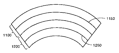
Fig. 1 shows a cross-sectional view of an embodiment of a superconductor
article 1000 that includes multi-layer superconductor tapes 1100 and 1200.
Tape 1100
includes a substrate 1110, a buffer layer 1120, a superconductor layer 1130,
and an
electrically conducting stabilizer layer 1140. Similarly, tape 1200 includes a
substrate
1210, a buffer layer 1220, a superconductor layer 1230, and an electrically
conducting
stabilizer layer 1240. The layers within tapes 1100 and 1200 are mechanically
coupled
(e.g., chemically bonded or metallurgically bonded) to their corresponding
neighboring
layers (e.g., mechanically coupled at points other than their ends), but tapes
1100 and
1200 are configured so that they can move independently of each other because,
while
stabilizer layers 1140 and 1240 contact each other and are in electrical
communication,
surface 440 of stabilizer layer 1140 is not mechanically coupled (e.g., is not
chemically
bonded or metallurgically bonded) to surface 470 of stabilizer layer 1240.
With the architecture of article 1000, electrical current can readily
propagate
3o along and between tapes 1100 and 1200, even if a localized defect is
present in
superconductor layers 1130 and/or 1230. For example, in the case that a
localized
7
CA 02467693 2004-05-17
WO 03/047006 PCT/US02/33455
defect (e.g., a crack, a grain boundary, or the like) is present in
superconductor layer
1130, electrical current in the vicinity of the defect can be shunted through
stabilizer
layers 1140 and 1240 and into superconductor layer 1230. Likewise, if a
localized
defect is present in superconductor layer 1230, electrical current in the
vicinity of the
defect can be shunted through stabilizer layers 1240 and 1140 and into
superconductor
layer 1130. This can enhance both the electrical stability and/or the current
carrying
capacity of article 1000 compared to certain other superconductor articles in
which the
superconductor layers in neighboring tapes are not in electrical communication
with
each other.
Moreover, the architecture of article 1000 can provide enhanced electrical
stability and/or enhanced current carrying capacity even in the absence of
localized
defects in one of superconductor layers 1130 and/or 1230 because these layers
are in
electrical communication with each other via stabilizer layers 1140 and 1240,
thereby
increasing the volume of electrically conductive (including superconductive)
material
in electrical communication in article 1000 relative to other systems in which
the
superconductor layers of neighboring tapes are not in electrical communication
with
each other.
In addition, by allowing tapes 1100 and 1200 to move independently of each of
other, tapes 1100 and 1200 can be designed so that, when exposed to certain
conditions
of stress (e.g., when bent, such as when formed in a cable or a magnetic
coil), they each
have their own neutral mechanical axis (i.e., lowest strain region). This is
shown, for
example, in Fig. 2 where tapes I 100 and 1200 are bent. Tape 1100 has a
neutral
mechanical axis 1150, and tape 1200 has a neutral mechanical axis 1250.
Without
wishing to be bound by theory, it is believed that superconductor layers 1130
and 1230
have a higher critical current density when compressed than when expanded.
Because
tapes I100 and 1200 have independent neutral mechanical axes, tapes 1100 and
1200
can be designed so that, when bent, superconductor layers 1130 and 1230 are
located at
or below neutral mechanical axes 1150 and 1250, respectively. This allows
superconductor layers 1130 and 1230 to simultaneously be in a compressed state
when
tapes I100 and 1200 are bent.
In some embodiments, the distance the superconductor layer is from the neutral
mechanical axis is less than about 10 percent (e.g., less than about nine
percent, less
than about eight percent, less than about seven percent, less than about six
percent, less
8
CA 02467693 2004-05-17
WO 03/047006 PCT/US02/33455
than about five percent, less than about four percent, less than about three
percent, less
than about two percent, less than about one percent) of the thickness of the
tape.
In certain embodiments, the thickness of the layers in tapes 1100 and/or 1200
can be selected so that, when tapes 1100 and/or 1200 are bent, superconductor
layers
1130 and/or 1230, respectively, are at or below neutral mechanical axes 1150
and/or
1250, respectively. As an example, in some embodiments, the thickness of
substrate
1110 is about the same as or greater than the combined thickness of the of
stabilizer
layer 1140, superconductor layer 1130 and buffer layer 1120. For example, the
thickness of substrate 1110 can be at least about one percent greater (e.g.,
at least about
two percent greater, at least about three percent greater, at least about four
percent
greater, at least about five percent greater, at least about eight percent
greater, at least
about 10 percent greater) than the combined thickness layers 1140, 1130 and
1120. As
another example, in certain embodiments, the thickness of stabilizer layer
1240 is about
the same as or greater than the combined thickness of the of substrate 1210,
buffer layer
1220, and superconductor layer 1230. For example, the thickness of layer 1240
can be
at least about one percent greater (e.g., at least about two percent greater,
at least about
three percent greater, at least about four percent greater, at least about
five percent
greater, at least about eight percent greater, at least about 10 percent
greater) than the
combined thickness layers 1210, 1220 and 1230.
In some embodiments, layer 1110 is from about 20 microns to about 80 microns
thick (e.g., from about 30 microns to about 70 microns thick, from about 40
microns to
about 60 microns thick, about 50 microns thick).
In certain embodiments, layer 1120 is from about 0.1 micron to about 0.5
micron thick (e.g., from about 0.2 micron to about 0.4 micron thick, about 0.3
micron
thick).
In some embodiments, layer 1130 is from about 0.7 micron to about 1.3 microns
thick (e.g., from about 0.8 micron to about 1.2 microns thick, from about 0.9
micron to
about 1.1 microns thick, about one micron thick).
In certain embodiments, layer 1140 is from about 45 microns to about 51
microns thick (e.g., from about 46 microns to about 50 microns thick, from
about 47
microns to about 49 microns thick, about 48.7 microns thick).
9
CA 02467693 2004-05-17
WO 03/047006 PCT/US02/33455
In some embodiments, layer 1210 is from about 20 microns to about 80 microns
thick (e.g., from about 30 microns to about 70 microns thick, from about 40
microns to
about 60 microns thick, about 50 microns thick).
In certain embodiments, layer 1220 is from about 0.1 micron to about 0.5
micron thick (e.g., from about 0.2 micron to about 0.4 micron thick, about 0.3
micron
thick).
In some embodiments, layer 1230 is from about 0.7 micron to about 1.3 microns
thick (e.g., from about 0.8 micron to about 1.2 microns thick, from about 0.9
micron to
about 1.1 microns thick, about one micron thick).
In certain embodiments, layer 1240 is from about 48 microns to about 53
microns thick (e.g., from about 49 microns to about 52 microns thick, from
about 50
microns to about 52 microns thick, about 51.3 microns thick).
Substrates 1110 and 1210 are typically formed of conventional substrate
materials. Such materials include, for example, metals and alloys, such as
nickel,
silver, copper, zinc, aluminum, iron, chromium, vanadium, palladium,
molybdenum or
their alloys.
Buffer layers 1120 and 1220 are generally formed of conventional buffer layer
materials. Examples of such materials include metals, metal oxides and/or
metal
oxides, such as silver, nickel, CeOZ, Yz03, TbOX, GaO, yttria stabilized
zirconia
(YSZ), LaAlO3, SrTiO3, Gd203, LaNiO3, LaCuO3, SrTuO3, NdGaO3, NdAlO3, MgO,
A1N, NbN, TiN, VN and ZrN.
In general, superconductor layers 1130 and 1240 are formed of rare earth oxide
superconductor materials. Examples of such materials include rare earth copper
oxide
superconductors, such as rare earth barium copper oxides (e.g., YBCO, GdBCO
and
ErBCO).
Typically, the substrate/buffer layer/superconductor layer arrangement in
tapes
1100 and 1200 is formed via epitaxial growth. Accordingly, surfaces 432, 434
and 436
of substrate 1110, buffer layer 1120 and superconductor layer 1130,
respectively, are
usually textured (e.g., biaxially textured or cube textured). Similarly,
surfaces 484, 482
3o and 470 of substrate 1210, buffer layer 1220 and superconductor layer 1230,
respectively, are usually textured (e.g., biaxially textured or cube
textured).
CA 02467693 2004-05-17
WO 03/047006 PCT/US02/33455
Stabilizer layers 1140 and 1240 are generally formed of electrically
conductive
materials, such as metals and/or alloys. Examples of materials from which
layers 1140
and 1240 can be formed include copper, nickel, silver and alloys thereof.
Generally, a tape has a length dimension that is substantially greater than
its
width or breadth. Exemplary dimensions are micrometers to hundreds of
micrometers
in height (e.g., at least one micrometer, at least two micrometers, at least
five
micrometers, at least 10 micrometers, at least 20 micrometers, at least 50
micrometers,
at least 100 micrometers, at least 200 micrometers, at least 1000
micrometers),
millimeters to centimeters in width (e.g., at least one millimeter, at least
two
millimeters, at least five millimeters, at least 10 millimeters, at least 20
millimeters),
and fractions of a meter to thousands of meters in length (e.g., at least 0.01
meter, at
least 0.2 meters, at least 0.1 meters, at least 1 meter, at least 10 meters,
at least 100
meters).
In some embodiments, superconductor tapes 1100 and 1200 can be included in
superconductor cables. Figs. 3 and 4 show plan and cross-sectional views,
respectively,
of a portion of an embodiment of a superconductor cable 400 in which a layer
404 of
cable 400 is formed from superconductor tape 1100 and a layer 406 of cable 400
is
formed from superconductor tape 1200. Tapes 1100 and 1200 are configured to
move
relatively independent of each other (e.g., they are not mechanically coupled
to each
other). Tape 1100 is helically wound around a helical axis 420 so that surface
430 of
tape 1100 faces toward helical axis 420 and surface 440 of tape 1100 faces
away from
helical axis 420. The helix formed by tape 1100 has a helical pitch 450, which
corresponds to the distance along helical axis 420 in which tape 1100 is wound
through
360 . Generally, pitch 450 can be varied as desired. As an example, pitch 450
can be
about equal to the width of tape 1100 so that alternate windings of tape 1100
are
adjacent each other. As another example, pitch 450 can be much longer or
shorter than
the width of tape 1100.
Tape 1200 is helically wound over the tape 1100 and around helical axis 420 in
the opposite direction to tape 1100. Tape 1200 is wound with surface 470
facing
toward helical axis 420 and surface 480 facing away from helical axis 420.
Tape 1200
has a helical pitch 490 which can generally be varied as desired. As an
example, helical
pitch 490 can be about equal to the width of tape 1200 so that alternate
windings of
t1
CA 02467693 2004-05-17
WO 03/047006 PCT/US02/33455
tape 1200 are adjacent each other. Helical pitch 490 can be about the same as,
shorter
than, or longer than helical pitch 450.
Surface 470 of tape 1200 contacts surface 440 of tape 1100 periodically along
the cable at points 499. Points 499 typically are points of electrical
communication
between tapes 1100 and 1200, allowing electrical current to pass between tapes
I 100
and 1200 via stabilizer layers 1140 and 1240.
Referring to Fig. 4, cable 400 can be formed by winding tapes 1100 and 1200
around a forming element 401. Optionally, forming element 401 can be removed
after
winding, or can remain as a structural component of cable 400. Optionally or
additionally, forming element 401 can be used to supply a cryogenic fluid to
cable 400
in order to cool tapes 1100 and/or 1200 (e.g., to a temperature that is about
the same as
or below the critical temperature of superconductor layers 1130 and/or 1230).
While embodiments have been described in which each layer of a
superconductor tape is formed by a helically winding a single tape around a
helical axis
in a given direction, the invention is not so limited.
As an example, more than one (e.g., two, three, four, five, six, seven, eight,
etc.)
superconductor tapes can be helically wound beside each other in the same
direction
around a helical axis to form a layer of a superconductor tape. Fig. 5A is a
plan view of
an embodiment of a layer of a cable 500 that includes two superconductor tapes
1100a
and 1100b that are helically wound beside each other about a helical axis 520
in the
same direction. Fig. 5B is a plan view of an embodiment of a superconductor
cable
800, including four tapes 810, 820, 830, and 840. Two tapes, 810 and 820, are
wound
in a first helical direction around a forming element 801. Tape 810 and tape
820 are
wound parallel. Two additional tapes, 830 and 840, are wound in a second
helical
direction, opposite the first helical direction, around forming element 801 on
top of
tapes 810 and 820. Tapes 830 and 840 are wound parallel. The number of
superconductor tapes helically wound beside each other in each layer of a
superconductor cable can be the same as or different than the number of
superconductor
tapes helically wound beside each other in the other layers of the
superconductor cable.
In some embodiments, one layer of a superconductor cable may be formed of a
single
tape while one or more other layers of the superconductor cable may be formed
of
multiple tapes wound beside each other.
12
CA 02467693 2004-05-17
WO 03/047006 PCT/US02/33455
As another example, more than one (e.g., two, three, four, five, six, seven,
eight,
etc.) superconductor tapes can be stacked on top of each other and then
helically wound
around a helical axis in the same direction to form a layer of a
superconductor tape. In
such embodiments the superconductor tapes are stacked so that the tapes form
pairs in
which the stabilizer layers contact each other. Fig. 6 shows an embodiment of
a layer
of a cable 600 that is formed of two superconductor tapes 1100 and 1200 that
are
stacked on each other and helically wound around a helical axis 620 in the
same
direction. The number of superconductor tapes stacked on each other in each
layer of
superconductor cable 600 can be the same as or different than the number of
superconductor tapes that are stacked on each other in the other layers of
cable 600.
Optionally, a layer of electrically insulating material can be wound
positioned between
tapes 1100 and 1200.
In some embodiments, cables having sufficient current transfer terminations
can
be relatively easily fabricated and the overall current density of the cable
can be
relatively high. As an example, the current density can be greater than about
6000
Amperes.
In certain embodiments, one or more of the tapes in a superconductor cable can
have an electrically conductive stabilizer layer with a free surface, and the
tape layers
can be separated at the cable ends to expose the free surfaces. In some
embodiments,
one or more of the exposed free surface of the stabilizer layer(s) can be used
as a
terminal for current transfer into and/or out of the superconductor tape.
While the superconductor tapes described herein have been discussed with
respect to their use in superconductor cables, the superconductor tapes can
also be used
in other applications, such as, for example, superconductor coils (e.g,
magnetic coils).
Figs. 7A and 7B show perspective and plan views, respectively, of a
superconductor
coil 600 including multiple turns (710, 715, 720, 725, etc.) wound around coil
axis 630
with each turn formed by superconductor tapes 1100 and 1200. Tapes 1100 and
1200
are generally not mechanically coupled, but may be mechanically coupled at
their
respective ends. In each turn of coil 600, surface 440 of tape 1100 contacts
surface 470
of tape 1200 so that tapes 1100 and 1200 are in electrical communication. In
addition,
in adjacent turns of coil 600, surface 430 of tape 1100 contacts surface 480
of tape 1200
in the adjacent turn. In some embodiments, one or more materials (e.g., an
electrically
13
CA 02467693 2004-05-17
WO 03/047006 PCT/US02/33455
insulating material, such as an electrically insulating cloth) may be coiled
between
adjacent turns (e.g., between surfaces 430 and 480 of adjacent turns).
While embodiments of a superconductor coil having each turn formed of one
superconductor tape pair have been described, the invention is not so limited.
In
general, a superconductor coil can have each turn formed of any desired number
of
superconductor tape pairs (e.g., two tape pairs, four tape pairs, six tape
pairs, eight tape
pairs, etc.). Typically, each tape pair within a turn is configured so that
the stabilizer
layers contact each other, so that the tapes within each tape pair are in
electrical
communication, and so that the substrates of adjacent tape pairs contact each
other.
While the foregoing description has been with respect to superconductor tapes
that include certain layers (substrate, buffer layer, superconductor layer,
and stabilizer
layer), the invention is not limited in this sense. A superconductor tape can
include
additional layers. In these embodiments, the layers are preferably arranged so
that the
superconductor layer(s) are below the neutral mechanical axis of the tape. In
some
embodiments, this can be achieved by using a stabilizer having a thickness
that is about
the same or greater than the combined thickness of the other layers in the
tape. In
certain embodiments, this can be achieved by using a substrate having a
thickness that
is about the same or greater than the combined thickness of the other layers
in the tape.
In some embodiments, a superconductor tape can include more than one buffer
layer (e.g., two buffer layers, three buffer layers, four buffer layers,
etc.). The multiple
buffer layers can be stacked on top of each other. In certain embodiments, a
superconductor tape can include more than one superconductor layer. The
multiple
superconductor layers can be stacked on top of each other. A superconductor
tape can
include intercalated buffer layers and superconductor layers.
In some embodiments, a superconductor tape can include a cap layer between
the superconductor layer and the stabilizer layer. The cap layer can, for
example, be
formed of an electrically conductive material that is less reactive with the
superconductor material than the material from which the stabilizer layer is
formed.
Examples of material from which the solder can be formed include silver, gold,
palladium and platinum.
In certain embodiments, a superconductor tape can include a solder layer
between the cap layer and the stabilizer layer. The solder layer can, for
example, assist
in adhesion between the cap and stabilizer layers. Examples of materials from
which
14
CA 02467693 2004-05-17
WO 03/047006 PCT/US02/33455
the solder layer can be formed include certain lead-tin based solders (e.g., a
solder
containing about 62% lead, about 36% tin and about two percent silver, or a
solder
containing about 95% lead about five percent tin). Other appropriate solders
are known
to those skilled in the art.
In addition, while superconductor articles have been described in which the
stabilizer layers of adjacent tapes are in contact, other embodiments are also
possible.
More generally, the stabilizer layers need not be in contact, but are
preferably in
electrical communication and arranged so that each tape has its own neutral
mechanical
axis. For example, a layer of material, such as a layer of an electrically
conductive
material that reduces friction between the adj acent stabilizer layers and/or
a layer of an
electrically conductive material that reduces oxidation of one or both of the
adjacent
stabilizer layers, can be located between the adjacent stabilizer layers. In
some
embodiments, a layer of graphite can be positioned between adjacent stabilizer
layers.
In certain embodiments, molybdenum disulfide can be positioned between
adjacent
stabilizer layers. In some embodiments, one or more adjacent stabilizer layers
can
contain (e.g., be impregnated with) an appropriate lubricant material, such as
one or
more greases (e.g., one or more electrically conductive greases). In certain
embodiments, a hard layer (e.g., a thin, hard layer) of material (e.g.,
electrically
conductive material, such as chrome, nickel and/or certain nitride materials)
can be
disposed between adjacent stabilizers (e.g., formed as an additional layer on
top of one
or both stabilizer layers).
In certain embodiments (e.g., when a tape is configured so that the stabilizer
layer is facing the helical axis), the thickness of the is stabilizer is about
the same or
greater than the combined thickness of the substrate, buffer and
superconductor layers.
In some embodiments (e.g., when a tape is configured so that the stabilizer
layer is
facing away from the helical axis), the thickness of the is stabilizer is
about the same or
less than the thickness of the substrate less the thickness of the buffer
layers less the
thickness of the superconductor layers.
In general, when two layers are mechanically coupled, they can be mechanically
3o coupled at points other than their ends. As an example, they can be
mechanically
coupled along the entire surfaces of contact. As another example, they can be
intermittently mechanically coupled at points along their surfaces.
Other embodiments are in the claims.