Note: Descriptions are shown in the official language in which they were submitted.
CA 02468486 2004-05-26
WO 03/046801 PCT/N002/00448
Identification tag
Technical field
The invention relates in general to identification systems, wherein an
identification
chip associated with an object is identified by means of acoustic remote
polling.
The invention relates especially to an identification chip for insertion in an
object,
which is located in a liquid when it has to be identified..
lBackground to the invention
There is a need for tagging objects located in a liquid, such as water,
including salt
water.
Developments in the fish farming industry in particular, with.increased
requirements for quality control and traceability, have resulted in a need to
tag and
identify living organisms, particularly fish, which axe located in water.
There is therefore a need for an identification chip, which can be implanted
easily,
quickly and inexpensively in a living organism such as a living fish, which
can
remain permanently implanted in the fish without inconvenience to the fish, to
the
fish's growth or the quality of products that are subsequently produced from
the
fish, which is inexpensive to manufacture, which operates without stored
energy,
which can be used with inexpensive and simple detection/sensing equipment,
which
permits a large number of distinct identification codes, which permits
efficient and
reliable detection/reading through the tissue of the fish, through water and
while the
fish is in motion, which works satisfactorily under varying pressure
conditions,
from atmospheric pressure to water pressure at great depth, which works
satisfactorily under varying temperature conditions, and which is difficult to
manipulate.
The state of the art
NO-884144 describes an identification system for identification of fish, where
a
combined receiver, programming and transmitter body is implanted in a fish.
The
combined implantable body is described as a chip with electronic circuits, and
in an
embodiment is declared to be capable of transmitting "echo energy", which is
attributable to the energy transmitted by a transmitter/reader body. The
publication
indicates no solution fox how such a chip should be implemented in order to
obtain
an identification chip, which does not require internal energy storage or
supply,
which offers a great number of distinct identification combinations, and which
moreover permits efficient and reliable identification through the tissue of
the fish,
through water and while the fish is in motion.
CA 02468486 2004-05-26
WO 03/046801 PCT/N002/00448
2
US-5 134 370 describes an apparatus for detection of identification chips,
where a
chip can be implanted in a fish. In this case the chip is based on polling
with
electromagnetic signals. This kind of equipment is unsuitable for
identification of
objects located in water, such as living fish, on account of the water's
absorption of
the electromagnetic signals.
Summary of the invention
An object of the present invention is to provide an identification chip that
is suitable
for identifying an object located in a liquid such as water, including salt
water.
A second object of the invention is to provide a method for tagging an object
that
has to be identified when it is located in a liquid.
A further object of the invention is to provide a method for tagging and
identifying
an object located in a liquid.
Yet another object of the invention is to provide a system for tagging and
identifying an object located in a liquid.
The above objects and other advantages are achieved by means of the features
that
will be apparent from the following patent claims.
Brief description of the drawings
The invention will now be described in greater detail in the form of a
preferred
embodiment with reference to the drawings, in which:
figs. lA-1B are a top view and a cross sectional view of an identification
chip
according to the invention,
figs. 2A-2E are cross sectional views of different embodiments of an
identification
chip according to the invention,
figs. 3A-3B are block diagrams of embodiments of an identification system
where
identification chips according to the invention are employed,
figs. 4A-4B are cross sectional views of an identification chip adapted for
insertion
in a fish,
figs. SA-SD are cross sectional views of sections of a resonator in an
identification
chip according to the invention, manufactured by means of surface
micromachining.
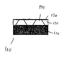
Detailed description of the invention
Fig. lA is a top view of an identification chip for identifying an object
located in a
liquid, according to the invention. Fig. 1B is a cross sectional view of the
identification chip along axis A-A in fig. lA.
CA 02468486 2004-05-26
WO 03/046801 PCT/N002/00448
3
The chip comprises and is composed of an acoustic resonator 100, which
exhibits a
number of distinct resonant frequencies, where the combination of resonant
frequencies is unique to the identification chip. This permits the
identification chip
to be identified by exposing the chip to an acoustic polling signal, measuring
an
acoustic response signal and analysing the frequency of the response signal.
The resonator 100 comprises a cavity-forming part 110, 120 and a membrane 130.
The acoustic resonant frequencies for the resonator are determined by the six
cavities 140 enclosed by the cavity-forming part 110, 120 and the membrane
140.
The cavity-forming part 110, 120 is composed of a substrate 110 with an upper
surface, and an etchable disc 120 with a lower surface that is attached to the
upper
surface of the substrate 110. The substrate 110 is composed of a glass wafer,
while
the etchable disc 120 is made of silicon.
The upper surface of the etchable disc 120 is also attached to the lower
surface of
the membrane 130. The etchable disc 120 further comprises six, through-going,
circular openings between the lower and upper surfaces, with the result that
each of
the six cavities is enclosed by the substrate, the corresponding through-going
opening and the membrane.
Fig. 1B is a cross sectional view of the identification chip along axis A-A in
fig.
lA. The figure therefore illustrates the three of a total of six cavities 140
included
in the resonator 100 that are intersected by axis A-A. Fig. 1B illustrates
that each
cavity is enclosed by the substrate 110, the etchable disc 120 and the
membrane
130.
Fig. lA illustrates that the resonator 100 may be rectangular in shape, viewed
from
above. In a practical embodiment the shape may be more elongated or rod shaped
than that illustrated in fig. lA. This offers practical advantages when
inserting an
identification chip in an organism such as 'a fish, where the insertion should
advantageously be performed through a hole with the smallest possible cross
section.
Figs. lA-1B illustrate that the cavities are of different sizes, particularly
different
cross sections, and more specifically different diameters where each cavity's
cross
section is circular.
The number of cavities is decisive for the number of possible coding
combinations.
If the number of cavities with distinct resonant frequency is designated as n,
the
number of possible coding combinations is 2n-1.
Resonators with different combinations of cavity cross section can be
manufactured
directly, or chips can be produced with a full set of cavity combinations,
which are
CA 02468486 2004-05-26
WO 03/046801 PCT/N002/00448
4
subsequently encoded by destroying the membranes for those cavities that are
not to
be included in the code.
Figs. 2A-2E illustrate cross sections of different embodiments of an
identification
chip according to the invention.
Figure 2A illustrates a cross section of a first embodiment of an
identification chip
for implanting in a living organism such as a fish.
The identification chip comprises an acoustic resonator 100, which exhibits a
number of distinct resonant frequencies, where the combination of resonant
frequencies is unique to the identification chip. This permits the
identification chip
to be identified by exposing the chip to an acoustic polling signal, measuring
an
acoustic response signal and analysing the frequency of the response signal.
The resonator 100 comprises a cavity-forming part, which in the embodiment in
fig.
2A is composed of a substrate in the form of a glass wafer 110 and an etchable
part
in the form of a silicon wafer 120. The lower surface of the silicon wafer 120
is
attached to the upper surface of the glass wafer 110 by means of anodic
bonding.
The silicon wafer 120 comprises two through-going openings between the lower
and upper surfaces.
The silicon wafer's 120 upper surface is also attached to the lower surface of
a
membrane 130 made of silicon nitride. A membrane is preferably employed with
moderate prestressing, which is typically of the order of 50MPa - 500MPa,
preferably in the range 100MPa - 300MPa.
The walls of the through-going openings are sloping, with the result that the
opening on the lower~surface of the silicon wafer is larger than the opening
on the
upper surface. This shape is the result of the manufacturing process, which is
based
on a silicon nitride membrane, to which an all-enveloping silicon layer is
attached
in advance, and subsequent anisotropic wet etching by means of potassium
hydroxide I~OH for removal of the silicon material corresponding to the
resulting
openings. Such a process results in square membrane sections with sloping
(54.7°)
side walls.
The glass wafer 110, the silicon wafer 120 and the membrane 130 thereby
enclose
two cavities 140 of different size. These cavities determine two distinct
resonant
frequencies for the resonator 100.
Figure 2B illustrates an embodiment of the identification chip where the
silicon
wafer 120 has only one through-going opening between the lower and upper
surfaces, with the result that the chip comprises one cavity. The membrane's
130
lower surface, however, comprises areas 122 covered by silicon material. Those
membrane sections not covered by silicon on the lower surface' are of a
different
CA 02468486 2004-05-26
WO 03/046801 PCT/N002/00448
size. On account of this, the chip 100 will still exhibit several different
resonant
frequencies as long as the rigidity in the beams 122 is sufficiently great to
enable
the membrane sections to vibrate fairly independently of one another.
This embodiment requires a smaller total substrate area, and therefore allows
better
5 use to be made of the silicon material compared with the embodiment in fig.
2A.
However, a certain amount of acoustic coupling will occur between the
uncovered
membrane sections, and the chip will have a lower value for acceptable maximum
pressure on account of lack of attachment of the membrane at several points.
Figure 2C illustrates an embodiment of the identification chip that resembles
the
embodiment in figs. lA-S, where the silicon wafer 120 has four through-going
openings between the lower and upper surfaces, with the result that the chip
comprises four cavities.
The walls of the through-going openings are perpendicular to the common
horizontal direction for the glass wafer, the silicon wafer and the membrane,
with
the result that the opening on the lower surface of the silicon wafer is
almost
identical to the opening on the upper surface. This shape is the result of the
production process, which is based on a silicon nitride membrane, to which a
completely covering silicon layer is attached in advance, and a subsequent
dry,
reactive ionic etching (RIE etching) for removal of the silicon material
corresponding to the resulting openings. Such a process results in membrane
sections with approximately straight side walls. This provides very good
utilisation
of space, but requires a more complicated production process.
Fig. 2D illustrates an identification chip where the cavity-forming part is
composed
solely of a substrate in the form of a glass wafer 110. The upper surface of
the glass
wafer 110 has four recesses with different areas, but the same depth. The
lower
surface of the membrane 130 is attached to the upper surface of the glass
wafer 110.
This results in each of the four cavities being enclosed by a recess and a
section of
the membrane 130.
The first stage in the manufacture of this embodiment is to form the recesses
140 in
the glass wafer by means of etching. The silicon nitride membrane is then
affixed,
being initially attached to a silicon wafer, whereupon all the silicon
material is
removed by etching.
In fig. 2E the upper surface of the membrane 130 is attached to the lower
surface of
a silicon wafer 150, which has through-going openings. Each opening coincides
with one of three etched recesses in the glass wafer 110.
CA 02468486 2004-05-26
WO 03/046801 PCT/N002/00448
6
In all the embodiments in figs. 2A-2E, the cavities 140 preferably contain a
vacuum. It is also possible to replace the vacuum with a gas, in which case it
will be
advantageous if the said gas is air or a gas with large "heavy" molecules.
The object of this is to be able to restrict diffusion as much as possible.
Examples of
"heavy" gases are fluorated hydrocarbons and SF6.
In all the embodiments in figs. 2A-2E, the identification chip advantageously
comprises a reference cavity with a predefined resonant frequency fox use in
calibration and compensation for pressure and temperature variations. The
earlier
statement that the cavities may contain a vacuum, air or another gas also
applies to
the reference cavity.
In all the embodiments in figs. 2A-E, the identification chip may
advantageously
comprise an encapsulation (not shown) round the resonator. The encapsulation
is
preferably made of a biocompatible material such as, e.g., water as ice or
another
material with acoustic properties resembling the properties of water, thus
ensuring
that the encapsulation does not substantially influence the acoustic
properties of the
resonator. Alternatively, the chip may be composed of the resonator without
encapsulation.
Fig. 3A illustrates a block diagram for an identification system where
identification
chips according to the invention are employed.
The system is based on the transmission of an acoustic polling signal and
measurement of an acoustic response signal. An identification chip comprises a
resonator that exhibits a combination of resonant frequencies. By comparing
the
characteristics of the transmitted and detected signals, the system is
arranged to
derive a unique identity associated with the identification chip.
The object, usually a fish or another living organism, is tagged with an
identification chip 100 according to the invention. A transmitting transducer
30 is
arranged to transmit acoustic waves towards the object 10, and a receiving
transducer 40 is arranged to receive acoustic waves from the object 10.
Between the object 10 and each transducer 30, 40 is a liquid, usually water,
including salt water.
The system further comprises a control unit 50, which controls a signal
generator 34
and a recording unit 46. The signal generator 34 is arranged to provide a
signal that
includes frequencies in the ultrasound range, especially in the frequency
range
20kHz - 3MHz, and more preferably between 100kHz and 300kHz. The signal may
be narrow band, the control unit being arranged to vary or sweep the signal
frequency over a wider area over a period of time. Alternatively the signal
may be
CA 02468486 2004-05-26
WO 03/046801 PCT/N002/00448
7
broad band with a known spectrum. The signal is amplified by means of an
amplifier 32, which supplies an amplified signal to the transmitting
transducer 30.
The receiving transducer 40 is arranged to intercept a reflected or scattered
acoustic
signal, which is influenced by the identification chip 100 in the object 10.
The signal from the receiving transducer 40 is fed to an amplifier 42, and the
output
signal herefrom is converted to a digital signal by means of the analog-
digital
converter 44. The digital signal is fed to the recording unit 46, which also
receives a
control signal from the control unit 50. The recording unit comprises a
computer
with a program, which on execution compares. information on the transmitted
acoustic signal and the received acoustic signal, and which, by establishing
the
resonant frequency derives an identification associated with the
identification chip
100.
Fig. 3B illustrates an alternative embodiment of the system, where instead of
a
separate transmitting transducer 30 and receiving transducer 40, a combined
transmitting and receiving transducer 36 is employed, which is arranged to act
as
transmitter and receiver in different periods. The transducer 36 is connected
to a
transmitting/receiving switch 38, which directs a signal that has to be
supplied by
the amplifier 32 to the transducer 36 when it is used as a transmitter, or it
directs a
signal received by the transducer when it is used as a receiver, to the
amplifier 42.
In fig. 3B a reflector 12 is also provided on the opposite side of the object
10. This
causes the~signal received by the transducer 36 to be transmitted first
through the
obj ect, including the identification chip 100, and then reflected by the
reflector. The
system may also be implemented without reflector 12.
Other combinations and alternatives are possible for the system. For example,
the
measuring set-up with a common transmitting and receiving transducer 36 may be
employed in the measuring arrangement without a reflector as illustrated in
fig. 3A.
Based on fig. 3A, another variant is to place a transmitting and receiving
transducer
on opposite sides of the object. In order to cover a wider total frequency
range, it
may also be expedient to use more than one transmitting and/or receiving
transducer
with different crossover frequency ranges or centre frequencies.
Fig. 4A illustrates a cross sectional view of an identification chip adapted
for easy
insertion in a fish.
The identification chip 1 comprises an acoustic resonator 100 according to any
of
the embodiments described above. The resonator may also comprise an
encapsulation, as mentioned above.
The chip 1 further comprises a pointed sheath 200 made of a material that is
capable
of melting, dissolving or breaking down in the living organism. Use is
preferably
CA 02468486 2004-05-26
WO 03/046801 PCT/N002/00448
8
made of ice. The sheath 200 simplifies the insertion of the identification
chip in the
organism.
Fig. 4B illustrates a cross sectional view of a variant of an identification
chip
adapted for easy insertion in a fish.
The identification chip comprises an acoustic resonator 100 according to any
of the
embodiments described above. The resonator may also comprise an encapsulation
as
mentioned above.
The chip 1 further comprises a needle-shaped extension part 202 made of a
material
that is capable of melting, dissolving or breaking down in the living
organism. Use
is preferably made of ice. This extension part 202 simplifies the insertion of
the
identification chip in the organism.
Figs. SA-SD illustrate cross sectional views of sections of a resonator in an
identification chip according to the invention, manufactured by means of
surface
micromachining.
In each of the figures SA-SD one of several cavities in an acoustic resonator
100 in
an identification chip is illustrated for identification of an object located
in a liquid.
The acoustic resonator 100 exhibits a number of distinct resonant frequencies,
where the combination of resonant frequencies is unique to the identification
chip.
The resonator 100 comprises a cavity-forming part 110 and a membrane 130. The
acoustic resonant frequencies are determined by the at least one cavity 140,
which is
enclosed by the cavity-forming part 110 and the membrane 130. The resonator
100
is manufactured by surface micromachining.
The cavity-forming part 110 is preferably a substrate of silicon, but glass
may be an
alternative possibility. The production is based on an Si wafer, on which the
desired
structures are formed by depositing films, patterning them and etching from
the
same side of the wafer all the time. An important feature in these processes
employed is so-called sacrificial layers, which are layers inserted in the
structure to
enable overlying layers to be later detached from those located below by
etching
away the sacrificial layer. The sacrificial layer must be able to withstand
the
processing stages the wafer has to undergo from its being deposited until it
is etched
away, e.g. the heating that is necessary in order to give following layers the
desired
characteristics. The sacrificial layer also has to be capable of being removed
by
etching without damaging other parts of the wafer. For these purposes the
sacrificial
layer normally consists of a more or less doped silicon oxide, or
alternatively a
photoresist or a metal.
The resonator 100 may be manufactured by first depositing a sacrificial layer
in the
form of a silicon oxide on a flat Si wafer. Alternatively, a glass wafer may
be
CA 02468486 2004-05-26
WO 03/046801 PCT/N002/00448
y
employed. The sacrificial layer is further patterned in such a manner that it
assumes
the form of the desired cavities 140. A film then has to be applied that has
to form
the membrane 130, preferably consisting of polycrystalline silicon
(polysilicon) or
silicon nitride. The sacrificial layer is then removed by etching. This is
generally
performed by etching one or preferably many small holes in the membrane 130,
through which the etching agent can reach the sacrificial layer. These holes
must be
sealed later, which can be done by applying a thicker layer of the membrane
material, or by placing the openings of the sacrificial layer outside the
actual
membranes in "passages" of the sacrificial material out from the actual
cavities. The
holes can then be sealed by putting on material only near the holes and
letting the
actual membrane be as it was after the initial depositing. It will often be
easier to
control the final membrane thickness in this manner.
Fig. SA illustrates a cavity 140 in a resonator 100 manufactured by means of
surface
micromachining. The membrane 130 has a raised portion, while the substrate 110
is
flat. In the manufacture of this embodiment, a sacrificial layer of, e.g.
silicon oxide
is first deposited uniformly over the entire Si wafer. This is then patterned
by means
of etching with the result that only the part of the sacrificial layer
corresponding to
the desired cavity 140 is left. The etching agent does not attack the
substrate wafer,
with the result that the substrate 110 remains flat after the etching process.
A
membrane film is deposited over the entire wafer. The membrane film is then
opened into the sacrificial layer, the sacrificial layer is etched out, and
the etched
holes sealed.
Fig. SB also illustrates a cavity 140 in a resonator 100 manufactured by
surface
micromachining. The membrane 130 has a raised portion, while the substrate 110
has a recess in the area intended to define the cavity 140. This embodiment is
manufactured by firstly covering the substrate 110 with a thin silicon nitride
film,
which is removed in the area intended to define the cavity 140. The wafer is
then
heated by steam, with the result that a silicon dioxide layer is grown where
the
nitride has been removed. The silicon dioxide layer here constitutes the
sacrificial
layer. The Si nitride can then be removed. The actual membrane film (e.g.
silicon
nitride) is then deposited over the entire wafer. It is then opened up into
the
sacrificial layer, this is etched out, and the etched holes are sealed. Since
the
oxidation of the Si wafer consumed a little of the Si material, the cavity 140
appears
partially sunk into the Si wafer. The embodiment in fig. SB is akin to the
embodiment illustrated in fig. 2D, but in the description of fig. 2D the
substrate
material is specified as glass, and this may involve the need for "silicon
fusion
bonding" in order to achieve sufficiently good bonding between substrate and
membrane or film.
Fig. SC also illustrates a cavity 140 in a resonator 100 manufactured by
surface
micromachining. The membrane 130 has a raised portion, while the substrate 110
CA 02468486 2004-05-26
WO 03/046801 PCT/N002/00448
lU
also has a raised portion, albeit a lower one, in the area intended to define
the cavity
140. In manufacturing this embodiment, a sacrificial layer is first deposited
or
grown uniformly over the entire Si wafer. This is then patterned by etching.
If an
etching technique is employed that also attacks the Si wafer, the final
resonator will
appear somewhat raised above the surface of the wafer. The membrane film is
deposited over the entire wafer, whereupon the sacrificial layer is etched out
as
indicated above.
Fig. SD also illustrates a cavity 140 in a resonator 100 manufactured by
surface
micromachining. Here the membrane 130 is flat, in the same way as the
embodiments illustrated in figs. 2A-2E. The substrate 110 has a recess in the
area
that defines the cavity 140. In order to achieve this structure, the membrane
film is
transferred from a second substrate. In this case a recess first has to be
etched out,
or the areas round the recess have to be built up, and a flat film is then
bonded on
the top. This is accomplished in practice by the film being formed on a second
substrate, which is then bonded to the original wafer with the film facing the
wafer.
The supporting wafer for the film can then be etched away.
It is true for all the embodiments of the invention that the resonant
frequency is
influenced by flexural strength and elasticity in the membrane, size and shape
of the
membrane, the attachment of the membrane along the periphery and the height h
of
the cavity under the membrane if this is gas-filled with a pressure p where
hlp < 10
~,m/atm. If, however, the cavity is evacuated, the height h will not be
important for
the resonant frequency, provided the height la is sufficiently great (la> 1
Vim) to
ensure that the membrane does not strike the bottom of the cavity during
excitation
by the polling signal.
It will be appreciated that many possibilities exist for layout of the
cavities on the
identification chip. For example, the cavities may be arranged in 1, 2, 3 or 4
rows.
In an elongated or rod-shaped embodiment, which is preferred for a chip for
implanting iri a fish, one single row will be appropriate.