Note: Descriptions are shown in the official language in which they were submitted.
CA 02469428 2010-12-15
53135-4
VOLTAGE CONTROLLER FOR SWITCHING POWER SUPPLIES
BACKGROUND OF THE INVENTION
1. Field of the Invention
The invention relates in general to voltage control and in particular to
digital
voltage control for high frequency voltage regulators.
2. Statement of the Problem
Analog voltage controllers are widely used in cooperation with power
converters for DC-DC (direct-current to direct-current) converters. Analog
controllers
are fast and can generally be built with widely available analog components.
However, the operation of analog controllers depends on the precision of the
individual .components included therein. Accordingly, considerable effort must
be
expended to ensure selection of analog components adhering to very precise
quality
1 `5 control standards. Moreover, even after such careful selection, the
behavior of
analog components is subject to variations in manufacturing processes,
operating
temperatures, and degradation over time. Moreover, analog designs are not
readily
realized employing existing automated design methods. Accordingly, the design
of
analog controllers tends to be time-consuming and labor intensive.
Some existing voltage controllers include one or more digitally implemented
components. However, the digital components implemented in existing voltage
controllers have not performed as desired. For example, digital signal
processors
(DSPs) have been implemented to perform arithmetic operations, such as
multiplication, as part of the operation of a compensator, within a voltage
controller.
However, these DSP implementations are slow, take up a lot of space, and are
excessively complex for the task being performed. Moreover, because the DSPs
require digital data to operate, their implementation incurs the need for
large and
energy-expensive analog to digital converters (ADCs). The ADCs included in
such
1
CA 02469428 2004-06-04
WO 03/050637 PCT/US02/39189
controllers are precision analog components which take up an inordinate amount
of
valuable space on chips, consume large amounts of power, and are subject to
the
same temperature-induced and process-induced performance variations as are
analog components of the older existing controllers.
Accordingly, the art of voltage control would benefit from the provision of a
voltage controller which is small, energy and space-efficient, and whose
performance is not dependent of the temperature and process variations of
individual
controller components.
SUMMARY OF THE INVENTION
The present invention advances the art and helps to overcome the
aforementioned problems by providing a small, fast, accurate, energy-efficient
voltage controller, the performance of which is independent of temperature-
variations
and other variations in the characteristics of component parts. In the
preferred
embodiment, all functions of the inventive controller are implemented
employing
digital logic gates, thereby avoiding the need for, and the performance
variations of,
precision analog components. In the preferred embodiment, the digital logic
gates
forming the inventive controller can be effectively modeled employing existing
electronic design automation, such as hardware description languages (HDLs),
thereby simplifying and shortening design time.
A delay line ADC, preferably consisting exclusively of digital logic gates,
preferably provides a digitally encoded error signal indicative of a disparity
between
an output voltage and a reference voltage. The delay line ADC disclosed herein
thereby preferably performs the function associated with analog voltage
comparison
devices in existing analog controllers. Separately, the delay line ADC
preferably
performs the function of a combination of an ADC and a digital voltage
comparison
device in existing partially digitally implemented voltage controllers.
In the preferred embodiment, a hybrid digital pulse width modulator and
compensator are also digitally implemented. In the preferred embodiment, the
compensator includes a lookup table for rapidly converting a digital error
signal from
the delay line ADC into a digital control signal, which is preferably a
digitally
expressed duty ratio, provided as output from the compensator. In the
preferred
embodiment, a digital pulse width modulator receives the compensator-provided
digital control signal as input and converts this digital signal into a duty
ratio-
controlled time varying control signal as output from the controller.
Preferably, the
2
CA 02469428 2010-12-15
53135-4
controller output is provided to a power converter to increase or decrease the
regulator output voltage, depending on the results of a comparison between the
output voltage and the reference voltage.
The advantages of implementing the digital controller technology disclosed
herein include the following. A fully digital controller could be very
attractive in high-
frequency, low-to-medium power DC-DC converters because of the inherently
lower
sensitivity to process and parameter variations, the ready programmability of
various
controller performance characteristics, the reduction or elimination of
passive
components for tuning, and the ease of integration with other digital systems.
A
benefit arising from compensator programmability and from the absence of the
need
to tune passive components is that the same controller hardware could be used
with
a range of power converter configurations and power-stage parameter values. In
addition, with digital controller implementation, it is possible to implement
control
schemes that are impractical for analog controller designs.
For example, it is desirable to have the ability to precisely match phase-
shifted duty ratios to a simple, robust control for voltage regulator modules
(VRMs)
using a dedicated digital controller IC (integrated circuit). In transformer-
isolated DC-
DC converters, digital signal transmission through the isolation can be used
to
address limited bandwidth and/or large gain variations associated with
standard
analog approaches. In general, more sophisticated control methods could be
used
to achieve improved dynamic responses.
Another advantage of the digital approach is that well established and
automated digital design approaches can be applied. A controller design may be
described at the functional level using a hardware description language (HDL).
Preferably, synthesis, simulation, and verification tools are available to
target the
design to implementation to standard cell ASICs (application-specific
integrated
circuits) or FPGAs (field programmable gate arrays) from the HDL description.
The
design can then be implemented employing different manufacturing processes,
integrated with other digital systems, or modified to meet updated
specifications. In
contrast to analog IC controller realizations, the digital controller design
preferably
scales well, and can thus take advantage of advances in fabrication
technologies,
without design alteration.
3
CA 02469428 2010-12-15
53135-4
According to one aspect of the present invention, there is provided a
voltage controller comprising: a compensator including a lookup table for
determining
a digital control signal based on a digital error signal; a modulator
operative to
provide a power control signal in response to said determined digital control
signal;
and a delay line analog to digital converter operative to compare a converter
voltage
to a reference voltage and generate said digital error signal indicative of a
difference
between said compared voltages; wherein said compensator, said modulator, and
said delay line of said controller include no passive electronic components.
According to another aspect of the present invention, there is
provided a voltage controller comprising: a compensator including a lookup
table
for determining a digital control signal based on a digital error signal; a
modulator
operative to provide a power control signal in response to said determined
digital
control signal; and a delay line analog to digital converter operative to
compare a
converter voltage to a reference voltage and generate said digital error
signal
indicative of a difference between said compared voltages; wherein said
controller
is implemented entirely with digital logic gates.
According to still another aspect of the present invention, there is
provided a voltage controller comprising: a compensator including a lookup
table
for determining a digital control signal based on a digital error signal; a
modulator
operative to provide a power control signal in response to said determined
digital
control signal; and a delay line analog to digital converter operative to
compare a
converter voltage to a reference voltage and generate said digital error
signal
indicative of a difference between said compared voltages; wherein all
energy-storing components in said controller are digital logic gates.
According to yet another aspect of the present invention, there is
provided a voltage controller comprising: a compensator including a lookup
table
for determining a digital control signal based on a digital error signal; a
modulator
operative to provide a power control signal in response to said determined
digital
control signal; and a delay line analog to digital converter (ADC) operative
to
compare a converter voltage to a reference voltage and generate said digital
error
signal indicative of a difference between said compared voltages; wherein said
delay line ADC comprises a delay cell array.
3a
CA 02469428 2010-12-15
53135-4
According to a further aspect of the present invention, there is
provided a voltage controller comprising: a compensator including a lookup
table
for determining a digital control signal based on a thermometer code digital
error
signal; a modulator operative to provide a power control signal in response to
said
determined digital control signal; and a delay line analog to digital
converter (ADC)
operative to compare a converter voltage to a reference voltage and generate
said
thermometer code digital error signal indicative of a difference between said
compared voltages.
According to yet a further aspect of the present invention, there is
provided a voltage controller comprising: a compensator including a lookup
table
for determining a digital control signal based on a digital error signal; a
modulator
operative to provide a power control signal in response to said determined
digital
control signal; and a delay line analog to digital converter operative to
compare a
converter voltage to a reference voltage and generate said digital error
signal
indicative of a difference between said compared voltages; wherein said
modulator comprises a delay line operative to determine a component of a
pulse-on period for said power control signal.
According to still a further aspect of the present invention, there is
provided a voltage controller comprising: a compensator including a lookup
table for
determining a digital control signal based on a digital error signal; a
modulator
operative to provide a power control signal in response to said determined
digital
control signal; and a delay line analog to digital converter operative to
compare a
converter voltage to a reference voltage and generate said digital error
signal
indicative of a difference between said compared voltages; wherein said
modulator
comprises; a counter operative to determine a first component of a pulse-on
period
for said power control signal; and a delay line operative to determine a
second
component of said pulse-on period for said power control signal.
According to another aspect of the present invention, there is provided
a method for controlling voltage, the method comprising: comparing a converter
output voltage with a reference voltage; generating a digital error signal
indicative of
a result of said comparing; and providing a power control signal indicative of
said
3b
CA 02469428 2010-12-15
53135-4
generated error signal, wherein signal processing of said comparing, said
generating, and said providing are performed entirely with digital logic
gates.
According to yet another aspect of the present invention, there is
provided a method of controlling a regulator output voltage, the method
comprising: receiving said regulator output voltage; converting said received
regulator output voltage into a digital error signal employing a delay line
analog to
digital converter (ADC); and adjusting said regulator output voltage to an
adjusted
regulator output voltage based on said digital error signal; wherein said
converting
comprises: powering a delay cell array of said delay line ADC with said
received
regulator output voltage; measuring a speed of test signal propagation through
said powered delay cell array; and generating said digital error signal
indicative of
said measured test signal propagation speed.
The above and other advantages of the present invention may be better
understood from a reading of the following description of the preferred
exemplary
3c
CA 02469428 2004-06-04
WO 03/050637 PCT/US02/39189
embodiments of the invention taken in conjunction with the drawings in which:
BRIEF DESCRIPTION OF THE DRAWINGS
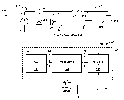
FIG. 1 is a block diagram of a voltage regulator including a digital voltage
controller according to a preferred embodiment of the present invention;
FIG. 2 is a plot of the transient response of output voltage and output
current
obtained with the regulator of FIG. 1;
FIG. 3 is a block diagram of the operation of the digital voltage controller
of
FIG. 1;
FIG. 4 is a block diagram of the pulse width modulator included in the digital
voltage controller of FIG. 1;
FIG. 5 is a plot of waveforms of signal values of the pulse width modulator of
FIG. 4;
FIG. 6 is a plot of duty ratio output as a function of digital input for the
pulse
width modulator of FIG. 4;
FIG. 7 is a block diagram of the delay line ADC included in the voltage
controller of FIG. 1;
FIG. 8 is a schematic diagram of a delay cell ADC corresponding to the delay
cells included in the delay line of FIG. 7;
FIG. 9 is a plot of timing waveforms for tap signals of the delay line ADC of
FIG. 7;
FIG. 10 is a plot of the conversion characteristic of the delay line ADC of
FIG.
7;
FIG. 11 is a block diagram of a preferred digital calibration scheme for the
delay line ADC of FIG. 7;
FIG. 12 is a plot of timing waveforms of the calibration scheme of FIG. 11;
FIG. 13A is a plot of the measured load voltage regulation against load
current for the voltage regulator of FIG. 1;
FIG. 13B is a plot of the measured load voltage regulation against supply
voltage for the voltage regulator of FIG. 1; and
FIG. 14 is a block diagram of the function of encoder 730 included in the
delay
line ADC 700 of FIG. 7.
DETAILED DESCRIPTION OF THE PREFERRED EMBODIMENT
In this disclosure, a transistor terminal is either the source or drain of a
field
effect transistor (FET) or the emitter or collector of a bipolar junction
transistor (BJT).
4
CA 02469428 2004-06-04
WO 03/050637 PCT/US02/39189
Herein, a comparator is any device that receives two voltage values and which
provides as output a signal indicative of a difference between the two
received
voltage values. Herein, the terms "comparator" and "voltage comparator" are
used
interchangeably. In this disclosure, energy-storing components include both
analog
and digital devices, including for instance, capacitors, inductors and powered
digital
logic gates. The term "energy-storing components" is intended to exclude
wiring and
other conductive apparatus operative merely to connect one electronic
component to
another. Herein, a resistor is a device having resistance concentrated in a
lump
form. Herein, a resistor does include wiring or other conductive links between
electronic components. Herein, an electronic memory is a digital electronic
storage
device able to supply stored values in response to an identification of an
address in
the electronic memory of the stored values. Herein, a digital electronic
calculator
may include a digital electronic storage device and/or digital devices for
performing
arithmetic operations including any one or more of addition, subtraction,
multiplication, and/or division.
Herein, a signal tap array may include any number of signal taps. A signal tap
array preferably includes a plurality of signal taps, each tap connected to
one delay
cell within an array of delay cells. However, a signal tap array may include
signal
taps connected to only a subset of delay cells within a delay cell array.
Herein,
binary digital code is conventional digital code in which a sequence of bits
identifies
coefficients of values equal to number "2" raised to different powers. For
example,
digital code "101" corresponds to 1 = 1 + 0 = 2 + 1 = 4 = 5. Binary digital
code is
distinguished from "thermometer code" in which each bit in a sequence is of
equal
numerical weight.
FIG. 1 is a block diagram of a voltage regulator 100 including a digital
voltage
controller 150 according to a preferred embodiment of the present invention.
Regulator 100 preferably includes power converter 200 and controller 150.
Power
converter ("converter") 100 is preferably a synchronous buck converter. Power
converter preferably includes gate driver 204 which is connected to the gate
of
transistor switch 202, a first terminal of which transistor is connected to
supply
voltage 102 positive node 114 and a second terminal of which is connected to
node
116. Gate driver 206 provides an output connected to the gate of transistor
switch
208, one terminal of which transistor is connected to supply voltage negative
node
112 and the other terminal of which is connected to node 116. Inductor 210 is
5
CA 02469428 2004-06-04
WO 03/050637 PCT/US02/39189
preferably located between node 116 and node 118. Capacitor 212 is preferably
located between node 118 and node 112.
In the embodiment of FIG. 1, power converter 200 is connected to supply
voltage Vg 102 and produces output voltage Vo 104 which is connected between
node 118 and node 112 of converter 200 across load 110, which is connected in
parallel with capacitor 212. The operation of converter 200 is known in the
art and is
therefore not discussed in detail in this disclosure. It will be appreciated
that the
present invention is not limited to the design of converter 200. A wide range
of
designs and principles of operation may be incorporated into converter 200
which
would not affect the operation of the preferred embodiment of controller 150.
It will
be appreciated that converter 200 of FIG. 1 is merely one of many converter
designs
which could be employed in conjunction with controller 150.
In the preferred embodiment, controller 150 includes delay line ADC 700,
compensator 300, and pulse width modulator (PWM) 400, which is preferably a
hybrid digital pulse width modulator. Preferably, voltages Vsense 108 and Vref
106 are
inputs to controller 150, and, in particular, to delay line ADC 700. Equipment
(not
shown) for providing Vref 106 is preferably not part of controller 150.
Preferably,
external memory 160 is available to supply information to compensator 300,
when
needed. Delay line ADC 700 preferably serves as a voltage comparator in the
embodiment of FIG. 1. While delay line ADC 700 is the preferred voltage
comparator in the present application, the current invention is not limited to
the use
of delay line ADC 700 for generation of a signal indicative of a voltage
difference
between voltages Vsense 108 and Vref 106. In alternative embodiments, a range
of
devices, either analog or digital, for providing a signal indicative of a
voltage
difference between two voltage sources may be employed in controller 150, and
all
such variations are intended to be included within the scope of the present
invention.
In this embodiment, converter 200 and controller 150 form a closed-loop
feedback system 100, to preferably regulate output voltage VO 104 to match a
stable
voltage reference Vref 106 (or a scaled version of the reference) over a range
of input
voltage 102 values and load currents, and over a range of process and
temperature
variations. In this embodiment, output voltage 104 is sensed and compared to
Vref
106. Digital error signal 152 is preferably transmitted to compensator 300.
Compensator 300 output (digital control signal) 154 is the input to pulse
width
modulator 400, which in turn preferably produces a constant frequency variable
duty
6
CA 02469428 2004-06-04
WO 03/050637 PCT/US02/39189
ratio signal (power control signal) 156 to control the switching power
transistors 202,
208. The preferred embodiment of a digital controller architecture to
implement this
control scheme is shown in FIG. 3.
Preferably, Vsense 108 is a scaled version of Vo 104. Expressing this
mathematically, we have Vsense = HVo. However, in this disclosure, for the
sake of
simplicity, H is considered to have a value of 1. Thus, for the remaining
discussion,
Vsense 108 and V0 104 have the same value. Preferably, Vo 104 is sampled by an
A/D (analog to digital) converter to produce digital error signal e(n) 152.
Preferably,
sampling of Vo 104 occurs once per switching period Ts. Here, the index value
of "n"
refers to the current switching period.
Generally, effective voltage regulation generally requires that V0(t) 104
remain
within a defined range of Vref 106, from Vref - (AV0)max/2 to Vref +
(AV0)max/2.
Otherwise stated, the permissible range for steady-state output voltage 104 is
V. =
Vref AV0/2. To maintain Vo 104 within the permissible range, the analog
equivalent
of the least significant bit (LSB) in the A/D characteristic should not be
greater than
the desired magnitude of AV0. Preferably, the specifications for L\V0 and
(OV0)max are
such that only a few digital values are needed to represent the magnitude of
the
analog voltage error, which is equal to Vref 106 - Vsense 108.
FIG. 3 is a block diagram of the operation of digital voltage controller 150
of
FIG. 1. In the embodiment of FIG. 3, the digital representation of error
signal 152
assumes one of nine values, from -4 to +4 (decimal). Although ADC 158
preferably
has sufficiently fine resolution to accurately regulate Vo 104, only a few
bits are
needed to represent digital error signal e(n) 152. In the preferred
embodiment, the
value of digital error signal 152 is used as a lookup table address. Thus, any
arbitrary association may be established between the magnitude of digital
error
signal 152 and the magnitude of the numerical entries located at the lookup
table
address pointed to by the digital error signal 152 value. Table 1, located
later in this
document, identifies a preferred embodiment correlation between digital error
signal
values and the magnitude of the control signal desired. Herein, the "digital
error
magnitude" is a value that corresponds to the magnitude of the disparity
between the
measured voltages. Preferably, a digital error signal corresponds to the
lookup table
address at which its digital error magnitude is located.
A novel delay line ADC configuration 700 that takes advantage of the required
static A/D characteristic and which lends itself to a simple digital
implementation is
7
CA 02469428 2010-12-15
53135-4
described in connection with FIG. 7. It will be appreciated that delay line
ADC 700 is
the preferred although not the only available embodiment of ADC 158.
In addition to relaxing the requirements for ADC 158, the ability to represent
error signal 152 with a limited number of bits enables a simplified
implementation of
the next controller component - compensator 300. Preferably, compensator 300
uses the value of digital error signal 152, optionally along with stored
values 312
and 314 of signal 152 from previous cycles, to calculate a digital control
signal 154, which in the preferred embodiment, is a digitally expressed duty
ratio
of a constant frequency signal.
The computation within compensator 300 may be established in accordance
with established digital control theory. However, standard implementation of
linear
control laws in compensator 300 would generally involve the use of digital
adder(s)
and/or digital multiplier(s), which devices increase the size of controller
150 and
which tend to increase the clock frequency requirements for controller 150. To
beneficially exploit the fact that only a small number of bits are needed to
represent
digital error signal 152, the preferred embodiment of compensator 300 instead
calculates duty ratio 154 using look-up tables 302, 304, and 306 and adder
318. Preferably, the
current and the previous values 312 and 314 of digital error signal 152 in
data latches 308 and
310 serve as address(es) from which values may be obtained in lookup tables
302, 304, and
306. Since digital error signal 152 preferably assumes only a small number of
values, the
number of entries in the lookup tables 302, 304, and 306 is correspondingly
small.
Consequently, the implementation of tables 302, 304, and 306 requires only
minimal
real estate on a chip. Moreover, the calculation of duty ratio 154 can
preferably be
accomplished in a small number of system clock 120 cycles. Although the
discussion of FIG. 3 is directed to an embodiment including three lookup
tables and
one adder, it will be appreciated that more than one adder could be employed
and
that fewer or more than three lookup tables could be employed.
Preferably, compensator 300' can be programmed to perform different control
algorithms by adjusting the values of entries in lookup tables 302, 304, and
306.
One control algorithm for determining the current duty ratio d(n + 1) 322
supported
in the embodiment of FIG. 3 is described as follows:
(1) d(n + 1) = d(n) + a(e(n)) + 13(e(n - 1) + y(e(n - 2)), where a(.), (3(.)
and
y(.) may be either linear or nonlinear functions of digital error signal 152
and d(n) is
the previous duty ratio value 320 in data latch 316. However, a variety of
control
algorithms can be implemented. One additional example is described by-
8
CA 02469428 2010-12-15
53135-4
(2) d(n + 1) = d(n) + ae(n) + be(n - 1) + ce(n - 2),
where a, b, and c are constants and corresponds to a basic PID (proportional,
integral, and derivative) control algorithm. In the design of controller 150,
once the
coefficients a, b and c are selected (to achieve a desired closed-loop
bandwidth and
adequate phase margin, for example), the products a = e, b = e, and c = e are
preferably pre-computed for all possible values of the error "e" and
preferably
programmed into lookup tables 302, 304, and 306 from external memory 160
through
interface 330. As an alternative to using external memory 160, lookup tables
302, 304,
and 306 could be preprogrammed and hard-wired on the chip at design time, or
programmed
from other system components via a suitable interface at run time. Thus,
external
memory 160 is one beneficial approach to supplying data to lookup tables 302,
304,
and 306, but alternatives approaches, as discussed above, are available.
The programmability of compensator 300 preferably enables the same
controller 150 hardware to be used with different power-stage configurations
and
different power-stage parameters by modifying data entries to lookup tables
302,
304, and 306 rather than by making hardware changes. Moreover, compensator
300 preferably enables experimentation with various nonlinear control
algorithms
without requiring the labor-intensive, time-consuming, and inconvenient
replacement
of precise analog components.
FIG. 4 is a block diagram of pulse width modulator 400 included in the digital
voltage controller of FIG. 1. FIG. 5 is a plot of waveforms of various signal
values of
the pulse width modulator of FIG. 4. Pulse width modulator (PWM) 400, which is
preferably a hybrid digital PWM, preferably completes the controller
architecture.
PWM 400 preferably produces the periodic waveform c(t) 156 from duty ratio 154
and preferably controls transistor switches 202 and 208 in power converter 200
therewith. Preferably, PWM 400 may be beneficially employed to achieve high
switching frequency operation and control of Vo 104 within a small, defined
range.
PWM 400 preferably operates as a D/A converter (DAC) in voltage regulator
100. Generally, the PWM 400 resolution determines the available set of output
voltage 104 values. If the PWM 400 resolution is not sufficiently high, an
undesirable
limit-cycle oscillation in the value of Vo 104 can result. If none of the
achievable
output voltages 104 fall into the range of AV0 around Vfef 106, duty ratio 154
will
generally oscillate between two or more values. Avoidance of this limit-cycle
operation may be achieved by ensuring that the output voltage increment that
9
CA 02469428 2010-12-15
53135-4
corresponds to the least-significant bit of duty ratio 154 is smaller than
AV0. This
condition has been evaluated as a function of the steady state input and
output
voltages for different converter configurations.
A high-resolution, high-frequency digital pulse-width modulator (DPWM) can
be constructed using a fast-clocked counter and a digital comparator- To
achieve n-
bit resolution at the switching frequency fs, the desired clock frequency is
2"fs. This
desired clock frequency generally leads to more demanding timing constraints
and
increased power consumption. For example, an 8-bit resolution at the switching
frequency of fs = 1MHz would require a clock frequency of 256MHz. It has been
shown that fine time resolution and much lower power consumption can be
achieved
using a tapped delay-line scheme similar to a ring oscillator that operates at
the
switching frequency. However, this implementation requires a larger-area
digital
multiplexer. The PWM architecture selected for use in the preferred embodiment
is
based on a hybrid delay-line/counter approach. In this approach, n-bit
resolution is
achieved using an n,-bit counter (where n, < n), whereas the remaining nd = n -
n,
bits of resolution are obtained from a tapped delay line.
The embodiment of FIG. 4 is a PWM 400 where 47bit (n = 4) resolution is
obtained using 2-bit counter (n. = 2) 406 and a 4-cell ring oscillator (nd =
2, 2"d = 4)
402 which includes flip-flops 416, 418, 420, and 422 operating as delay cells.
20.: Preferably, at the beginning of a switching cycle, output SR flip-flop
410 is set due to n,-bit
comparator 460 and AND gate 470, and the PWM 400 output pulse c(t) 156 goes
high.
Preferably, a pulse propagates through oscillator 402 at a frequency of 2"`fs
= 4fs which
pulse serves as the clock pulse for the counter 406. The switching period is
preferably
divided into 2nd2 = 16 slots. Preferably, when counter 406 output matches the
top c 25 n, 452 most significant bits of digital input 154 at nc bit
comparator 408 and a pulse
reaches the tap selected by the nd 450 least significant bits of digital input
154, output
flip-flop 410 is reset due to AND gate 472, and the output pulse goes low.
It will be appreciated that resolution employing any number of bits n 450 may
be employed, including a wide range of values for n,, 452 and nd 454 may be
30 employed. Preferably, a "pulse-on" period during which output pulse 156
(power
command signal) is on corresponds to the value of digital input 154. This
"pulse-on"
duration is preferably the. product of the duty ratio, expressed by digital
input 154,
and the switching period (reciprocal of f5i the switching period). In order to
avoid the
very high clock frequencies needed to accurately establish the pulse-on period
with
CA 02469428 2010-12-15
53135-4
high resolution using only a counter and comparator, the pulse-on period is
preferably established by separately establishing two separate components of
the
pulse-on period. For a given switching period, determination of the first and
second
components of the pulse-on period for output signal 156 effectively determines
the
first and second components of the duty ratio for output signal 156.
In the preferred embodiment, a first component, or first portion, of the pulse-
on period is preferably established using a selection n, 452 of the highest
ordered
bits of digital input 154. Counter 406 preferably counts to a value equal to
"2" raised
to the power n, 452 at clock frequency 120. A second component, or second
portion, of the pulse-on period is preferably established using the nd 454
lowest
ordered bits of the original n 450 bits of digital input 154. The second
component of
the pulse-on period is preferably established using a delay line 402 having a
specified number
of flip-flops and outputs 424, 426, 428 and 430. The number of flip-flops used
is preferably
equal to 2 raised to the power nd 454. Preferably, the magnitude of the
digital value of the
sequence of nd 454 bits determines the number of flip-flop delays which form
the
second component of the pulse-on period. This hybrid (combination of counter
and
delay line) approach preferably avoids the need for an extremely high
frequency for
counter 406 while still maintaining high accuracy for the resulting pulse-on
period
during which output signal c(t) 156 is high.
In the exemplary waveforms of FIG. 5, the duty ratio of the output pulse is
11/16. The basic delay cell in ring oscillator 402 of FIG. 4 consists of a
single
resettable flip-flop. Preferably, the delay of each of cells 416, 418, 420,
and 422 and
the number of cells in ring 402 determine the switching frequency f9. To
adjust the
switching frequency, any cell of cells 416, 418, 420, and 422 can be modified
by
inserting additional delay elements between the output of a cell and the input
to a
succeeding cell. The additional delay elements can be standard logic gates, or
gates with adjustable delay, if switching frequency tuning or synchronization
with an
external clock are desired.
The self-oscillating DPWM (digital pulse width modulator) embodiment shown
in FIG. 4 has several desirable properties including a simple HDL description,
an
even number of time slots in a period, an ability to stop and restart the
oscillations on
command (by gating the propagation of the signal through the ring), and
relatively
small size. An experimental prototype chip was designed in which the DPWM had
8-
bit resolution (n = 8) using a 3-bit counter (nc = 3) and a 32-cell long ring
(nd = 5).
11
CA 02469428 2010-12-15
53135-4
PWM 400 preferably operates at a switching frequency of fs = 1 MHz. The ring
preferably oscillates at 2'`fs = 8 MHz. This 8 MHz signal is preferably used
as the
system clock for the entire chip. Experimental results for PWM 400, depicted
in FIG.
6, show the measured duty ratio of the output pulses as a function of 8-bit
digital
input 154. The minimum (3.1%) duty ratio and the maximum (97.3%) duty ratio
are
preferably established during a design phase.
Generally, static and dynamic output voltage regulation capabilities depend on
the characteristics of the A/D converter employed. Conventional, high-speed,
high-
resolution A/D converters consume power and chip area, and require precision
analog components. Also, in a switching power supply, the sensed analog
voltage
signal is provided by a switching power converter. This signal generally has a
lot of
switching noise, which can be a problem for many conventional A/D converters
such
as the basic flash configuration. Accordingly, the inventors sought an
alternative
ADC embodiment, which is described below in connection with FIG. 7.
FIG. 7 is a block diagram of delay line ADC 700 preferably forming part of
voltage controller 150 of FIG. 1. FIG. 8 is a schematic diagram of delay cell
ADC
800 corresponding to the delay cells 710, 712, 714, 716, and 718 included in
the
delay line ADC 700 of FIG. 7. Timing waveforms embodiment of delay-line ADC
700
embodiment of FIG. 7 are shown in FIG. 9. In this disclosure, the designation
"delay
cell 800" will be used when referring to a delay cell in general. Where a
particular
delay cell is indicated, the reference numeral designating that delay cell
will be
employed. Preferably, each delay cell 800 has a supply voltage VDD 802, an
input 804, an output 810, and a reset input R 812. Preferably, when reset
input 812 is
active high, cell output 810 is reset to zero. In the preferred embodiment, an
array 740 of delay cells (preferably comprising logic gates 806 and 808) 800
receives
sensed analog voltage 108. Thus, Vsense 108 = Voo for each cell in array 740.
The preferred embodiment of delay-line ADC 700 converter is based on the
principle that the propagation delay of a CMOS-type (complementary metal oxide
semiconductor) logic gate increases if the gate supply voltage is reduced. To
the
first order, the propagation delay td of a signal through a CMOS logic gate as
a
function of the supply voltage Vpp is given by:
Vnn
(3) td = K (Vnn - Vra, )
12
CA 02469428 2010-12-15
53135-4
where Vth is the CMOS device threshold voltage, and K is a constant that
depends
on the device/process parameters, and the capacitive loading of the gate.
Clearly,
increasing Voo results in shorter propagation delay. For supply voltages
higher than
the threshold Vth, the delay is approximately inversely proportional to VDD.
To perform a conversion, at the beginning of a switching cycle, test signal
704
is propagated through cell array 740. After a fixed conversion-time interval,
which is
preferably equal to (6/8)Ts in the example waveforms of FIG. 9, taps t1 728,
t2 732, t3 734
to t8 736 are preferably sampled by "sample" signal 738 which is preferably
the clock pulse
for the series 750 of D-type flip-flops 720, 722, 724, and 726. The result at
flip-flop outputs
q1 752, q2 754, q3 756 to q8 758 is preferably communicated to digital encoder
730 to
produce digital error signal 152. Preferably, the last portion of the
switching cycle is used to
reset all cells in delay line 700 via inverter 706, to prepare for the next
conversion cycle.
As Vsense 108 increases, cell delay td decreases, and test pulse 704
propagates further within cell array 740. Conversely, As Vsense 108 decreases,
cell
delay td increases, and test pulse 704 propagates to fewer cells 800 within
cell array
740. The sampled tap outputs (qi to q8) give the A/D conversion result in
"thermometer" digital code. For example, for the case illustrated by the
waveforms
900 of FIG. 9, the test pulse propagates to the taps t, through t6, but not to
the taps t7
and t8, such that the sequence 770 of flip-flop digital outputs (q1, q2, , q8)
equals:
11111100.
Ideally, Vsense 108 equals Vfef 106, and test pulse 704 propagates to the
first
half 760 of the tapped delay cells. In the embodiment of FIG. 7, this zero-
error case
corresponds to the flip-flop outputs equaling (qi, q2, q3, q4, q5, q6, q7, q3)
= 11110000.
Preferably, encoder 152 converts the sequence of flip-flop outputs 770 into
digital
information encoded in a more useful form. In the preferred embodiment, this
more
useful form is digital error signal 152.
In the preferred embodiment, digital error signal 152 provides a value
indicative of the difference, or error, between Vsense 108 and Vfef 106. The
desired
steady state operation of the power supply corresponds to a digital error
signal 152
value of zero. Preferably, encoder 730 provides a digital error signal 152
having a
digital value, the magnitude of which is proportional to the analog voltage
difference
between Vsense 108 and Vfef 106. Table 1 and the discussion below expand on
the
function of encoder 730. The "digital error magnitude" was discussed earlier
in this
13
CA 02469428 2004-10-25
76135-61
disclosure. For the sake of consistency of terminology, the
term "digital error magnitude" is included in Table 1.
However, the entries in the table are expressed in decimal
form for convenience.
Vsense Range Thermometer Digital Error Encoder 730
Code Magnitude output
Vsense < 2.38 11111111 +4 0000
2.38 <= Vsense 01111111 +3 0001
< 2.42
2.42 <= Vsense 00111111 +2 0010
< 2.46
2.46 <= Vsense 00011111 +1 0011
< 2.50
2.50 <= Vsense 00001111 0 0100
< 2.54
2.54 <= Vsense 00000111 -1 0101
< 2.58
2.58 <= Vsense 00000011 -2 0110
< 2.62
2.62 <= Vsense 00000001 -3 0111
< 2.66
2.66 <= Vsense 00000000 -4 1000
Table 1: Delay line specifications.
FIG. 14 is a block diagram of the function of
converter 730 included in the delay line ADC 700 of FIG. 7.
In the preferred embodiment, encoder 730 accepts the delay
line ADC 700 thermometer code 772 as input and outputs
encoded digital output 152. Thermometer code 772 is the
sequence of digital values included in sequence 770 of flip-
flop outputs. Thermometer code is preferably directed to
differentiator block 774 which differential vector 776 and
overflow indicator 778 to encoder block 784. Encoder block
thereafter provides digital output 152.
14
CA 02469428 2004-10-25
76135-61
The second and third columns of Table 1 specify
the input to and output from encoder 730. Since this is a
simple binary translation from one encoding scheme to
another, the encoder can be implemented using behavioral HDL
and synthesis techniques. However, other conversion
mechanisms may be employed. It will be appreciated that the
data in table 1 is exemplary. Different voltage ranges of
Vsense may be associated with the digital values in columns
2 and 3 for one or more of the entries in table 1.
In the preferred embodiment of delay line ADC 700,
the length of the delay cell array 740 effectively
determines the reference voltage value around which the
analog to digital conversion characteristic is centered.
The number of cells 800 and the delay of each cell 800
preferably determine the range (LVo)max and the effective LSB
voltage resolution of the delay line ADC 700. In an
experimental prototype chip, the delay-line length and the
cell delay were designed (by simulation) to have values
Vref-2.5V, and LVo-40 mV. Eight cells 800, each with
associated taps, preferably
14a
CA 02469428 2004-06-04
WO 03/050637 PCT/US02/39189
provide an A/D voltage conversion range (AVo)max = (8+1)OVo = 360 mV.
Some advantages of the preferred delay-line ADC 700 are that its basic
configuration does not require any precision analog components and that it can
be
implemented using standard digital logic gates. Therefore, delay line ADC 700
scales well and can be based on an HDL description. When using delay line ADC
700, sampling at high switching frequencies (in the range from hundreds of KHz
to
several MHz) can be readily accomplished using integrated circuits made using
modern sub-micron CMOS processes. Moreover, the preferred embodiment of
delay line ADC 700 has built-in noise immunity, which noise immunity arises
from the
fact that the sampling can extend over a large portion of the switching period
over
which the input analog signal Vsense 108 is effectively averaged. Therefore,
digital
output 152 is preferably not affected by sharp noise spikes in the output
voltage 104
of power converter 200.
The conversion characteristic 1000 measured for a prototype version delay
line ADC 700 is shown in FIG. 10. The shaded portions of the characteristic
(plot)
1000 indicate voltages for which digital output code 152 may assume one of two
consecutive values. Characteristic 1000 exhibits some non-linearity but is
monotonic. And, the widths of the code "bins" are approximately equal to the
desired
AVo value. In a voltage regulator application, the A/D imperfections (code-
flipping
and non-linearity) have very little effect on the closed-loop operation.
During steady
state operation, output voltage 104 preferably converges on a voltage
corresponding
to a digital error signal 152 value of zero. On a set of 10 prototype chips,
the
inventors found the average of the zero-error bin width to be equal to 53 mV,
with a
standard deviation of 3.6 mV. The measured reference voltage was Vref = 2.7 V,
while the measured current consumption of the delay line ADC 700 was about 1
OpA.
The basic delay-line ADC 700 results in a reference voltage Vref 106 that is
indirectly determined by the length of the delay line 700 and by the delay-
versus-
voltage characteristic of each delay cell 800. In practice, because of process
and
temperature variations, the reference value obtained by the basic delay-line
A/D
configuration is difficult to precisely control. Variation of the effective
Vref 106 causes
variation in the regulated output voltage 104, and this variation could cause
regulator
100 to perform sub-optimally. Accordingly, delay line ADC 700 is preferably
calibrated prior to being implemented in an operating voltage regulator 100.
Otherwise stated, the extent of delay in delay line ADC 700 is preferably
correlated
CA 02469428 2010-12-15
53135-4
with known voltage values. This established correlation is preferably employed
during later operation of controller 150 to reliably associate an extent of
test pulse
704 signal propagation delay along delay cell array 740 with a particular
voltage.
FIG. 11 is a block diagram of a preferred digital calibration scheme 1100 with
selection line 1104 for delay line ADC 700 of FIG. 7; and FIG. 12 is a plot of
timing waveforms
of the calibration scheme 1110 of FIG. 11. A preferred calibration approach
involves
applying a stable, precise reference calibration reference voltage 1102,
preferably
generated using standard bandgap techniques, to the input 782 of delay line
ADC
700 and to digitally subtract the conversion result from the digital output
152 value
obtained when the actual analog input voltage Vsense 106 is applied.
Calibration
reference voltage 1102 may, but need not, be the same as reference voltage 106
discussed in connection with FIGS 1, 3, and 7.
In the preferred embodiment, two conversions are performed in' each
switching period. In one half of the switching period, the calibration
reference
voltage Vref 1102 is preferably applied to delay line ADC 700. The result of
the
reference conversion efef 1108 is ideally 0, but the actual value can have
finite
magnitude because of process and temperature variations. Reference conversion
error value efef 1108 is preferably stored in register 1106. In the second
part of the
period, Vsense 108 is preferably applied to delay line ADC 700. Preferably,
delay line
ADC 200 provides an un-calibrated digital output 152, as described in
connection
with FIG. 7, corresponding to the analog voltage value of Vsense 108.
Thereafter, un-
calibrated output 152 is preferably subtracted from efef 1108 to obtain
calibrated
digital output 1152. In the preferred embodiment, where calibration is
employed, calibrated
digital output 1152 from register 1112 is used instead of uncalibrated digital
output 152,
thereby providing greater accuracy for correction of output voltage Vo 104.
Herein,
the terms "calibrated digital output", "corrected digital output", "calibrated
digital error
signal", and "corrected digital error signal" are used interchangeably.
The generation of the reference conversion error value 1108 may, but need
not, be conducted in each switching period. An appropriate frequency of
reference
conversion may be selected based on the characteristics of a particular
voltage
controller 150. Separately, other calibration schemes may be implemented in
conjunction with the present invention including but not limited to schemes
based on
delay-locked loop (DLL) principles.
Controller 150, described herein, was designed and implemented in a
16
CA 02469428 2004-06-04
WO 03/050637 PCT/US02/39189
standard 0.5p (micron) CMOS process. The chip design was described using HDL.
Synthesis and timing verification tools were used to reduce the design to
standard
cell gates. A preferred embodiment of delay line ADC 700 occupies less than
0.2
mm2 (square millimeters). The total active chip area for controller 150 is
preferably
less than 1 mm2.
In the preferred embodiment, compensator 300 includes 3 tables (for e(n), e(n
-1), and e(n-2)). Preferably, digital error signal 152 generated by delay line
ADC 700
can have 9 possible values. In the preferred embodiment, the outputs from
lookup
tables 302, 304, and 306 have 8 bits, 9 bits, and 8 bits, respectively.
Therefore, the
total on-chip memory storage is preferably 234 bits. However, it will be
appreciated,
that in alternative embodiments, the number of tables in compensator 300, the
number of bits in the lookup tables, the number of possible values of digital
error
signal 152, and the total number of bits in on-chip memory storage may be
lower
than or greater than the numbers of these items disclosed in the preferred
embodiment described above.
In the preferred embodiment, the bit-lengths of the table entries are
determined by the range of error signal 152 values ( 4) and by the desired
precision
of pole-zero placement. Adder 318 preferably produces a 10-bit signed value
which
is preferably reduced to 8-bit duty ratio signal 154 by eliminating the sign
bit, and by
truncating the least significant bit.
To demonstrate closed-loop operation of the preferred embodiment, the
controller chip was used with a synchronous buck converter as shown in FIG. 1.
The
input voltage Vg 102 was set between 4 V and 6 V, the output voltage 104 was
regulated at V = 2.7V, the load current was set between 0 A and 2 A, and the
switching frequency was set to 1 MHz. The filter components used had values of
L
210 = 1 pH (micro-Henry) and C 212 = 100pF (micro-Farads). Based on the
standard averaged model of converter 200, compensator 300 was designed using
the pole-zero matched method to achieve a loop cross-over frequency of
approximately 50 KHz and a phase margin of about 50 . When converter 200 is
powered up, it loads compensator 300 table entries from external memory 160
and
then starts to sample output voltage 104 and to produce pulsating waveform
c(t) 156.
FIG. 2 is a plot of the transient response of output voltage 104 and output
current obtained with regulator 100 of FIG. 1. Experimental 50% - 100% load
transient waveforms are shown in FIG. 2. In the preferred embodiment, V 104
17
CA 02469428 2004-06-04
WO 03/050637 PCT/US02/39189
remains within the (AV0)max range 202. FIG. 13A is a plot of the measured load
voltage 104 against load current for voltage regulator 100 of FIG. 1. FIG. 13B
is a
plot of the measured load voltage 104 against supply voltage 102 for voltage
regulator 100 of FIG. 1.
There has been described a novel digital voltage controller. It should be
understood that the particular embodiments shown in the drawings and described
within this specification are for purposes of example and should not be
construed to
limit the invention, which will be described in the claims below. Further, it
is evident
that those skilled in the art may now make numerous uses and modifications of
the
specific embodiments described, without departing from the inventive concepts.
It is
also evident that the methods recited may in many instances be performed in a
different order; or equivalent structures and processes may be substituted for
the
various structures and processes described. Consequently, the invention is to
be
construed as embracing each and every novel feature and novel combination of
features present in and/or possessed by the invention herein described.
18