Language selection

Search

Patent 2469824 Summary

Third-party information liability

Some of the information on this Web page has been provided by external sources. The Government of Canada is not responsible for the accuracy, reliability or currency of the information supplied by external sources. Users wishing to rely upon this information should consult directly with the source of the information. Content provided by external sources is not subject to official languages, privacy and accessibility requirements.

Claims and Abstract availability

Any discrepancies in the text and image of the Claims and Abstract are due to differing posting times. Text of the Claims and Abstract are posted:

  • At the time the application is open to public inspection;
  • At the time of issue of the patent (grant).
(12) Patent Application: (11) CA 2469824
(54) English Title: OPTICAL AMPLIFIER WITH TRANSVERSE PUMP
(54) French Title: AMPLIFICATEUR OPTIQUE AVEC POMPE TRANSVERSALE
Status: Deemed Abandoned and Beyond the Period of Reinstatement - Pending Response to Notice of Disregarded Communication
Bibliographic Data
(51) International Patent Classification (IPC):
  • H01S 05/50 (2006.01)
  • H01S 03/063 (2006.01)
  • H01S 05/04 (2006.01)
  • H01S 05/42 (2006.01)
(72) Inventors :
  • ALDUINO, ANDREW (United States of America)
  • SCHOLZ, CHRISTOPHER (United States of America)
  • TYAN, RONGCHUNG (United States of America)
(73) Owners :
  • INTEL CORPORATION
(71) Applicants :
  • INTEL CORPORATION (United States of America)
(74) Agent: RICHES, MCKENZIE & HERBERT LLP
(74) Associate agent:
(45) Issued:
(86) PCT Filing Date: 2002-11-22
(87) Open to Public Inspection: 2003-06-26
Examination requested: 2004-06-07
Availability of licence: N/A
Dedicated to the Public: N/A
(25) Language of filing: English

Patent Cooperation Treaty (PCT): Yes
(86) PCT Filing Number: PCT/US2002/037677
(87) International Publication Number: US2002037677
(85) National Entry: 2004-06-07

(30) Application Priority Data:
Application No. Country/Territory Date
10/020,143 (United States of America) 2001-12-13

Abstracts

English Abstract


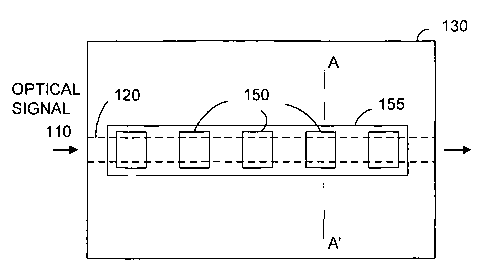
An optical amplifier comprises a device substrate, a first waveguide embedded
in the device substrate, and a plurality of lasers. The lasers are positioned
to provide a first plurality of light beams substantially transverse to the
first waveguide.


French Abstract

L'invention concerne un amplificateur optique qui comprend un substrat de dispositif, un premier guide d'ondes incorporé dans ce substrat de dispositif, et une pluralité de lasers. Ces lasers sont placés de façon à produire une première pluralité de faisceaux lumineux sensiblement transversaux par rapport au premier guide d'ondes.

Claims

Note: Claims are shown in the official language in which they were submitted.


CLAIMS
WHAT IS CLAIMED IS:
I. An optical amplifier comprising:
a device substrate;
a first waveguide embedded in the device substrate; and
a first plurality of lasers positioned to provide a first plurality of light
beams
substantially transverse to the first waveguide.
2. The optical amplifier of claim 1 wherein each of the first plurality of
lasers are
spaced apart from one another along a length of the first waveguide.
3. The optical amplifier of claim 2 wherein the first plurality of lasers are
vertical
cavity surface emitting lasers.
4. The optical amplifier of claim 3 wherein the first plurality of lasers
share a
common substrate.
5. The optical amplifier of claim 4 wherein the vertical cavity surface
emitting lasers
are bonded to the device substrate.
6. The optical amplifier of claim 1 wherein the device substrate is a
phosphate glass
doped with Erbium.
7. The optical amplifier of claim 1 further comprising:
a second waveguide embedded in the device substrate; and
6

a second plurality of lasers positioned to provide a second plurality of light
beams substantially transverse to the second waveguide.
8. The optical amplifier of claim 1, wherein the first plurality of lasers are
evenly
spaced apart from one another.
9. A method of amplifying an optical signal comprising:
directing the optical signal through a waveguide, the optical signal having a
first direction of propagation; and
applying a plurality of light beams substantially transverse to the first
direction
of propagation.
10. The method of claim 9, wherein the plurality of light beams is provided by
a
plurality of laser diodes.
11. The method of claim 10, wherein the optical signal has a wavelength of
approximately 1550 nm, and the plurality of light beams has a wavelength of
approximately 980 nm.
12. The method of claim 11, wherein the applying the plurality of light beams
further comprises:
using a plurality of lasers each using less than 50 mW of power.
13. The method of claim 11, wherein the applying the plurality of light beams
further comprises:
using a plurality of lasers each using less than 20 mW of power.
7

14. The method of claim 9 further comprising:
reflecting the plurality of light beams back at the waveguide after passing
through the waveguide.
15. A method of making an optical signal amplifier comprising:
attaching a plurality of light sources to a surface of a substrate, the
substrate
having a waveguide embedded within, wherein the plurality of light
sources are directed substantially transverse to the waveguide.
16. The method of claim 15, wherein the attaching of the plurality of light
sources
comprises:
bonding a plurality of vertical cavity surface emitting lasers to the surface
of
the substrate.
17. The method of claim 16, wherein each of the plurality of vertical cavity
surface
emitting lasers is spaced apart in a line on a common semiconductor substrate.
18. The method of claim 16, wherein each of the plurality of vertical cavity
surface
emitting lasers is spaced apart by a constant distance.
19. The method of claim 16, wherein the plurality of vertical cavity surface
emitting
lasers each operate at less than 50 mW.
20. The method of claim 16, wherein the plurality of vertical cavity surface
emitting
lasers each operate at less than 20 mW.
8

21. An optical amplifier comprising:
a substrate;
a waveguide embedded within the substrate, the waveguide having a primary
direction of propagation;
an array of lasers positioned to provide a plurality of pumped light beams
transverse to the primary direction of propagation.
22. The optical amplifier of claim 21, wherein at least one of the array of
lasers
operates at less than 20 mW of power.

Description

Note: Descriptions are shown in the official language in which they were submitted.


CA 02469824 2004-06-07
WO 03/052885 PCT/US02/37677
OPTICAL AMPLIFIER WITH TRANSVERSE PUMP
1. Field
The described invention relates to the field of optical signal amplification.
In
particular, the invention relates to amplifying an optical signal using
transverse pumping
light beams.
2. Back rg ound
A waveguide may serve as an optical amplifier by doping it with ions of a rare
earth element such as Erbium. An optical signal propagating in the waveguide
is
amplified when a pumping light beam is introduced. For example, Erbium ions,
excited to
a higher energy state with a pumping light beam having a wavelength of
approximately
980 nm or 1480 nm, will amplify an optical signal in a wide wavelength band
around
1530-1600 nm as the Erbium ions fall down to a lower energy state. This
technique is
well-known in optical fiber amplification.
Figure 1 is a schematic diagram showing one prior art method of amplifying an
optical signal 10 in a planar waveguide 20. The waveguide 20 is embedded in a
substrate
30 and doped with Erbium ions. An optical signal 10 is directed into the
waveguide 20
and propagates through the waveguide 20. A laser 50 supplies pumping light
beams into
the waveguide 20 in a co-propagating direction, i.e., in substantially the
same direction as
the optical signal propagates. The signal 10 and the pump 50 are combined to
the same
waveguide 20, for example, in an evanescent directional coupler. In one
example, an
optical signal 10 having wavelength of approximately 1550 nm is amplified as
laser 50
supplies pumping light beams of approximately 980 nm or 1480 nm wavelength.
Figure 2 is a schematic diagram showing another prior art method of amplifying
an
optical signal. In Figure 2, a pump laser 50 is directed from the opposite end
of the
waveguide 20 to pump light in a counter-propagating direction, i.e., in a
direction opposite

CA 02469824 2004-06-07
WO 03/052885 PCT/US02/37677 ..
to that of the optical signal. Similar to Figure l, the optical signal is
amplified within the
waveguide 20 and then exits the substrate 30.
Modern optical networks use single-mode optical fibers for transmission over
long
distances. This avoids signal degradation coming from chromatic dispersion,
i.e.
dependence of the speed of the light on its wavelength. For efficient
interfacing with
single mode fibers, all optical components, including fiber or waveguide
amplifiers, are
effectively single-mode. Due to a general principle of optics, "brightness
conservation
theorem", power of light in a single mode cannot be increased using. just
linear passive
(not adding energy) optical elements. This results in a fact that the power of
light with a
certain wavelength from only one mode can be coupled to a single mode
waveguide. For
amplifiers, it translates that only one pump laser with a certain wavelength
can supply
pump light in each direction of propagation and each polarization.
The optical signal experiences gain in an optical amplifier provided that the
intensity of the pump is higher than a certain threshold value dependent on
the intensity of
1 S the optical signal and material properties of the optical amplifier. In
order to achieve high
enough gain, the intensity of the pump must be much higher than the threshold
value.
Consequently, a high power of a pump laser is typically required.
There are several disadvantages of the above methods compared to the invention
described below. First, the relatively high power laser used in the described
co-
propagating and counter-propagating amplification is expensive. Second, high
power
lasers have a high power dissipation, which may cause thermal issues in their
packaging.
Third, the reliability of high power lasers is generally not as good as that
of lower power
lasers.
BRIEF DESCRIPTION OF THE DRAWINGS
Figure 1 is a schematic diagram showing one prior art method of amplifying an
optical signal in a planar waveguide.

CA 02469824 2004-06-07
WO 03/052885 PCT/US02/37677 .
Figure 2 is a schematic diagram showing another prior art method of amplifying
an
optical signal.
Figure 3 is a schematic diagram showing a top view of one embodiment of an
optical amplifier.
Figure 4 is a schematic diagram showing a cross sectional view of an optical
amplifier taken along line A-A' of Figure 3.
Figure 5 is a graph showing an example of increase in optical signal power
based
on optical pumping.
DETAILED DESCRIPTION
An apparatus and method for amplifying an optical signal in a waveguide is
disclosed. In one embodiment, multiple lower power lasers are interspersed
along a length
of the waveguide to provide pumping light beams transverse to the direction of
propagation of the optical signal.
Figure 3 is a schematic diagram showing a top view of one embodiment of an
optical amplifier. An optical signal 110 enters into and propagates through
waveguide
120, which is embedded in a substrate 130. There are various ways to fabricate
a
waveguide embedded in a substrate, such as by diffusion of various ionic
species, etching,
and epitaxial growth. "Embedded within a substrate" is meant to include these
various
ways, including silicon-on-insulator. In some cases, the waveguide may
actually be
deposited on top of a substrate and covered with a cladding material different
from the
substrate, but is also meant to be covered by the term "embedded within a
substrate".
In one embodiment, waveguide 120 is a single-mode waveguide. A plurality of
light sources 150, such as laser diodes, are coupled to the substrate 130 to
direct the
pumping light beams substantially transverse to the embedded waveguide 120.
In one embodiment, the light sources 150 are spaced evenly apart along the
length
of the embedded waveguide 120. However, other embodiments may include
different
spacings between light sources 150. In one embodiment, the light sources 150
comprise
3

CA 02469824 2004-06-07
WO 03/052885 PCT/US02/37677
vertical cavity surface emitting lasers (VCSELs). The VCSELS may be fabricated
from a
common semiconductor substrate 155 and may be bonded to a surface of the
device
substrate 130. This allows lithographically-defined spacing between the
VCSELs.
In one embodiment, the VCSELs use relatively low power. For example, a
VCSEL may emit, but is not limited to, less than 20 mW of power. Comparable
high
power lasers used in co-propagating and counter-propagating architectures use
higher
power lasers, such as, but not limited to, 100 mW.
Figure 4 is a schematic diagram showing a cross sectional view of an optical
amplifier taken along line A-A' of Figure 3. In one embodiment, after the
pumping light
beam 160 from the light source 150 passes through the waveguide 120, the
pumping light
beam is reflected off a lower surface 180 and sent back to the waveguide 120,
as shown by
arrows 170. In one embodiment, the reflection at lower surface 180 is due to a
change in
refractive index, which may be achieved by the lower surface 180 adjoining
either a
different material, or the same material but having different properties, as
is well-known.
In one embodiment, the lower surface 180 is adjoining to air or to a heatsink.
In one embodiment, the spacing between the light source 150 and the embedded
waveguide 120 is relatively small, e.g., 5 microns. In another embodiment, a
lens or
collimator may be coupled between the light sources and the substrate.
Figure 5 is an example graph illustrating an increase in optical signal power
based
on the optical pumping. In one embodiment, the pumping light beams have a
power Pp~MP
that is applied to the optical signal 200. The pump power Pp~Mp 202 is
greatest directly
under a light source 210. As the optical signal 200 propagates through the
waveguide, it is
successively pumped by multiple light sources 210.
In one embodiment, multiple waveguides may be embedded in the same substrate.
Each waveguide may have a set of transverse pumps for amplifying an optical
signal
within the waveguide. In one embodiment, the transverse pumps are VCSELs. A
matrix
of VCSELs fabricated on a common substrate may be used to amplify optical
signals in
multiple waveguides.

CA 02469824 2004-06-07
WO 03/052885 PCT/US02/37677
Thus, an apparatus and method for amplifying an optical signal is disclosed.
However, the specific arrangements and methods described herein are merely
illustrative.
For example, there are various ways to fabricate a waveguide embedded in a
substrate,
such as by diffusion of various ionic species, etching, and epitaxial growth.
One skilled in
the art could use any of various methods to fabricate such an embedded
waveguide.
Numerous modifications in form and detail may be made without departing from
the scope
of the invention as claimed below. The invention is limited only by the scope
of the
appended claims.

Representative Drawing
A single figure which represents the drawing illustrating the invention.
Administrative Status

2024-08-01:As part of the Next Generation Patents (NGP) transition, the Canadian Patents Database (CPD) now contains a more detailed Event History, which replicates the Event Log of our new back-office solution.

Please note that "Inactive:" events refers to events no longer in use in our new back-office solution.

For a clearer understanding of the status of the application/patent presented on this page, the site Disclaimer , as well as the definitions for Patent , Event History , Maintenance Fee  and Payment History  should be consulted.

Event History

Description Date
Time Limit for Reversal Expired 2011-11-22
Application Not Reinstated by Deadline 2011-11-22
Inactive: Abandoned - No reply to s.30(2) Rules requisition 2011-02-02
Deemed Abandoned - Failure to Respond to Maintenance Fee Notice 2010-11-22
Inactive: S.30(2) Rules - Examiner requisition 2010-08-02
Amendment Received - Voluntary Amendment 2010-05-20
Amendment Received - Voluntary Amendment 2009-12-21
Inactive: S.30(2) Rules - Examiner requisition 2009-06-19
Inactive: IPRP received 2007-03-23
Inactive: IPC from MCD 2006-03-12
Inactive: Cover page published 2004-08-17
Letter Sent 2004-08-10
Inactive: Acknowledgment of national entry - RFE 2004-08-10
Application Received - PCT 2004-07-09
National Entry Requirements Determined Compliant 2004-06-07
Request for Examination Requirements Determined Compliant 2004-06-07
All Requirements for Examination Determined Compliant 2004-06-07
National Entry Requirements Determined Compliant 2004-06-07
Application Published (Open to Public Inspection) 2003-06-26

Abandonment History

Abandonment Date Reason Reinstatement Date
2010-11-22

Maintenance Fee

The last payment was received on 2009-11-03

Note : If the full payment has not been received on or before the date indicated, a further fee may be required which may be one of the following

  • the reinstatement fee;
  • the late payment fee; or
  • additional fee to reverse deemed expiry.

Patent fees are adjusted on the 1st of January every year. The amounts above are the current amounts if received by December 31 of the current year.
Please refer to the CIPO Patent Fees web page to see all current fee amounts.

Fee History

Fee Type Anniversary Year Due Date Paid Date
Basic national fee - standard 2004-06-07
MF (application, 2nd anniv.) - standard 02 2004-11-22 2004-06-07
Registration of a document 2004-06-07
Request for examination - standard 2004-06-07
MF (application, 3rd anniv.) - standard 03 2005-11-22 2005-11-04
MF (application, 4th anniv.) - standard 04 2006-11-22 2006-11-02
MF (application, 5th anniv.) - standard 05 2007-11-22 2007-11-05
MF (application, 6th anniv.) - standard 06 2008-11-24 2008-11-07
MF (application, 7th anniv.) - standard 07 2009-11-23 2009-11-03
Owners on Record

Note: Records showing the ownership history in alphabetical order.

Current Owners on Record
INTEL CORPORATION
Past Owners on Record
ANDREW ALDUINO
CHRISTOPHER SCHOLZ
RONGCHUNG TYAN
Past Owners that do not appear in the "Owners on Record" listing will appear in other documentation within the application.
Documents

To view selected files, please enter reCAPTCHA code :


To view images, click a link in the Document Description column. To download the documents, select one or more checkboxes in the first column and then click the "Download Selected in PDF format (Zip Archive)" or the "Download Selected as Single PDF" button.

List of published and non-published patent-specific documents on the CPD .

If you have any difficulty accessing content, you can call the Client Service Centre at 1-866-997-1936 or send them an e-mail at CIPO Client Service Centre.


Document
Description 
Date
(yyyy-mm-dd) 
Number of pages   Size of Image (KB) 
Description 2004-06-06 5 187
Abstract 2004-06-06 1 53
Drawings 2004-06-06 3 24
Claims 2004-06-06 4 82
Representative drawing 2004-08-15 1 4
Description 2009-12-20 6 225
Claims 2009-12-20 3 82
Acknowledgement of Request for Examination 2004-08-09 1 177
Notice of National Entry 2004-08-09 1 202
Courtesy - Certificate of registration (related document(s)) 2004-08-09 1 105
Courtesy - Abandonment Letter (Maintenance Fee) 2011-01-16 1 172
Courtesy - Abandonment Letter (R30(2)) 2011-04-26 1 165
PCT 2004-06-06 4 122
Fees 2005-11-03 1 33
Fees 2006-11-01 1 43
PCT 2007-03-22 3 162
Fees 2007-11-04 1 50
Fees 2008-11-06 1 53
Fees 2009-11-02 1 49