Note: Descriptions are shown in the official language in which they were submitted.
CA 02470206 2008-11-03
CH92001003 8
-1-
ELECTRODE STRUCTURE FOR
ELECTRONIC AND OPTO-ELECTRONIC DEVICES
TECHNICAL FIELD
The present invention is related to an electrode design for an electronic
device. More
particularly the invention relates to an electrode modification for electronic
and
opto-electronic devices.
BACKGROUND OF THE INVENTION
Electronic and opto-electronic devices such as organic light-emitting diodes
(OLEDs) are
known in the art. Those OLEDs are also referred to as organic
electroluminescent (EL)
devices which generally comprise an organic electroluminescent material
sandwiched between
two electrodes. Generally, the organic electroluminescent material is a
multilayer structure
comprising an electron transport layer, an electroluminescent layer and a hole
transport layer.
Upon application of an electrical current, the material radiates light
generated by
recombination of electrons and holes in the organic material. However, the
organic
luminescent materials are sensitive to impurities, oxygen, and humidity.
Further, in some
electronic or opto-electronic devices, the electrodes influence the intensity,
stability, and
reliability of the device. Organic electroluminescent devices (materials and
structure) are
known in thf" art as, for example, disclosed in US patent 4,356,429, US patent
5,593,788, or
US patent 5,408,109.
With multilayer device architectures now well understood and widely used, a
remaining
performance limitation of OLEDs is the electrode. The main figure of merit for
electrode
materials is the position of the electrode Fermi energy relative to the
relevant organic
molecular energy levels. in some applications it is also desirable for an
electrode to assist light
extraction. Electrodes should also be chemically inert-with respect to the
adjacent organic
material to provide long term stability of the electroluminescent device.
CA 02470206 2004-06-10
WO 03/055275 PCT/IB02/04975
-2-
Much attention has been paid to the cathode, largely because good electron
injectors are low
work function metals which are also chemically reactive and oxidize quickly in
atmosphere,
limiting the OLED reliability and lifetime. Much less attention has been paid
to the
optimization of the anode contact, since conventional ITO anodes generally
outperform the
cathode contact leading to an excess of holes. Due to this excess, and the
convenience
associated with the conductivity and transparency of indium-tin-oxide (ITO),
improved
anodes have not been as actively sought as improved cathodes.
Problems concerning sufficient hole injection and operational stability arose
with the use of
organic electroluminescent devices. Some problems have been relieved by a
fluorocarbon
treatment of the device's anode. US patent 6,127,004 relates to a method of
forming an
electroluminescent device comprising the steps of providing a substrate having
a top surface
coating with a material including an anode having indium-tin-oxide (ITO); and
forming an
amorphous conductive layer over the anode by providing a fluorocarbon gas in a
radical
source cavity and subjecting such fluorocarbon gas to a reduced pressure in a
range of 0.1 to
20 mT. Further an RF field is applied across the fluorocarbon gas in the
radical source cavity
to form a plasma having CFx radicals and the CFx radicals are deposited onto
the anode
forming an amorphous CFx conductive polymer layer on the anode. Then a
plurality of layers
over the amorphous CFx conductive polymer layer with such layers including at
least one
organic electroluminescent layer and a cathode over the electroluminescent
layer are formed.
US patent 6,208,075 relates also to an organic electroluminescent device which
has a
conductive fluorocarbon polymer layer disposed over an anode and US patent
6,208,077
shows a thin non-conductive fluorocarbon polymer layer disposed over the
anode. The
mentioned fluorocarbon polymer layers are applied because of their transport
properties and
serve therefore as hole injection layers. The fluorocarbon polymer layers
adheres preferably on
anodes containing oxygen, e.g. ITO, otherwise using other materials lead to
unstable device
performance.
The international application with international publication number WO
99/39393, presently
assigned to the assignee of the instant application, relates to an organic
light emitting device
having in order an anode, a barrier layer, an anode modification layer, an
organic region, and a
CA 02470206 2004-06-10
WO 03/055275 PCT/IB02/04975
-3-
cathode. The anode modification layer is in direct contact with the organic
region. The barrier
layer is arranged to separate the anode modification layer form the anode but
however this
layer interferes the injection as it shows barrier properties.
An opto-electronic device can work either as a top emission device or a bottom
emission
device, also referred to as back emission device. For bottom emission devices,
the anode
should be nearly transparent such that the emitted light can pass through the
anode.
Indium-tin-oxide (ITO) has been widely applied as anode because it forms
nearly transparent
layers. ITO has the disadvantage that it can partly react with the layer on
top, e.g. the hole
transporting organic material. This can lead to a shortening of the lifetime
of the device. To
circumvent the shortening, usually a buffer layer, e.g. CuPc, is used between
the anode and the
organic material, but on the other hand the buffer layer has a high resistance
and interferes the
injection. The use of a fluorocarbon polymer layer, as mentioned above, allows
to discard the
buffer layer.
For top emission devices molybdenum or platinum have been applied. These
materials are not
transparent and have a strong optical absorption. The reflection index of
platinum is not
optimal. Silver (Ag) and aluminum (Al) have a high reflectivity but a lower
work function and
are therefore unsuitable as anode materials. In general, materials having a
high work function
are rendered to be best suited as anode material. Low work function materials,
e.g. Al,
generally are highly chemical active even when covered with a buffer layer,
e.g. CuPc, and
consequently those materials are therefore unsuitable to form an anode.
Moreover, also the
combination of such a material and the fluorocarbon polymer layer leads to
unreliable
performance and therefore to useless devices.
From the above follows that there is still a need in the art for improved
structures of electrodes
in electronic and opto-electronic devices which show long term stability and
high efficiency.
It is therefore an object of the present invention to provide an improved
electrode structure for
electronic devices comprising an organic material and displays based thereon.
CA 02470206 2004-06-10
WO 03/055275 PCT/IB02/04975
-4-
SUMMARY AND ADVANTAGES OF THE INVENTION
In accordance with the present invention, there is provided an electronic
device comprising a
first electrode substantially having a conductive layer, a nonmetal layer
formed on the
conductive layer, a fluorocarbon layer formed on the nonmetal layer, a
structure formed on the
fluorocarbon layer, and a second electrode formed on the structure.
The electronic device can further comprise a buffer layer between the
conductive layer and the
nonmetal layer. Such a buffer layer reduces advantageously the reactions
between the first
electrode and further layers. In particular oxidation processes can be
avoided.
In a preferred embodiment, the conductive layer comprises aluminum (Al).
Aluminum is
normally highly reflective but also reactive. However, having the nonmetal
layer or the
mentioned buffer layer in combination with the nonmetal layer on top of the
conductive layer
than it turns out that electroluminescent devices with excellent properties
and characteristics
can be designed.
The nonmetal layer can comprise an oxide. Oxides are plentifully available or
can be formed
from many materials or compounds. The oxide can be based on a material
selected from one
of the groups: 3d transition metal group, IIIA group, IVA group, rare earth
metal group, or a
combination thereof.
When the nonmetal layer is an oxide different from a potential oxide that can
be formed by
the conductive layer, also referred to as foreign oxide, then the advantage
occurs that electrical
and optical properties, e.g. injection and transparency, of the electrode can
be tailored. For
example, when the conductive layer is formed from Al then the potential oxide
that can be
formed or created by the conductive layer is aluminum oxide. It is a fact that
aluminum oxide
has a higher resistance than, e.g., nickel oxide (NiOX). Thus using NiOX as
the foreign oxide to
form the nonmetal layer shows better hole injection properties than aluminum
oxide. The
combination of the conductive layer having a high reflectivity and the
nonmetal layer
supporting hole injection additionally leads to reliable and significantly
improved
electroluminescent devices with improved light output.
CA 02470206 2004-06-10
WO 03/055275 PCT/IB02/04975
-5-
Depending on the nature of the conductive layer it is advantageous if the
nonmetal layer has a
thickness in the range of one monolayer to 20 nm, because then the electronic
device shows
excellent long term stability and high efficiency. In electroluminescent
devices (OLEDs), e.g.,
active driven devices, higher values of thickness are often associated with
higher driving
voltages.
The conductive layer can comprises a metal, a semiconductor, or an organic
conductor.
Moreover, the conductive layer can comprise an optical reflective material.
Preferred
materials for the conductive layer, i.e. for the electrode, is aluminum (Al)
or silver (Ag).
Those materials come into focus when an oxide or foreign oxide is used as
nonmetal layer on
the conductive layer.
The conductive layer can form a mirror-like surface. That means the anode
works as a mirror
and reflects the emitted light to intensify the light output. This concept
works for top as well
as bottom emitting devices.
Under the term opto-electronic device is understood any device that works as
an
electrical-to-optical or optical-to-electrical transducer, or an instrument
that uses such a device
in its operation.
The electronic device can comprise a substrate that is in contact with the
conductive layer or
the structure. The substrate can be any material including glass, i.e. a
transparent material for
top emission devices; Si, or plastic, i.e. an opaque material for bottom
devices. The substrate
can be used as a basis for forming an electronic device.
The electronic device can be part of an electroluminescent device, a
transistor, or a sensor.
This shows that the electrode design can be broadly used. The structure is
however not limited
to the mentioned applications. It is also not limited to the use with organic
structures, but it
can be used in connection with the following structures: organic/inorganic,
organic-inorganic
hybrid, or inorganic. Moreover, the electrode design with the structure is
applicable in a broad
variety of electronic and opto-electronic applications.
CA 02470206 2004-06-10
WO 03/055275 PCT/IB02/04975
-6-
The present invention also relates to a method for forming the electronic
device. The method
comprising the steps of: providing a conductive layer to serve as a first
electrode; forming a
nonmetal layer on the first electrode, depositing a fluorocarbon layer onto
the nonmetal layer,
forming a plurality of layers as structure on the fluorocarbon layer, and
forming a second
electrode on the structure.
CA 02470206 2009-11-16
CH920010038 7
DESCRIPTION OF THE DRAWINGS
Preferred embodiments of the invention are described in detail below, by way
of example only,
with reference to the following schematic drawings.
FIG. 1 shows a schematic illustration of an organic electroluminescent device
of the
prior art.
FIG. 2a shows a schematic illustration of a first embodiment of an organic
electroluminescent device.
FIG. 2b shows a schematic illustration of a second embodiment of an organic
electroluminescent device.
FIG. 3a shows a schematic illustration of an example of an organic transistor.
FIG. 3b shows a schematic illustration of an example of an organic transistor.
FIG. 4 shows a diagram displaying the current-voltage relationship of a first
tested
electroluminescent device and the current-voltage and brightness-voltage
relationship of second tested electroluminescent device.
FIG. 5 shows a diagram displaying the current-voltage and brightness-voltage
relationship of a third tested electroluminescent devices.
FIG. 6 shows a diagram displaying the efficiency-voltage relationship of the
second
tested electroluminescent device.
FIG. 7 shows a standardized diagram of the lifetime of a fourth tested
electroluminescent device.
The drawings are provided for illustrative purpose only and do not necessarily
represent
practical examples of the present invention to scale.
CA 02470206 2004-06-10
WO 03/055275 PCT/IB02/04975
-8-
DETAILED DESCRIPTION OF THE INVENTION
Although the present invention is applicable in a broad variety of electronic
and
opto-electronic applications it will be described with the focus put on an
application to an
organic electroluminescent device, i.e. an organic light-emitting diode
(OLED), and an
organic transistor.
Before embodiments of the present invention are described, the configuration
of a prior art
electroluminescent device is addressed.
Fig 1 shows an organic electroluminescent device 100 that has a substrate 102,
on which is
disposed an indium-tin-oxide (ITO) anode 104. The substrate 102 and the ITO
anode 104 are
light transparent. A polymer layer 108 is arranged in direct contact with the
ITO anode 104.
An organic light-emitting structure 110 is formed between the ITO anode 104
that is coated
with the polymer layer 108 and a cathode 120. The organic light-emitting
structure 110 is
comprised of, in sequence, an organic hole-transporting layer 112, an organic
light-emitting
layer 114, and an organic electron-transporting layer 116. When an electrical
potential
difference is applied between the anode 104 and the cathode 120 such that the
anode 104 is
electrically positive relative to the cathode 120, the cathode 120 will inject
electrons into the
electron-transporting layer 116, and the electrons will traverse the electron-
transporting layer
116 and the light-emitting layer 114. At the same time, holes will be injected
from the anode
104 into the hole-transporting layer 112, and the holes will migrate across
layer 112, and
eventually recombine with electrons near the interface between the hole-
transporting layer 112
and the light-emitting layer 114. When electrons from the conduction band
recombine
radiatively with holes from the valence band, photons can be emitted through
the
light-transmissive anode 104 and substrate 102, as indicated by the arrows,
for viewing by an
observer.
The polymer layer 108 can be prepared by plasma polymerization of a
fluorocarbon gas in a
RF plasma. The fluorocarbon polymer is a teflon-like polymer and is
substantially formed of
carbon and fluorine. It may also contain hydrogen and/or a small amount of
impurities such as
nitrogen, oxygen, etc. The thickness of the polymer layer is so selected that
it would have a
CA 02470206 2004-06-10
WO 03/055275 PCT/IB02/04975
-9-
full coverage on the underlying conductive layer, and that its low
conductivity has no negative
impacts on device performance.
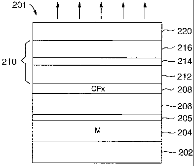
Fig. 2a shows a schematic illustration of a first embodiment of an organic
electroluminescent
device 200. The organic electroluminescent device 200, that here is a top
emission device, has
a substrate 202, on which is disposed a first electrode 204, also referred to
as anode 204. The
anode 204 comprises a layer of conductive and highly reflective material,
labeled with M, so
as to provide a mirror-like surface. A nonmetal layer 206 comprising
substantially an oxide is
formed on the anode 204. Moreover, on the nonmetal layer 206 a polymer layer
208
substantially comprising fluorocarbon is formed. An organic light-emitting
structure 210 is
formed between the nonmetal layer 206 that is coated with the fluorocarbon
layer 208 and a
cathode 220. The organic light-emitting structure 210 is comprised of, in
sequence, an organic
hole-transporting layer 212, an organic light-emitting layer 214, and an
organic
electron-transporting layer 216. The described structure is distinctive over
the prior art as
shown with reference to Fig. 1. The nonmetal layer 206 is arranged between the
anode 204
and the polymer layer 208.
The polymer layer 208 is prepared by plasma polymerization of a fluorocarbon
gas in a RF
plasma. Also possible is to apply chemical vapor deposition (CVD).
The anode 204 comprises a layer of conductive and highly reflective material,
preferably Al or
Ag, so as to provide a mirror-like surface. The nonmetal layer 206 comprises
an oxide that
here is different form the oxide that the conductive and highly reflective
material forms if it
comes into contact with oxygen or under ambient, e.g. ITO, NiOX. Several
methods of
deposition of the nonmetal layer 206 are listed below:
- chemical vapor deposition (CVD), including plasma-enhanced chemical vapor
deposition
(PECVD);
- sputter deposition or reactive (e.g. in an oxygen environment) sputter
deposition;
- thermal evaporation;
- electron-beam evaporation;
- oxygen plasma (plasma-assisted oxidation);
- thermal annealing in an oxidizing environment;
- UV-ozone treatment;
- wet-chemical oxidation;
- electrochemical oxidation.
CA 02470206 2004-06-10
WO 03/055275 PCT/IB02/04975
-10-
The substrate 202 is used as a basis and should be electrically insulated. As
the presented
device is a top emission device, i.e. the generated light is reflected at the
mirror-like surface of
the anode 204 and transmitted through the cathode 220, as indicated by the
arrows, the
substrate can be opaque. In that case the cathode 220 should be light-
transmissive.
The present invention is not restricted to top emission devices and can of
course be applied to
bottom emission devices as well with all its advantages. Then the anode 204
should have
transmissive characteristics.
When a bottom emission device or architecture is desired, then the anode 204
as well as the
substrate 202 should be light-transmissive. In that case the anode 204
suitably comprises
semi-transparent materials or metal films. These can comprise a transparent
conducting oxide,
such as indium-tin-oxide, doped tin oxide, or aluminum doped zinc oxide. These
materials
should be suitably deposited on the transparent substrate 202 such as glass
quartz or a polymer
substrate, e.g. polyethylene terephthalate or polyvinyl acetate.
A variety of compositions for the organic light-emitting structure 210 can be
utilized.
Hole transport layers and Hole injection layers: The following materials are
suited as hole
injection layer and organic hole-transporting layer 212. Materials containing
aromatic amino
groups, like tetraphenyldiaminodiphenyl (TPD-1, TPD-2, or TAD) and NPB (see C.
Tang,
SIID Meeting San Diego, 1996, and C. Adachi et al. Applied Physics Letters,
Vol. 66, p. 2679,
1995), TPA, NIPC, TPM, DEH (for the abbreviations see for example: P.
Borsenberger and
D.S. Weiss, Organic Photoreceptors for Imaging Systems, Marcel Dekker, 1993).
These
aromatic amino groups can also be incorporated in polymers, starburst (for
example: TCTA,
m-MTDATA, see Y. Kuwabara et al., Advanced Materials, 6, p. 677, 1994, Y.
Shirota et al.,
Applied Physics Letters, Vol. 65, p. 807, 1994) and spiro compounds.
Further examples are: Copper(II) phthalocyanine (CuPc),
(N,N'-diphenyl-N,N'-bis-(4-phenylphenyl)-1,1'-biphenyl-4,4'-diamine), distyryl
arylene
derivatives (DSA), naphthalene, naphthostyrylamine derivatives (e.g. NSD),
quinacridone
(QA), poly(3-methylthiophene) (P3MT) and its derivatives, perylene and
perylene derivatives,
polythiophene (PT), 3,4,9,10-perylenetetracarboxylic dianhydride (PTCDA), PPV
and some
CA 02470206 2004-06-10
WO 03/055275 PCT/IB02/04975
-11-
PPV derivatives, for example MEH-PPV, poly(9-vinylcarbazole) (PVK), discotic
liquid
crystal materials (HPT).
Electron transport/Emitting materials are: Alq3, Gaq3, Inq3, Scq3, (q refers
to
8-hydroxyquinolate or it's derivatives) and other 8-hydroxyquinoline metal
complexes such as
Znq2, Beq2, Mgq2, ZnMq2, BeMq2, BAlq, and AlPrq3, for example. These materials
can be
used as the organic electron-transporting layer 216 or organic light-emitting
layer 214.
Other classes of electron transporting materials are electron-deficient
nitrogen-containing
systems, for example oxadiazoles like PBD (and many derivatives), and
triazoles, for example
TAZ (1,2,4-triazole).
These functional groups can also be incorporated in polymers, starburst and
spiro compounds.
Further classes are materials containing pyridine, pyrimidine, pyrazine and
pyridazine
functionalities.
Finally, materials containing quinoline, quinoxaline, cinnoline, phthalazine
and quinaziline
functionalities are well known for their electron transport capabilities.
Other materials are didecyl sexithiophene (DPS6T), bis-triisopropylsilyl
sexithiophene
(2D6T), azomethin-zinc complexes, pyrazine (e.g. BNVP), styrylanthracene
derivatives (e.g.
BSA-1, BSA-2), non-planar distyrylarylene derivatives, for example DPVBi (see
C.
Hosokawa and T. Kusumoto, International Symposium on Inorganic and Organic
Electroluminescence 1994, Hamamatsu, 42), cyano-substituted polymers such as
cyano-PPV
(PPV means poly(p-phenylenevinylene)) and cyano-PPV derivatives.
The following materials are particularly well suited as
Emission layers and Dopants: Anthracene, pyridine derivatives (e.g. ATP),
Azomethin-zinc
complexes, pyrazine (e.g. BNVP), styrylanthracene derivatives (e.g. BSA-1, BSA-
2),
Coronene, Coumarin, DCM compounds (DCMl, DCM2), distyryl arylene derivatives
(DSA),
alkyl-substituted distyrylbenzene derivatives (DSB), benzimidazole derivatives
(e.g. NBI),
naphthostyrylamine derivatives (e.g. NSD), oxadiazole derivatives (e.g. OXD,
OXD-1,
OXD-7), N,N,N',N'-tetrakis(m-methylphenyl)-1,3-diaminobenzene (PDA), perylene
and
CA 02470206 2004-06-10
WO 03/055275 PCT/IB02/04975
-12-
perylene derivatives, phenyl-substituted cyclopentadiene derivatives, 12-
phthaloperinone
sexithiophene (6T), polythiophenes, quinacridones (QA) (see T. Wakimoto et
al.,
International Symposium on Inorganic and Organic Electroluminescence, 1994,
Hamamatsu,
77), and substituted quinacridones (MQA), rubrene, DCJT (see for exainple: C.
Tang, SID
Conference San Diego; Proceedings, 1996, 181), conjugated and non-conjugated
polymers,
for example PPV and PPV derivatives, dialkoxy and dialkyl PPV derivatives, for
example
MEH-PPV (poly(2-methoxy)-5-(2'-ethylhexoxy)- 1,4-phenylene-vinylene),
poly(2,4-bis(cholestanoxyl)-1,4-phenylene-vinylene) (BCHA-PPV), and segmented
PPVs (see
for example: E. Staring in International Symposium on Inorganic and Organic
Electroluminescence, 1994, Hamamatsu, 48, and T. Oshino et al. in Sumitomo
Chemicals,
1995 monthly report).
There are many other organic materials known as being good light emitters,
charge transport
materials, and charge injection materials, and many more will be discovered.
These materials
can be used as well for making light-emitting structures.
The organic hole-transporting layer 212 comprises at least one hole
transporting aromatic
tertiary amine, where the latter is understood to be a compound containing at
least one
trivalent nitrogen atom that is bonded only to carbon atoms, at least one of
which is a member
of an aromatic ring. In one form the aromatic tertiary amine can be an
arylamine, such as a
monarylamine, diarylamine, triarylamine, or a polymeric arylamine.
The organic light-emitting layer 214 comprises of a luminescent or fluorescent
material or
material combination (host and dopant(s)), where electroluminescence is
produced as a result
of electron-hole pair recombination in this region. In the simplest
construction, the
luminescent layer comprises of a single component, that is a pure material
with a high
fluorescent efficiency. A well known material is tris (8-quinolinato)
aluminum, (Alq).
The cathode electrode 220 comprises a metal or electrode configuration with a
low work
function (e.g., less than 4.0 eV, preferably less than 3.5 eV) selected from
alkali metals,
alkaline earth metal or rare earth metal, combined compounds, such as LiF/Al,
LiZ0/Al, or
alloys thereof. Preferred metals are calcium or alloys such as
magnesium/silver;
CA 02470206 2009-11-16
CH920010038 13
lithium/aluminum; or magnesium/aluminum. These cathode configurations provide
low work
function and thus enhanced quantum efficiency for the device.
The same reference numbers are used to denote the same or like parts.
Fig. 2b shows a schematic illustration of a second embodiment of an organic
electroluminescent
device 201. The organic electroluminescent device 201, has the substrate 202,
on which is
disposed the anode 204. The nonmetal layer 206 is formed on the anode 204.
Between the
nonmetal layer 206 and the anode 204 is formed a buffer layer 205. Suitable
buffer layer
materials are Ti, Ni, Pt, or ITO. The buffer layer 205 should be a thin layer
with a thickness of a
few Angstrom to several nanometers. This buffer layer 205 reduces the chemical
reactions and
avoids interdiffusion between the conductive and highly reflective layer of
the anode 204 and
other layers. In particular oxidation and interdiffusion processes can be
avoided. The organic
light-emitting structure 210 is formed between the nonmetal layer 206 and the
cathode 220 as
described above.
Fig. 3a shows a schematic illustration of an example of an organic transistor
300. The organic
transistor 300 comprises a substrate 302, a gate layer 330 being a metal, a
gate dielectric layer
340, e.g. SiO, and an organic structure 310. Further, the organic transistor
300 comprises as the
known connectors a source electrode 320 and a drain electrode 311 which are
arranged on the
organic structure 3 10. Moreover, the source electrode 320 comprises a
conductive layer 304, a
nonmetal layer 306, and a polymer layer 308, which is in direct contact with
the organic
structure 3 10. In another example, the drain electrode 311 comprises the
conductive layer 304,
the nonmetal layer 306, and the polyiner layer 308 (not shown). The drain
electrode 311 and the
source electrode 320 can also have the same structure.
Fig. 3b shows a schematic illustration of an example of a further organic
transistor 301. The
same reference numbers are used to denote the same or like parts. The further
organic transistor
301 comprises the substrate 302, the gate layer 330, the gate dielectric layer
340, and the
organic structure 310. The difference to Fig. 3a is that the source electrode
320 and the drain
electrode 311 are buried in the organic structure 310. The conductive layer
304,
CA 02470206 2004-06-10
WO 03/055275 PCT/IB02/04975
- 14-
the nonmetal layer 306, and the polymer layer 308 are connected to the gate
dielectric layer
340.
Fig. 4 shows a diagram displaying the current-voltage relationship of a first
tested
electroluminescent device, labeled with I, and the current-voltage (thick
curve) and
brightness-voltage (thin curve) relationship of second tested
electroluminescent device,
labeled with II, according to the present invention. The second tested
electroluminescent
device is structured as follows: anode arrangement AUA12O3/CFX(3nm); organic
light-emitting
structure: NPB(45nm)/Alq3(65nm); cathode Ca(15nm). The second tested
electroluminescent
device shows a much better performance, especially in brightness, than the
first tested
electroluminescent device having a known configuration.
Fig. 5 shows a diagram displaying the current-voltage (thick curve) and
brightness-voltage
(thin curve) characteristic of a third tested electroluminescent device having
the following
structure: anode arrangement Al/Ni/NiOX/CFX(4nm); organic light-emitting
structure: NPB(50
nm)/Alq3(50nm); cathode Ca(15nm). The third tested electroluminescent device
having the
buffer layer comprising Ni and the nonmetal layer comprising NiOX shows even
steeper
characteristics compared to Fig. 4 indicating an excellent performance of the
third tested
electroluminescent device.
Fig. 6 shows a diagram displaying the efficiency-voltage relationship of the
second tested
electroluminescent device. The graph indicates that the second tested
electroluminescent
device is best suited for OLEDs.
Fig. 7 shows a standardized diagram of the lifetime of a fourth tested
electroluminescent
device. The fourth tested electroluminescent device is structured as follows:
anode
arrangement Al/Al2O3/CFX(10nm); organic light-emitting structure: CuPu(lOnm
)/NPB(45nm)/A1q3(65nm); cathode Ca(3nm)/Ag(15nm). The extrapolated lifetime,
i.e. the
time until the device shows half the brightness compared to the initial
brightness under
constant current conditions, is about 28 years, which speaks for a highly
reliable
electroluminescent device. The initial brightness was 88 Cd/m2.
CA 02470206 2004-06-10
WO 03/055275 PCT/IB02/04975
-15-
EXAMPLE
The following example is presented for further understanding. For purposes of
brevity, the
materials and the layers formed therefrom will be abbreviated as follows:
ITO: indium-tin-oxide
NPB: 4,4'-bis-[N-(1-naphthyl)-N-phenylamino]-bi-phenyl (hole-transporting
layer)
Alq: tris (8-quinolinolato-N1, 08)-aluminum (electron-transporting layer;
functioning here as
a combined light-emitting layer and electron-transporting layer)
MgAg: magnesium silver at a ratio of 10:1 by volume
An organic light-emitting structure was constructed in the following manner:
la) evaporation of Ti on glass (substrate)
lb) evaporation of Al on Ti/glass
lc) deposition of ITO, optional a buffer layer of Pt or Ti can be formed
between Al and ITO
2) insertion of the structure in a plasma etch/deposition machine for
a) oxygen plasma treatment for cleaning and oxidation (also for ITO);
b) deposition of a 3 nm fluorocarbon polymer by plasma polymerization of a
CHF3 gas in
a 13.6 MHz plasma;
3) transfer to an OLE material deposition chamber
a) a 50-60 nm thick NPB hole-transporting layer was deposited on the
fluorocarbon
polymer layer by conventional thermal vapor deposition;
b) a 65 nm thick Alq electron-transporting and light-emitting layer was
deposited on the
NPB layer by conventional thermal vapor deposition;
c) a 10-20 nm Ca layer was deposited thereon;
d) a 20 nm thick MgAg layer was deposited on the Ca layer by co-evaporation
from two
sources (Mg and Ag).
Any disclosed embodiment may be combined with one or several of the other
embodiments
shown and/or described. This is also possible for one or more features of the
embodiments.