Note: Descriptions are shown in the official language in which they were submitted.
CA 02470676 2004-06-15
WO 03/055060 PCT/IB02/05412
1
SYNCRONIZED CONTROLLED OSCILLATION MODULATOR
Technical field
This invention relates to a self-oscillating
modulator,- comprising a.comparator and a_power
amplification stage for pulse width modulation, and
higher order oscillating loops comprising first feedback
means and first forward means securing stable oscillating
conditions.
The invention also relates to a switching power
conversion system, such as DC-AC (e.g. audio
amplification), DC-DC or AC-AC conversion systems or any
combination of the above mentioned comprising such a
modulator. The invention may advantageously be used for
improved power conversion in any system, in particular
precision DC-AC conversion systems such as high
efficiency audio amplification.
Technical background
The pulse width modulator is a central element of
any power conversion system. Most switching power
converters are based on Pulse Width Modulation (PWM) as
means to control efficient conversion between domains (DC
or AC).
A typical power converter may include a PWM
modulator, a switching power conversion stage, a filter
and a control system. A prior art system of this type is
described in US Patent. No. 4724396 and by Mr. Attwood in
Journal of the AES, Nov. 1983. p. 842-853. However, PWM
has a range of shortcomings also well known to the art,
mainly due to the implementation of the carrier
generation. This limits the system bandwidth and
complicates design. Also, a stable and robust control
system design is difficult.
In order to overcome these drawbacks, a controlled
oscillating modulator (COM) was introduced in the
CA 02470676 2009-08-19
28371-97
2
applicant's international patent application
PCT/DK97/00497. The disclosed modulator eliminates the
need of a carrier generator, with a range of advantages,
described in detail in said document.
A problem with this technique is that it can only
synthesize standard two level modulation - hence giving.
disadvantages concerning the efficiency of the amplifier.
Another problem arises in multi channel systems such
as multi channel audio amplifiers, the oscillating
modulators will have oscillation frequency variations,
which will cause intermodulation products, adding
distortion components within the audio bandwidth. A prior
art system for synchronizing an oscillating modulator to
an external clock is given in US patent no. US 6,297,693.
This prior art system can only comprise a sawtooth or a
triangular. signal shape as synchronization signal
eliminating possibilities to use COM modulator signals as
synchronization signals. Furthermore the system can only
synchronize a modulator to an external clock leading to
higher complexity when implementing an external clock
generator.
In multilevel systems such as, but not limited to
PSCPWM systems (as described in applicants international
patent application PCT/DK98/00133), the first harmonic of
the carrier is not present at the output, and said COM
modulator can thereby not be used.
Objects of some embodiments of the invention
Accordingly, an object of some embodiments of the
invention is to provide a superior modulation technique in
switching power conversion systems that overcomes
fundamental problems related to conventional techniques
Summary of the invention
Aspects of the invention relate to a novel synchronized
controlled oscillating modulator (SCOM) of the type
CA 02470676 2009-08-19
28371-97
3
mentioned above, having synchronizing means connected to said COM
modulator.
An embodiment of the invention relates to a synchronized controlled
oscillation modulator, comprising at least one controlled oscillation
modulator
(COM) having a comparator, a power stage and higher order oscillating loops
comprising a first feedback block and a first forward block securing stable
oscillating conditions, and synchronizing means connected to said COM
modulator.
The invention provides significant advantages in performance,
topological simplification, improved robustness, stability and efficiency
compared
to prior art.
The invention provides synchronization between a signal source and
a single COM modulator or a plurality of COM modulators and a signal source or
between a plurality of COM modulators in order to overcome prior art problems
related to COM modulators being desynchronized.
The COM modulators can comprise voltage or current measurement
means, and feedback.
The synchronization means can use an external source as
synchronization signal, where the external source can preferably but not
necessarily be a triangular-, square- or sinusoidal signal.
Alternatively, the modulator comprises several COM
modulators, and the synchronizing means are arranged between the COM
systems, so that the oscillation modulator signal is used as synchronization
signal. In this case, the SCOM aims to combine the advantages of the COM
technology with the advantages of multi-level PWM
CA 02470676 2009-08-19
28371-97
3a
According to this embodiment, pulse modulation in
general power conversion systems is provided that
implements multiple level pulse modulated signals - hence
reducing the output switching noise energy and enhancing
the possibilities for control system implementation.
The SCOM modulator according to the invention is
very suitable in all types of precision DC-AC conversion
CA 02470676 2004-06-15
WO 03/055060 PCT/IB02/05412
4
applications as audio amplification and motor or
electrodynamic transducer drive applications.
The SCOM can advantageously be used in precision
voltage or current controlled DC-AC conversion as e.g.
power amplifiers for audio use.
The power amplification stage can comprise an output
filter, and the second feedback means can then be
connected to an output from said output filter. This
permits a first filtering of the voltage before it is fed
back in the feedback path.
Brief description of the drawings
Preferred embodiments of the present invention will
be further described in the following, with reference to
the appended drawings.
Fig. 1 illustrates a prior art controlled
oscillating modulator based on voltage feedback.
Fig. 2 illustrates a prior art controlled
oscillating modulation system comprising current
feedback.
Fig. 3 illustrates a block diagram of a modulator
according to a first embodiment of the invention.
Fig. 4 illustrates a block diagram of a 3-level
modulator according to a second embodiment of the
invention.
Fig. 5 illustrates a hardware implementation of the
synchronization means in fig 3 and 4.
Fig. 6 illustrates a further embodiment of the
invention for active synchronization of COM modulators.
Fig. 7 illustrates an implementation of the active
synchronization in fig 6.
Fig. 8 illustrates a power conversion system with
two COM modulators, synchronized according to the
invention.
Fig 9 illustrates the open loop gain of the system
in Fig. 8.
CA 02470676 2009-08-19
28371-97
Fig. 10 illustrates an implementation of a
synchronization according to the invention in a PSCPWM
modulator structure.
Fig. 11 illustrates a plurality of N (where N is an
5 integer) COM modulators synchronized by an additional
synchronization signal.
Fig. 12 illustrates a plurality of N (where N is an
integer) COM modulators synchronized by their common COM
signals.
Detailed description of the preferred embodiments
In the following detailed description of the
preferred embodiments, the COM modulators can be Voltage
Controlled Oscillating Modulators (fig 1) as described in
the applicant's international patent application
PCT/DK97/00497 or Current Controlled Oscillating
Modulators (fig 2) as described in the applicants Swedish
patent application with application no. 0003342-3.
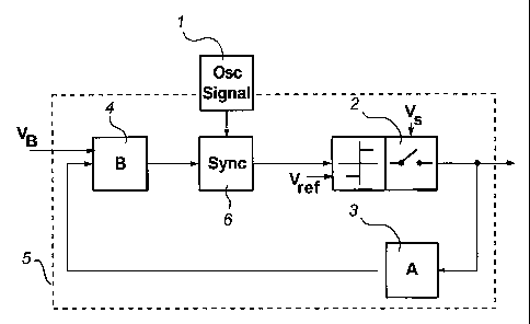
A power conversion system comprising a modulator
according to a first preferred embodiment of the
invention is shown in fig. 3. The system comprises a
power stage 2, a control system with a feedback block 3
and a forward block 4. The power stage 2 can comprise
one or a plurality of half-bridges, preferably a full-
bridge comprising two half-bridges. The feedback block
and the forward block constitute an oscillating modulator
5. An external signal source 1, also referred to as an
oscillating signal generator block, is connected to a
synchronization block 6 in the modulator 5.
The synchronization of the modulator 5 is obtained
by adding the Osc Signal from the source 1 to the
modulating signal. The synchronization signal can be
based on a voltage signal or a current signal depending
on the type of modulator (voltage based feedback or
current based feedback). The Osc Signal can be a
sinusoidal signal or any other oscillating signal with
CA 02470676 2004-06-15
WO 03/055060 PCT/IB02/05412
6
the frequency of the wanted idle switching frequency and
is used for synchronizing said modulator with said Osc
signal of the Osc Signal generating block 1.
A second preferred embodiment of the invention is
shown in fig. 4, where two COM modulators 10, 11 are
synchronized by one synchronizing signal from a
synchronization block 12. Again, the synchronization
signal can be based on a voltage signal or a current
signal depending on the type of modulator (voltage based
feedback or current based feedback).
The two COM modulators are designed to oscillate at
almost the same frequency, but a variation in the
switching frequency can be eliminated by the
synchronization means.
By the use of two COM modulators 10, 11 it is
possible to make a 3-level modulator. Each side of a load
13 is supplied with its own 2-level COM modulator 10, 11,
which each are synchronized.
The first harmonic of the carrier will ideally be
eliminated across the load. The input signal is inverted
by an inverter 14 preceding the second COM 11, in order
to be able to make a differential audio signal on the
output. The spectral characteristics resemble those of
the NBDD modulation. The NBDD can be seen from "Audio
power amplifier techniques with energy efficient power
conversion", Ph.D Thesis by Karsten Nielsen.
The use of said 3-level modulation can
advantageously be used for driving a pulse modulated
transducer directly without any output filtering of the
PWM signal thus reducing eddy current losses in the
transducer 6 compared to a 2-level modulation.
Fig 5 shows an example of a realization of the
synchronizing means in figs 3 and 4. The synchronization
means are implemented as a circuit of two series
resistances A, RB connected to each end of a parallel
circuit consisting of a resistor ROSC and a capacitor
COSC.
CA 02470676 2004-06-15
WO 03/055060 PCT/IB02/05412
7
By the use of this network a small amplitude signal
is added to the COM modulator forcing the COM modulator
to oscillate at the added small amplitude signal
frequency. Thereby one or a plurality of COM modulators
can be synchronized by adding a small amplitude signal
with the frequency of the. wanted idle frequency to each
of the modulators.
The values of the resistances and capacitors can be
determined by the skilled person in a trade-off between
having good synchronization and not having to influence
either of the modulators negatively.
A further preferred embodiment of the invention is
shown in Fig. 6 and illustrates an active synchronization
system for obtaining synchronization of COM modulators.
The active synchronization block 15 comprises one or a
plurality active high pass filters.
Fig. 7 gives an example of the active
synchronization block 15 in fig 6, implemented as two
active high pass filters 16, 17. One high pass filter 16
sums a first high pass filtered COM modulator signal at
node 18 to a second COM modulator signal at node 19 and
thereby synchronizes the second COM modulator with the
first. The optimal synchronization will be obtained if
also a second high pass filter 17 sums a high pass
filtered second modulator signal at node 19 to the first
modulator signal at node 18.
A power conversion system with two COM modulators,
synchronized according to the invention, is shown in Fig.
8. Two lag-blocks B1, B2 are inserted in the forward path
contributing to a higher loop gain at low frequencies.
There is not any high power filtering applied to the
system but the load, preferably an electro-dynamic
transducer, will act as an inductive load obtaining some
filtering of the PWM signal. Thereby the output filter
can be eliminated and efficiency increased. Each power
stage 20, 21 can comprise one or a plurality of half-
bridges, and preferably comprise a single half-bridge.
CA 02470676 2009-08-19
28371-97
8
The open loop gain for the system in Fig. 8 is shown
in Fig. 9. The system is designed for a switching
frequency of approximately 325kHz. At 325kHz the open
loop gain is 0 dB and at that frequency the phase is -180
degrees, obtaining a controlled oscillation. The system
shown in Fig-. 8 -will be capable- of. suppressing noise. and
distortion within the 325kHz bandwidth.
The system output is a differential 3-level PWM
signal with high frequency spectral characteristics
resembling those of the NBDD modulation obtaining a more
efficient modulation compared to modulation topologies
with a differential two level PWM-output signal.
If the modulators in the system shown in Fig. 9 are
completely synchronized, there will be a differential
output of zero magnitude at idle. This is caused by the
signal at idle on one terminal 22 of the load is equal to
the signal on the other terminal 23 of the load obtaining
a differential signal of zero magnitude.
The synchronization can be obtained by
synchronization means as shown in fig 5, as a
synchronization network comprising an R, C or RC circuit.
The R, C or RC circuit being connected to the comparator
in the forward path. The synchronization can also be
obtained as in fig 6 and 7, as an active network
comprising high pass active filter networks.
Furthermore the modulation depth can be controlled
by limiting the amplitude of the input signal at the
input signal node 24, achieving lower ripple currents.
Fig. 10 shows an SCOM according to the invention
implemented in multilevel PWM comprising a PSCPWM
modulator structure and a MECC(N,M) control system where
N,M are integers. MECC(N,M) is described in the
applicant's international patent application
PCT/DK97/00497. The system comprises one or a plurality
of feedback paths and low pass filtering of the output
PWM signal 25, 26.= With the SCOM system comprising a
PSCPWM modulator it is
CA 02470676 2004-06-15
WO 03/055060 PCT/IB02/05412
9
possible to obtain a multi-level (more than two levels)
modulator, preferably without high frequency common mode
components on the output. Each power stage 27, 28
comprises one or a plurality of half-bridges. If each
power stage 27, 28 comprises two half-bridges in a full-
bridge structure it is possible toobtain_a multi-level
(more than two levels) modulator, without high frequency
common mode components on the output.
In fig 11, N (where N is an integer) SCOM modulators
are synchronized by an additional synchronization signal.
This synchronization signal can be any signal shape but
preferably triangular, square or sinusoidal with a
frequency of the wanted idle switching frequency. The
synchronization means can be any one of those described
above.
In Fig. 12, N (where N is an integer) COM modulators
are synchronized by their common COM signals. The common
COM synchronization signal can be any signal shape with
the frequency of the wanted idle switching frequency. The
synchronization means can be any one of those described
above.
The SCOM modulator can be implemented in any given
AC-AC, DC-DC, AC-DC or DC-AC power conversion system, in
particular a high precision DC-AC audio power conversion
system where the power stage elements operates in either
"on" or "off" state.