Note: Descriptions are shown in the official language in which they were submitted.
CA 02470798 2004-06-11
MULTIPLE-ELEMENT ANTENNA WITH FLOATIN(a ANTENNA ELEMENT
FIELD OF THE INVENTION
This invention relates generally to the field of antennas. More specifically,
a
multiple-element antenna is provided that is particularly well-suited for use
in wireless
communication devices such as Personal Digital Assistants (PDAs), cellular
telephones,
and wireless two-way email communication devices.
BACKGROUND OF THE I1WENTION
Mobile communication devices ("mobile devices") having antenna structures that
support communications in multiple operating frequency bands are known. Many
different types of antennas for mobile devices are also known, including
helix, "inverted
F", folded dipole, and retractable antenna structures. Heliac and retractable
antennas are
typically installed outside a mobile device, and inverted F and folded dipole
antennas are
typically embedded inside a mobile device case or housing. Generally, embedded
antennas are preferred over external antennas for mobile devices for
mechanical and
ergonomic reasons. Embedded antennas are protected by the mobile device case
or
housing and therefore tend to be more durable than external antennas. Although
external
antennas may physically interfere with the surroundings of a mobile device and
make a
mobile device difficult to use, particularly in limited-space environments,
embedded
antennas present fewer such challenges. In some types of mobile device,
however, l~nown
embedded antenna structures and design techniques are not feasible where
operation in
multiple dissimilar frequency bands is required.
SUMMARY OF THE INVENTION
According to an aspect of the invention, a multiple-element antenna for a
wireless
communication device comprises a first antenna element having a first
operating
frequency band, a floating antenna element positioned adjacent the first
antenna element to
electromagnetically couple to the first antenna element and configured to
operate in
conjunction with the first antenna element within a second operating frequency
band, and
a feeding port connected to the first antenna element and configured to
connect the first
antenna element to communications circuitry and to exchange communication
signals in
1
CA 02470798 2004-06-11
both the first operating frequency band and the second operating frequency
band between
the multiple-element antenna and the communications circuitry.
A multiple-element antenna in accordance with another aspect of the invention,
for
use with a wireless mobile communication device having a transceiver and a
receiver,
comprises a single dielectric substrate, a first antenna element on the
dielectric substrate
having a feeding port connected to the transceiver and the receiver, and a
floating antenna
element on the dielectric substrate and positioned adjacent the first antenna
element on the
single dielectric substrate to electxomagnetically couple with the first
antenna element.
BRIEF DESCRIPTION OF THE DRAWINGS
Fig. I is a top view of a first antenna element;
Fig. 2 is a top view of a floating antenna element;
Fig. 3 is a top view of a multiple-element antenna including the antenna
elements
of Figs. 1 and 2;
Fig. 4 is an orthogonal view of the multiple-element antenna of Fig. 3 mounted
in a
mobile communication device;
Fig. 5 is a top view of a second antenna element;
Figs. 6-8 are top views of alternative second antenna elements;
Fig. 9 is a top view of a multiple-element antenna including a first antenna
element, a second antenna element, and a floating antenna element;
Fig. I O is a top view of a parasitic coupler;
Fig. 1 I is a top view of a:n alternative parasitic coupler;
Fig. 12 is a top view of a further multiple-element antenna including a
parasitic
coupler;
Fig. 13 is an orthogonal view of another multiple-element antenna mounted in a
mobile communication device; and
Fig. 14 is a block diagram of a mobile communication device.
DETAILED DESCRIPTION OF THE PREFERRED EMBODIMENTS
In a multiple-element antenna, different antenna elements are typically tuned
to
different operating frequency bands, thus enabling a multiple-element antenna
to function
as the antenna in a mufti-band mobile communication device. For example,
suitably tuned
separate antenna elements enable a multiple-element antenna for operation at
the Global
2
CA 02470798 2004-06-11
System for Mobile Communications (GSM) and General Packet Radio Service (GPRS)
frequency bands at approximately 900MHz and 1800MHz or 1900MHz, or at the Code
Division Multiple Access (CDMA) frequency bands at approximately 800MHz and
1900MHz.
Where operating frequency bands are relatively closely spaced, within 100-
200MHz, or sometimes where the bands are harmonically related, a single
antenna
element may be configured far mufti-band operation. In a GPRS mobile device,
for
example, operation in all three frequency bands may be desired to support
communications in networks in different countries or regions using a common
antenna
structure. In one known antenna design, tri-band operation is achieved using
only two
antenna structures connected to respective transceivers, including one antenna
element
tuned to 900MHz, and another antenna element tuned for operation within a
broader
frequency band including the two other frequency bands at 1800MHz and 1900MHz,
This
type of antenna structure enables three operating frequency bands using only
two antenna
elements.
However, as those skilled in the art of antenna design will appreciate, such
wide-
band operation of an antenna element sacrifices performance of the antenna
element in at
least one of the frequency bands covered by the broad operating frequency
band. Separate
antenna elements tuned to each of the two frequency bands generally exhibit
better
performance at each operating frequency band than a similar antenna element
configured
for wide-band operation. In addition, this wide-band technique is practical
only for
relatively closely spaced operating frequency bands, as described above.
Although a
single antenna element may be configured to operate at multiple similar or
closely spaced
frequency bands, operation in further "dissimilar" frequency bands is
typically supported
using a separate antenna element having its own feeding port for connection to
communications circuitry. As described in further detail below, multiple-
element
antennas according to aspects of the present invention include a first antenna
element
configured for operation in a first operating frequency band and a floating
antenna element
configured for operation in conjunction with the first antenna element at a
second
operating frequency band.
Fig. 1 is a top view of a first antenna element. The first antenna element 10
includes a first conductor section 22 and a second conductor section 26. The
first and
second conductor sections 22 and 26 are positioned to define a gap 23, thus
forming an
3
CA 02470798 2004-06-11
open-loop structure known as an open folded dipole antenna In alternative
embodiments,
other antenna designs may be utilized, such as a closed folded dipole
structure, for
example.
The first conductor section 22 includes a top load 20 that is used to set an
operating
frequency band of the first antenna element 10. As described briefly above,
this operating
frequency band may be a wide frequency band containing multiple operating
frequency
bands, such as 1804MHz and 1900MHz. The dimensions of the top load 20 affect
the
total electrical length of the first antenna element 10, and thus may be
adjusted to tune the
first antenna element 10. For example, decreasing the size of the top load 20
increases the
frequency of the operating frequency band of the first antenna element 10 by
decreasing
its total electrical length. In addition, the frequency of the operating
frequency band of the
first antenna element 10 may be further tuned by adjusting the size of the gap
23 between
the conductor sections 22 and 26, or by altering the dimensions of other
portions of the
f rst antenna element 10.
The second conductor section 26 includes a stability patch 24 and a load patch
28.
The stability patch 24 is a controlled coupling patch which affects the
electromagnetic
coupling between the first and second conductor sections 22 and 26 in the
operating
frequency band of the first antenna element 10. The electromagnetic coupling
between the
conductor sections 22 and 26 is further affected by the size of the gap 23,
which is selected
in accordance with desired antenna characteristics.
The first antenna element 10 also includes two ports I2 and 14, one connected
to
the first conductor section 22 and the other connected to the second conductor
section 26.
The ports 12 and I4 are offset from the gap 23 between the conductor sections
22 and 26,
resulting in a structure commonly referred to as an "offset feed" open folded
dipole
antenna. However, the ports 12 and 14 need not necessarily be offset from the
gap 23, and
may be positioned, for example, to provide space for, or so as not to
physically interfere
with, other components of a mobile device in which the first antenna element
10 is
implemented. The ports 12 and 14 are configured to couple the first antenna
element 10 to
communications circuitry. In one embodiment, the port I2 is coupled to a
ground plane,
while the port 14 is coupled to a signal source. The ground and signal source
connections
may be reversed in alternate embodiments, with the port 12 being coupled to a
signal
source and the port 14 being grounded. Although not shown in Fig. l, those
skilled in the
art will also appreciate that either or both of the ports 12 and 14 may be
connected to a
4
CA 02470798 2004-06-11
matching network, in order to match impedance of the first antenna element 10
with the
impedance of a communications circuit or device to which the antenna element
10 is
coupled.
Fig. 2 is a top view of a floating antenna element. The floating antenna
element 30
includes a patch 32, and conductor sections 34, 36, and 38. Those skilled in
the art will
appreciate that the dimensions of the patch 32 affect the operating frequency
band and
gain of an antenna incorporating the floating antenna element 30. As will be
described in
further detail below, the dimensions of the conductor sections 34, 36, and 38
control the
electromagnetic coupling between the floating antenna element 30 and another
antenna
IO element in conjunction with which it operates, and thus also affect the
operating
characteristics of an antenna including the floating antenna element 30.
Unlike the first
antenna element 10, the floating antenna element 30 does not include a feeding
port, and is
intended to operate in conjunction with another antenna element.
Fig. 3 is a top view of a multiple-element antenna including the antenna
elements
of Figs. 1 and 2. In the multiple-element antenna 40, the first antenna
element IO as
shown in Fig. 1 and the floating antenna element 30 of Fig. 2 are positioned
in close
proximity to each other, such that at least a portion of the first antenna
element 10 is
adjacent at least a portion of the floating antenna element 30. The multiple-
element
antenna 40 is fabricated on a flexible dielectric substrate 42, using copper
conductor and
known copper etching techniques, for example. The antenna elements 10 and 30
are
fabricated such that a portion of the first antenna element 10, the top load
20 of the first
conductor section 22 in Fig. 3, is adjacent to and partially overlaps the
conductor sections
34, 36, and 38 of the floating antenna element 30. The proximity of the first
antenna
element 10 and the floating antenna element 30 results in electromagnetic
coupling
between the two antenna elements 10 and 30.
The first antenna element 10 is either tuned to optimize a single frequency
band,
such as the CDMA Personal Communication System (PCS) 1900MHz band, or
configured
for wide-band operation in multiple frequency bands, such as GSM-1800
(1800MHz), also
known as DCS, and GSM-1900 (1900MHz) in a GPRS device, for example. The
floating
antenna element 30 is tuned to optimize a dissimilar operating frequency band
of the
multiple-element antenna 40. The dissimilar operating frequency band is
determined by
the overall length of the first antenna element 10 and the floating antenna
element 30. In
one embodiment of the invention, the floating antenna 30 enables the multiple-
element
5
CA 02470798 2004-06-11
antenna 40 to receive Global Positioning System (GPS) signals in a frequency
band of
1575MHz, although it should be appreciated that the invention is in no way
restricted
thereto. The principles described herein may also be applied to other
frequency bands.
As described above, the operating characteristics of the first antenna element
10
are controlled by adjusting the dimensions of the conductor sections 22 and 26
and the size
of the gap 23 between the first and second conductor sections 22 and 26. For
example, the
gap 23 is adjusted to tune the first antenna element IO to a selected first
operating
frequency band by optimizing antenna gain and performance at a particular
frequency
within the first operating frequency band. The dimensions of the stability
patch 24 and the
gap 23 affect the input impedance of the first antenna element 10, and as such
are also
adjusted to improve impedance matching between the first antenna element 10
and
communications circuitry to which it is connected. In a similar manner, the
dimensions of
the patch 32 affect the operating frequency band, gain, and impedance of the
multiple-
element antenna 40.
The dimensions of each of the antenna elements 10 and 30 and the spacing
therebetween also control the electromagnetic coupling between the antenna
elements.
Proper control of the electromagnetic coupling between the antenna elements 10
and 30
provides for substantially independent tuning of each operating frequency
band.. The
dimensions of each antenna element 10 and 30 and its position relative to the
other
antenna element are therefore adjusted so that the antenna element I0 and the
antenna 40
are optimized within their respective operating frequency bands. In the
multiple-element
antenna 40, the conductor sections 34 and 38, and to a lesser degree, the
conductor section
36, overlap portions of the top load 20 of the first antenna element 10. These
portions of
the antenna elements 10 and 30 primarily control the strength of the
electromagnetic
coupling between the antenna elements 10 and 30, as well as the impedance,
particularly
capacitance, of the multiple-element antenna 40.
In operation, the first antenna element 10 of the multiple-element antenna 40
enables communications in a first operating frequency band, and the
combination of the
first antenna element IO and the floating antenna element 30 enable
communications in a
second operating frequency band.
The first antenna element 10 is operable to transmit and/or receive
commuzucation
signals in the first operating frequency band. Although the floating antenna
element 30
presents a top load to the first antenna element 10 due to the electromagnetic
coupling
6
CA 02470798 2004-06-11
described above, proper adjustment of the dimensions and placement of the
antenna
elements compensates for or reduces the effects of the floating antenna
element 30 on the
operation of the first antenna element 10 in the first operating frequency
band. Thus, the
first antenna element 10 forms the primary radiator for transmission and
reception of
communication signals in the first operating frequency band. Communication
signals
received by the first antenna element 10 are transferred to communications
circuitry (not
shown) to which the ports 12 and 14 are connected. Similarly, communications
signals
that are to be transmitted in the first operating frequency band are
transferred to the first
antenna element 10 through the ports 12 and 14. Transmission and reception
functions in
the first frequency band are dependent upon the type of communications
circuitry to which
the ports 12 and 14 are connected. For example, the communications circuitry
may
include a receiver, a transmitter, or a transceiver incorporating both a
receiver and a
transmitter.
Operation of the multiple-element antenna 40 in the second operating frequency
band exploits the electromagnetic coupling between the floating antenna
element 30 and
the first antenna element 10. The first antenna elemenl; 10 and the floating
antenna
element 30 operate in combination to receive, and to transmit in some
embodiments of the
invention, communication signals in the second operating frequency band. These
signals
are transferred between the multiple-element antenna 40 and associated
communications
circuitry through the ports 12 and 14. The ports 12 and 14 of the first
antenna element 10
thus act as a feeding port for both the first antenna element 10 and, through
the
electromagnetic coupling between the antenna elements 10 and 30, the multiple-
element
antenna 40.
As will be apparent from the foregoing description, the design of a multiple-
element antenna such a.s 40 involves a trade off between loading the first
antenna element
10 in the first operating frequency band and ensuring effective operation of
the multiple-
element antenna 40 in the second operating frequency band. Whereas the
electromagnetic
coupling between the antenna elements 10 and 30 introduces a top load to the
first antenna
element 10, this same coupling principle enables operation of the multiple-
element
antenna 40 in the second operating frequency band from the ports 12 and 14 of
the first
antenna element 10.
The communications circuitry associated with the first and second operating
frequency bands is either a single receiver, transmitter, or transceiver
configured to
7
CA 02470798 2004-06-11
operate in multiple frequency bands, or distinct receivers, transmitters,
transceivers, or
some combination thereof for each frequency band. In one: possible
implementation, for
example, the first operating frequency band is the 1900MHz GDMA PCS frequency
band,
the second operating frequency band is the 1575MHz GP S frequency band, and
both a
CDMA transceiver and a GPS receiver are connected to the ports 12 and 14.
Fig. 3 represents a multiple-element antenna according to one embodiment of
the
present invention. In alternative embodiments, the antenna elements 10 and 30
or parts
thereof may overlap to a greater or lesser degree. For example, increasing the
spacing
between the top load 20 and the conductor section 38, or decreasing the
lengths of the
conductor section 34, 36, or 38 to thereby decrease the degree of overlap
between the
antenna elements 10 and 30 reduces the electromagnetic coupling between the
antenna
elements 10 and 30 and also affects the impedance of the multiple-element
antenna 40.
Those skilled in the art will also appreciate that electromagnetic coupling
may be achieved
without necessarily overlapping portions of the antenna elements 10 and 30.
Therefore,
other structures than the particular structure shown in Fig. 3 are also
possible. The
dimensions and spacing of antenna elements in such alternate structures, and
thus the
electromagnetic coupling between the antenna elements, are preferably adjusted
so that
optimum antenna efficiency and substantially independent antenna element
tuning are
achieved, as described above.
Fig. 4 is an orthogonal view of the multiple-element antenna of Fig. 3 mounted
in a
mobile communication device. Those skilled in the art will appreciate that a
front housing
wall and a majority of internal components of the mobile device 43, which
would obscure
the view of the antenna, have not been shown in Fig. 4. In an assembled mobile
device,
the embedded antenna shown in Fig. 4 is not visible.
The mobile device 43 comprises a case or housing having a front wall (not
shown),
a rear wall 44, a top wall 46, a bottom wall 47, and side walls, one of which
is shown at
45. In addition, the mobile device 43 includes a transceiver 48 and a receiver
49
connected to the ports 12 and 14 of the first antenna element 10 and mounted
within the
housing.
Although the portion of the substrate 42 behind the top wall 46 has not been
shown
in Fig. 4 in order to avoid congestion in that portion of the drawing, it
should be
understood that the substrate extends along the side wall 45 and onto the top
wall 46 at
least as far as the end of the floating antenna element 30. Fabrication of the
multiple-
8
CA 02470798 2004-06-11
element antenna 40 on the substrate 42, preferably a flexible dielectric
substrate, facilitates
handling of the antenna before and during installation in the mobile device
43.
The multiple-element antenna, including the substrate 42 on which the antenna
is
fabricated, is mounted on the inside of the housing of the mobile device 43.
The substrate
42 and thus the multiple-element antenna is folded from an original,
substantially flat
configuration such as illustrated in Fig. 3, so as to extend around the inside
surface of the
mobile device housing to orient the antenna in multiple planes. The first
antenna element
is folded and mounted along the rear, side, and top walls 44, 45, and 46. The
ports 12
and 14 are mounted on the rear wall 44 and connected to both the transceiver
48 a~ld the
10 receiver 49. The first conductor section 22 extends along the side wall 45,
around the top
corner 39, and along and the top wall 46. The floating antenna element 30
similarly
extends along the side wall 45, the top wall 46, and the rear wall 44. As
shown, the
floating antenna element is positioned partially on the top wall 46, with the
conductor
section 38 extending onto the side wall 45 and a portion 35 of the patch 32
extending
around the top rear edge 41 onto the rear wall 44.
The ports 12 and 14 of the first antenna element 10 are connected to both the
transceiver 48 and the receiver 49. Switching or routing of signals to and
from one or the
other of the transceiver 48 and the receiver 49 may be accomplished in many
ways, as will
be apparent to those skilled in the art. As described briefly above, the first
antenna
element 10 is configured for operation within the 1900MHz CDMA PCS frequency
band,
the floating antenna element 30 operates in combination with the first antenna
element 10
at the 1575MHz GPS frequency band, the transceiver 48 is a CDMA PCS
transceiver, and
the receiver 49 is a GPS receiver in one possible implementation. Mounting of
the
floating antenna element 30 on the top wall 46 of the mobile device 43 is
particularly
advantageous for effective reception of signals from GPS satellites, since a
mobile device
is typically oriented with its top surface relatively unobstructed and facing
toward the sky,
when the mobile device is in use or stored in a storage cradle or carrying
case, for
example. In addition, other components of the mobile device 43 block radiation
components associated with the floating antenna element; 30 that are directed
into the
device. This blocking has a resultant beam-shaping effect that enhances
components
directed out of the top of the device and further improves GPS signal
reception.
As shown, the patch 32 comprises a portion 35 which extends around the top
rear
edge 41 and onto the rear wall 44. This portion 35 is used, for example, where
9
CA 02470798 2004-06-11
electromagnetic coupling between the floating antenna element 30 and other
components
of the mobile device 43 is desired. Such coupling to other device components
provides a
further degree of freedom for controlling the radiation pattern of the
multiple-element
antenna. Thus, in alternate embodiments, the patch 32 is mounted entirely or
only
partially on the top wall 46.
Although Fig. 4 shows one orientation of the multiple-element antenna within
the
mobile device 43, it should be appreciated that the antenna may be mounted in
different
ways, depending upon the type of housing, for example. In a mobile device with
substantially continuous rear, top, side, and bottom walls, an antenna may be
mounted
directly to the housing. Many mobile device housings are fabricated in
separate parts that
are attached together when internal components of the mobile device have been
placed.
Often, the housing sections include a front section and a rear section, each
including a
portion of the top, side and bottom walls of the housing. Unless the portion
of the top,
side, and bottom walls in the rear housing section is of sufficient size to
accommodate the
antenna and the substrate, then mounting of the antenna on the housing as
shown in Fig. 4
might not be practical. In such mobile devices, the antenna is preferably
attached to an
antenna frame that is integral with or adapted to be mounted on the mobile
device housing,
a structural member in the mobile device, or another component of the mobile
device.
Where the antenna is fabricated on a substrate, mounting ar attachment of the
antenna is
preferably accomplished using an adhesive provided on or applied to the
substrate, the
component to which the antenna is mounted or attached, or both.
The mounting of the multiple-element antenna as shown in Fig. 4 is intended
for
illustrative purposes only. T'he multiple-element antenna or other similar
antenna
structures may be mounted on different surfaces of a mobile device or mobile
device
housing. For example, housing surfaces on which a multiple-element antenna is
mounted
need not necessarily be flat, perpendicular, or any particular shape. An
antenna may also
be mounted on fewer or further surfaces or planes than shown in Fig. 4.
Although the preceding description relates to a two-element antenna, it should
be
appreciated that a floating antenna element may be implemented in multiple-
element
antennas having more than one other antenna element. Illustrative examples of
multiple
element antennas incorporating a first antenna element, a second antenna
element, and a
floating antenna element are described below.
CA 02470798 2004-06-11
Fig. 5 is a top view of a second antenna element. The second antenna element
50
includes a first port 52, a second port 54, and a top conductor section 56
connected to the
ports 52 and 54. As will be apparent to those skilled in the art, the ports 52
and 54 and the
top conductor section 56 are normally fabricated from conductive material such
as copper,
for example. The length of the top conductor section 56 sets an operating
frequency band
of the second antenna element 50.
Figs. 6-8 are top views of alternative second antenna elements. Whereas the
top
conductor section 56 of the second antenna element 50 has substantially
uniform width 58,
the alternative second antenna element 60 shown in Fig. 6 has a top conductor
section 66
with non-uniform width. As shown in Fig. 6, the portion 68 between the ports
62 and 64
and part of the top conductor section 66 of the antenna element 60 have a
width 67, and an
end portion of the antenna element 60 has a smaller width 69. A structure as
shown in
Fig. 6 is useful, for example, to provide space for other antenna elements,
such as a
parasitic coupler, in order to conserve space. As those skilled in the art
will appreciate, the
length and width of the antenna element 60 or portions thereof are selected to
set gain,
bandwidth, impedance match, operating frequency band, and other
characteristics of the
antenna element.
Fig. 7 shows a top view of a further alternative second antenna element. The
antenna element 70 includes ports 72 and 74, and first, second and third
conductor
sections 75, 76 and 78. The operating frequency band of the antenna element 70
is
primarily controlled by selecting the lengths of the second and third
conductor sections 76
and 78. Any of the lengths L3, L4 and L5 may be adjusted to set the lengths of
the second
and third conductor sections 76 and 78, whereas the length of the first
conductor section
75 may be set for impedance matching purposes by adjusting the lengths L1, L2,
or both.
Although the lengths of the i:irst, second and third conductor sections are
adjusted to
control the above operating characteristics of the antenna element 70,
adjustment of the
length of any of these eanductor sections has some effect on the
characteristic controlled
primarily by the other antenna conductor sections. For example, increasing L3,
I,4 or L5
to decrease the operating frequency band of the antenna element 70 may also
necessitate
adjustment of one or both of the lengths Ll and L2, since changing L3, L4 or
L5 also
affects the impedance and thus the matching of the antenna element 70.
Any of the first, second and third conductor sections of the antenna element
70
may include a structure to increase its electrical length, such a.s a
meandering line or
11
CA 02470798 2004-06-11
sawtooth pattern, for example. Fig. 8 is a top view of another alternative
first antenna
element, similar to the antenna element 70, including ports 82 and 84 and
.meandering
lines 90, 92 and 94 to increase the electrical length of the first, second and
third conductor
sections 85, 86 and 88. The meandering lines 92 and 94 change the lengths of
the second
and third conductor sections 86 and 88 of the second antenna element 80 in
order to tune it
to a particular operating frequency band. The meandering line 94 also top-
loads the
second antenna element 80 such that it operates as though its electrical
length were greater
than its actual physical dimension. The meandering line 90 similarly changes
the
electrical length of the first conductor section for impedance matching. The
electrical
length of the any of the meandering lines 90, 92 and 94, and thus the total
electrical length
of the first, second and third conductor sections 85, 86 and 88, may be
adjusted, for
example, by connecting together one or more segments of the meandering lines
to form a
solid conductor section.
Fig. 9 is a top view of a multiple-element antenna including a first antenna
element, a second antenna element, and a floating antenna element. In the
multiple
element antenna 100, a first antenna element 10 and a floating antenna element
30 are
positioned adjacent each other on a substrate 102. The floating antenna 30
operates in
conjunction with the first antenna element 10 substantially as described
above.
The second antenna element 50 as shown in Fig. 5 is positioned such that at
least a
portion of the second antenna element 50 is adjacent at least a portion of the
first antenna
element 10. In Fig. 9, the antenna elements 10 and 50 are fabricated on the
substrate 102
such that a portion of the top conductor section 56 of the second antenna
element 50 is
adjacent to and partially overlaps the second conductor section 26 of the
first second
antenna element 10. The proximity of the first antenna element 10 and the
second antenna
element 50 results in electromagnetic coupling between the two antenna
elements 10 and
50. Although the first antenna element 10 and the second antenna element 50
are typically
tuned to optimize corresponding first and second operating frequency bands,
each antenna
element 10 and 50 acts as a parasitic element to the other due to the
electromagnetic
coupling therebetween, thus improving performance of the multiple-element
antenna 100
by smoothing current distributions in each antenna element IO and 50 and
increasing the
gain and bandwidth at the operating frequency bands of both the first and
second antenna
elements 10 and 50. For example, in a mobile device designed for operation in
a GPRS
network, the first operating frequency band may include both the GSM-1800
(1800MHz)
12
CA 02470798 2004-06-11
or DCS, and the GSM-1900 (1900MHz) or PCS frequency bands, whereas the second
operating frequency band is the GSM-900 (900MHz) frequency band. In a CDMA
mobile
device, the first and second operating frequency bands may include the CDMA
bands at
approximately 1900MHz and 800MHz, respectively. Those skilled in the art will
appreciate that the first and second antenna elements 10 and 50 may be tuned
to other first
and second operating frequency bands for operation in different communication
networks.
Fig. 9 represents an illustrative example of a multiple-element antenna. The
dimensions, shapes, and orientations of the various patches, gaps, and
conductors that
affect the electromagnetic coupling between the elements 10, 30, and 50 may be
modified
to achieve desired antenna characteristics. For example, although the second
antenna
element 50 is shown in the multiple-element antenna 100, any of the
alternative antenna
elements 60, 70, and 80, or a second antenna element combining some of the
features of
these alternative second antenna elements, could be used instead of the second
antenna
element 50. Other forms of the first antenna element 10 and the floating
antenna element
30 may also be used in alternative embodiments.
Fig. 10 is a top view of a parasitic coupler. A parasitic coupler is a
parasitic
element, a single conductor 110 in Fig. 10, which is used to improve
electromagnetic
coupling between first and second antenna elements, as described in further
detail below,
to thereby improve the performance of each antenna element in its respective
operating
frequency band and smooth current distributions in the antenna elements.
A parasitic coupler need not necessarily be a substantially straight conductor
as
shown in Fig. 10. Fig. 11 is a top view of an alternative parasitic coupler.
The parasitic
coupler 112 is a folded or curved conductor which has a first conductor
section 114 and a
second conductor section 116. A parasitic coupler such as 112 is used, for
example, where
physical space limitations exist.
It should also be appreciated that a parasitic coupler may alternatively
comprise
adjacent, connected or disconnected, conductor sections. For example, two
conductor
sections of the type shown in Fig. 10 could be juxtaposed so that they overlap
along
substantially their entire lengths to form a "stacked" parasitic element. In a
variation of a
stacked parasitic element, the conductor sections only partially overlap, to
form an offset
stacked parasitic element. End-to-end stacked conductor sections represent a
further
variation of multiple-conductor section parasitic elements. Other parasitic
element
patterns or structures, adapted to be accommodated within available physical
space or to
13
CA 02470798 2004-06-11
achieve particular electromagnetic coupling and performance characteristics,
will also be
apparent to those skilled in the art.
Fig. 12 is a top view of a further multiple-element antenna including a
parasitic
coupler. The multiple-element antenna 111 includes the first and second
antenna elements
10 and 50, the floating antenna element 30, and the parasitic coupler 112. As
shown, the
parasitic coupler 112 is adjacent to and overlaps a portion of both the first
antenna element
and the second antenna element 50.
In the multiple-element antenna 111, part of the first conductor section 114
of the
parasitic coupler 112 is positioned adjacent to the top conductor section 56
of the second
10 antenna element 50 and electrornagnetically couples therewith. The second
conductor
section 116 and a portion of the first conductor section 114 of the parasitic
coupler 12
similarly overlap a portion of the first antenna element 10 in order to
electromagnetically
couple the parasitic coupler 112 with the first antenna element 10. The
parasitic coupler
112 thereby electromagnetically couples with both the first antenna element 10
and the
second antenna element 50.
The second antenna element 50 tends to exhibit relatively poor communication
signal radiation and reception in some types of mobile devices. Particularly
when
implemented in a small mobile device, the length of the top conductor section
56 is limited
by the physical dimensions of the mobile device, resulting in poor gain. The
presence of
the parasitic coupler 112 enhances electromagnetic coupling between the first
antenna
element 10 and the second antenna element 50. Since the first antenna element
10
generally has better gain than the second antenna element 50, this enhanced
electromagnetic coupling to the first antenna element 10 improves the gain of
the second
antenna element 50 in its operating frequency band. When operating in its
operating
frequency band, the second antenna element 50, by virtue of its position
relative to the first
antenna element 10, electromagnetically couples to the second conductor
section 26 of the
first antenna element 10. Through the parasitic coupler 112, the second
antenna element
50 is more strongly coupled to the second conductor section 26 and also
electromagnetically couples to the first conductor section 22 of the first
antenna element
10.
The parasitic coupler 112 also improves performance of the first antenna
element
10, and thus, the performance of the multiple-element antenna 40 in all of its
operating
frequency bands. In particular, the parasitic coupler 112, through its
electromagnetic
14
CA 02470798 2004-06-11
coupling with the first antenna element 10, provides a further conductor to
which current
in the first antenna element 10 is effectively transferred, resulting in a
more even current
distribution in the first antenna element 10. Electromagnetic coupling from
both the first
antenna element 10 and the parasitic coupler 112 to the second antenna element
50 also
disperses current in the first antenna element 10 and the parasitic coupler
112. This
provides for an even greater capacity for smoothing current distribution in
the first antenna
element 10, in that current can effectively be transferred to both the
parasitic coupler 112
and the second antenna element 50 when the first antenna element 10 is in
operation, when
a communication signal is being transmitted or received in an operating
frequency band
associated with either the first antenna element 10 or the multiple-element
antenna 40, for
example.
The length of the parasitic coupler 112, as well as the spacing between the
first and
second antenna elements 10 and 50 and the parasitic coupler 112, control the
electromagnetic coupling between the antenna elements 10 and 50 and the
parasitic
coupler 112, and thus are adjusted to control the gain and bandwidth of the
first antenna
element 10 and the second antenna element 50 within their respective first
arid second
operating frequency bands.
Operation of the antenna 111 is otherwise substantially as described above in
conjunction with Fig. 9.
Although particular types of antenna elements and parasitic elements are shown
in
Fig. 12, the present invention is in no way restricted thereto. Alternative
embodiments in
which other types of elements are implemented are also contemplated,
including, for
example, antenna elements incorporating features of one or more of the
alternative antenna
elements in Figs. 6-8. The relative positions of the various elements in the
antenna 111
may also be different than shown in Fig. 12 for alternative embodiments.
Electromagnetic
coupling between the first and second antenna elements 10 and 50 is enhanced,
for
example, by locating the parasitic coupler 112 between the first and second
antenna
elements 10 and 50. Such an alternative structure provides tighter coupling
between the
antenna elements. However, an antenna such as the antenna 111, with a weaker
coupling
between the antenna elements, is useful when some degree of isolation between
the first
and second antenna elements 10 and 50 is desired.
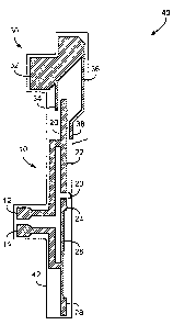
Fig. 13 is an orthogonal view of another multiple-element antenna mounted in a
mobile comrnunieation device. As in Fig. 4, a front housing wall and a
majority of
CA 02470798 2004-06-11
internal components of the mobile device 120, which would obscure the view of
the
antenna, have not been shown in Fig. 13.
The mobile device 120 comprises a case or housing having a front wall (not
shown), a rear wall 123, a top wall 128, a bottom wall 126, and side walls,
one of which is
shown at 124. In addition, the mobile device 120 includes a first transceiver
136, a second
transceiver 134, and a receiver 138 mounted within the housing.
The multiple-element antenna shown in Fig. 13 is similar to the multiple-
element
antenna 111 in Fig. 12 in that it includes a first antenna element 150, a
second antenna
element 140, a floating antenna element 160, and a parasitic coupler 170. The
first
antenna element 150 is a dipole antenna element, having a port 152 connected
to a first
conductor section 158 and a second port 154 connected to a second conductor
section 156.
The ports 152 and 154 are also configured for connection to both the first
transceiver 136
and the receiver 138, through one of many possible signal switching or routing
arrangements (not shown). The second antenna element 140 is similar to the
antenna
element 50, and comprises ports 142 and 144, configured to be connected to the
second
transceiver 144, and a top conductor section 1.46. The antenna elements 140,
150, and 160
and the parasitic coupler 170 are fabricated on a substrate 172. As in Fig. 4,
the portion of
the substrate 172 behind the top wall 128 has not been shown in Fig. 13.
Fig. 13 shows further examples of the possible shapes and types of elements to
which the present invention is applicable. The first antenna element 150 is a
different
dipole antenna element than the antenna element 10. For example, the first
conductor
section 158 includes an extension 166 which improves coupling between the
first antenna
element 10 and the floating antenna element 160, the port 154 is connected to
one end of
the second conductor section 156 instead of to an intermediate portion
thereof, and both
conductor sections are shaped differently than those in the antenna element
10. The
second antenna element 140 is also different than the second antenna element
50 in the
multiple-element antennas of Figs. 9 and 12, in that the top conductor section
146 has non-
uniform width, and includes a notch or cut-away portion in which the parasitic
coupler 170
is nested. Further shape, size, and relative position variations will be
apparent to those
skilled in the art and as such are considered to be within the scope of the
present invention.
The multiple-element antenna, including the substrate 172 on which the antenna
is
fabricated, is mounted inside the housing of the mobile device 120, directly
on the
housing, on a mounting frame attached to the housing or another structural
part of the
16
CA 02470798 2004-06-11
mobile device 120, or on some other part of the mobile device 120. The
substrate 172 and
thus the multiple-element antenna are folded from an original, substantially
flat
configuration such as illustrated in Fig. 12 to orient the antenna in multiple
planes.
The first antenna element 150 is folded and mounted across the rear, side, and
top
walls 123, 124, and 128. The ports 152 and 154 are mounted on the rear wall
123 and
connected to the first transceiver 136 and the receiver 138. The first
conductor section
158 extends along the side wall 124, around the top corner 132, and along and
the top wall
128. The second conductor section 156 of the first antenna element 150 is
mounted on the
side wall 124.
The top conductor section 146 of the second antenna element 140 is mounted on
the side wall 124 and extends from the side wall 124 around a bottom corner
130 to the
bottom wall 126. The ports 142 and 144 are mounted on the rear wall 123 of the
housing
and connected to the second transceiver 134. As shown, the parasitic coupler
170 is
mounted to the side wall 124.
The floating antenna element 160 is mounted partially along the top housing
wall
128, with a conductor section 164 on the top wall 128 and a conductor section
168
extending along the top wall 128, around the corner 132 anal onto the side
wall 124. The
floating antenna element 160 also includes a patch, of which a portion 162
extends around
a top rear edge of the housing and onto the rear wall 123. As described above,
this
location of the floating antenna 160 is particularly advantageous where the
receiver 138 is
a GPS receiver.
A mobile device in which a multiple-element antenna is implemented may, for
example, be a data communication device, a voice communication device, a dual-
mode
communication device such as a mobile telephone having data communications
functionality, a personal digital assistant (PDA) enabled for wireless
communications, a
wireless email communication device, or a wireless modem operating in
conjunction with
a laptop or desktop computer or some other electronic device or system.
Fig. 14 is a block diagram of a mobile communication device. The mobile device
120 is a dual-mode mobile device and includes a transceiver module 911, a
microprocessor 938, a display 922, a non-volatile memory 924, random access
memory
(RAM) 926, one or more auxiliary inputloutput (I/O) devices 928, a serial port
930, a
keyboard 932, a speaker 934, a microphone 936, a short-range wireless
communications
sub-system 940, and other device sub-systems 942.
17
CA 02470798 2004-06-11
The transceiver module 911 includes first and second antennas 902 and 904, a
first
transceiver 906, a receiver 908, a second transceiver 910, and a digital
signal processor
(DSP) 920. Although not shown separately in Fig. 14, it will be apparent from
the
foregoing description that the first antenna 906 includes both a first antenna
element and a
floating antenna element. In a preferred embodiment, the first and second
antennas 902
and 904 are antenna elements in a multiple-element antenna.
Within the non-volatile memory 924, the mobile device 120 preferably includes
a
plurality of software modules 924A-924N that can be executed by the
microprocessor 938
(and/or the DSP 920), including a voice communication module 924A, a data
communication module 924B, and a plurality of other operational modules 924N
for
carrying out a plurality of other functions.
The mobile device 120 is preferably a two-way communication device having
voice and data communication capabilities. Thus, for example, the mobile
device 120
may communicate over a voice network, such as any of the analog or digital
cellular
networks, and may also communicate over a data network. The voice and data
networks
are depicted in Fig. I4 by the communication tower 919. These voice and data
networks
may be separate communication networks using separate infrastructure, such as
base
stations, network controllers, etc., or they may be integrated into a single
wireless
network. The transceivers 906 and 910 and the receiver 908 are normally
configured to
communicate with different networks 919.
The transceiver module 911 is used to communicate with the networks 919. The
DSP 920 is used to send and receive communication signals to and from the
transceivers
906 and 910 and to receive communications signals from the receiver 908, and
provides
control information to the transceivers 906 and 910 and the receiver 908.
Information,
which includes both voice and data information, is communicated to and from
the
transceiver module 911 via a link between the DSP 920 and the microprocessor
938.
The detailed design of the transceiver module 911, such as operating frequency
bands, component selection, power level, etc., is dependent upon the
communication
network 919 in which the mobile device I20 is intended to operate. For
example, in a
mobile device intended to operate in a North American market, the first
transceiver 906
may be designed to operate with any of a variety of voice communication
networks, such
as the Mobitex~ or DataTACTM mobile data communication networks, AMPS, TDMA,
CDMA, PCS, etc., whereas the receiver 908 is a GPS receiver configured to
operate with
18
CA 02470798 2004-06-11
GPS satellites and the second transceiver 910 is configured to operate with
the GPRS data
communication network and the GSM voice communication network in North America
and possibly other geographical regions. Other types of data and voice
networks, both
separate and integrated, may also be utilized with a mobile device 120. The
transceivers
906 and 910 rnay instead be configured for operation in different operating
frequency
bands of similar networks, such as GSM-900 and GSM-1900, or the CDMA bands of
800MHz and 1900MHz, for example. In some instances, a third transceiver is
implemented instead of the receiver 908.
Depending upon the type of network or networks 919, the access requirements
for
the mobile device 120 may also vary. For example, in the Mobitex and DataTAC
data
networks, mobile devices are registered on the network using a unique
identification
number associated with each mobile device. In GPRS data networks, however,
network
access is associated with a subscriber or user of a mobile device. A GPRS
device typically
requires a subscriber identity module ("SIM") in order to operate a mobile
device on a
GPRS network. Local or non-network communication functions (if any) may be
operable,
without the SIM device, but a mobile device will be unable to carry out any
functions
involving communications over the data network 919, other than any legally
required
operations, such as '911' emergency calling.
After any required network registration or activation procedures have been
completed, the mobile device 120 may the send and receive communication
signals,
including both voice and data signals, over the networks 919. Signals received
by the
antenna 902 or 904 from the communication network 919 are routed to one of the
transceivers 906 and 910 or the receiver 908, which provide for signal
amplification,
frequency down conversion, filtering, and channel selection, for example, as
well as
analog to digital conversion. Analog to digital conversion of the received
signal allows
more complex communication functions, such as digital demodulation and
decoding to be
performed using the DSP 920. In a similar manner, sig~lals to be transmitted
to the
network 919 are processed, including modulation and encoding, for example, by
the DSP
920 and are then provided to one of the transceivers 906 and 910 fox digital
to analog
conversion, frequency up conversion, filtering, amplification and transmission
to the
communication network 919 via the antenna 902 or 904.
In addition to processing the communication signals, the DSP 920 also provides
for
transceiver control. For example, the gain levels applied to communication
signals in the
19
CA 02470798 2004-06-11
transceivers 906 and 910 or the receiver 908 may be adaptively controlled
through
automatic gain control algorithms implemented in the DSP 920. Other
transceiver control
algorithms could also be implemented in the DSP 920 in order to provide more
sophisticated control of the transceiver module 911.
S The microprocessor 938 preferably manages and controls the overall operation
of
the dual-mode mobile device 120. Many types of microprocessors or
microcontrollers
could be used here, or, alternatively, a single DSP 920 could be used to carry
out the
functions of the microprocessor 938. Low-level communication functions,
including at
least data and voice communications, are performed through the DSP 920 in the
transceiver module 911. Other, high-level communication applications, such as
a voice
communication application 924A, and a data communication application 9248 may
be
stored in the non-volatile memory 924 for execution by the microprocessor 938.
For
example, the voice communication module 924A provides a high-level user
interface
operable to transmit and receive voice calls between the mobile device 120 and
a plurality
of other voice or dual-mode devices via the networks 919. Similarly, the data
communication module 9248 provides a high-level user interface operable for
sending and
receiving data, such as e-mail messages, files, organizer information, short
text messages,
etc., between the mobile device 120 and a plurality of other data devices via
the networks
919. The microprocessor 938 also interacts with other device subsystems, such
as the
display 922, the non-volatile memory 924, the RAM 926, the auxiliary
input/output (I/O)
subsystems 928, the serial port 930, the keyboard 932, the speaker 934, the
microphone
936, the short-range communications subsystem 940 and any other device
subsystems
generally designated as 942.
Some of the subsystems shown in Fig. 14 perform communication-related
functions, whereas other subsystems may provide "resident" or on-device
functions.
Notably, some subsystems, such as the keyboard 932 and the display 922 are
used for both
communication-related functions, such as entering a text message for
transmission over a
data communication network, and device-resident functions such as a
calculator, task list,
or other PDA type functions.
Operating system software used by the microprocessor 938 is preferably stored
in a
persistent store such as the non-volatile memory 924. In addition to the
operation system,
which controls all of the low-level functions of the mobile device 120, the
non-volatile
memory 924 may include a plurality of high-level software application
programs, or
CA 02470798 2004-06-11
modules, such as the voice communication module 924A, the data communication
module
924B, an organizer module (not shown), or any other type of software module
924N.
These soi~ware modules are executed by the microprocessor 938 and provide a
high-level
interface between a user and the mobile device 120. This interface typically
includes a
S graphical component provided through the display 922, and an input/output
component
provided through the auxiliary I/O 928, the keyboard 932, the speaker 934, and
the
microphone 936. The operating system, specific device applications or modules,
or parts
thereof, may be temporarily loaded into a volatile store such as the RAM 926
for faster
operation. Moreover, received communication signals may also be temporarily
stored to
the RAM 926, before permanently writing them to a file system located in a
persistent
store such as the non-volatile memory 924. The non-volatile memory 924 may be
implemented, for example, as a Flash memory component, or a battery backed-up
RAM.
An exemplary application module 924N that may be loaded onto the mobile device
120 is a personal information manager (PIM) application providing PDA
functionality,
such as calendar events, appointments, and task items. This module 924N may
also
interact with the voice communication module 924A for managing phone calls,
voice
mails, etc., and may also interact with the data communication module for
managing e
mail communications and other data transmissions. Alternatively, all of the
functionality
of the voice communication module 924A and the data communication module 924B
may
be integrated into the PIM module.
The non-volatile memory 924 preferably provides a file system to facilitate
storage
of PIM data items and other data on the mobile device 120. The PIM application
preferably includes the ability to send and receive data items, either by
itself, or in
conjunction with the voice and data communication modules 924A and 9248, via
the
wireless networks 919. The PIM data items are preferably seamlessly
integrated,
synchronized and updated, via the wireless networks 919, with a corresponding
set of data
items stored or associated with a host computer system, thereby creating a
mirrored
system for data items associated with a particular user.
The mobile device 120 may also be manually synchronized with a host system by
placing the device 120 in an interface cradle, which couples the serial port
930 of the
mobile device 120 to the serial port of the host system. The serial port 930
may also be
used to enable a user to set preferences through an external device or
software application,
or to download other application modules 924N for installation. This wired
download
21
CA 02470798 2004-06-11
path may be used to load an encryption key onto the device, which is a more
secure
method than exchanging encryption information via the wireless network 919.
Interfaces
for other wired download paths may be provided in the mobile device 120, in
addition to
or instead of the serial port 930. For example, a Universal Serial Bus (USB)
port provides
an interface to a similarly equipped personal computer.
Additional application modules 924N may be loaded onto the mobile device 120
through the networks 919, through an auxiliary UO subsystem 928, through the
serial port
930, through the short-range communications subsystem 940, or through any
other
suitable subsystem 942, and installed by a user in the non-volatile memory 924
or the
RAM 926. Such flexibility in application installation increases the
functionality of the
mobile device 120 and may provide enhanced on-device functions, communication-
related
functions, or both. For example, secure communication applications enable
electronic
commerce functions and other such financial transactions to be performed using
the
mobile device 120.
When the mobile device 120 is operating in a data communication mode, a
received signal, such as a text message or a web page download, is processed
by the
transceiver module 91 l and provided to the microprocessor 938, which
preferably further
processes the received signal for output to the display 922, or,
alternatively, to an auxiliary
1/0 device 928. A user of mobile device 120 may also compose data items, such
as email
messages, using the keyboard 932, which is preferably a complete alphanumeric
keyboard
laid out in the QWERTY style, although other styles of complete alphanumeric
keyboards
such as the known DVORAK style may also be used. User input to the mobile
device 120
is further enhanced with a plurality of auxiliary I/O devices 928, which may
include a
thumbwheel input device, a touchpad, a variety of switches, a rocker input
switch, etc.
The composed data items input by the user may then be transmitted over the
communication networks 919 via the transceiver module 911.
When the mobile device 120 is operating in a voice communication mode, the
overall operation of the mobile device is substantially similar to the data
mode, except that
received signals are preferably be output to the speaker 934 and voice signals
for
transmission are generated by the microphone 936. Alternative voice or audio
UO
subsystems, such as a voice message recording subsystem, may also be
implemented on
the mobile device 120. Although voice or audio signal output is preferably
accomplished
primarily through the speaker 934, the display 922 may also be used to provide
an
22
CA 02470798 2004-06-11
indication of the identity of a calling party, the duration of a voice call,
or other voice call
related information. For example, the microprocessor 938, in conjunction with
the voice
communication module and the operating system software, may detect the caller
identification information of an incoming voice call and display it on the
display 922.
A short-range communications subsystem 940 is also included in the mobile
device
120. For example, the subsystem 940 may include an infrared device and
associated
circuits and components, or a short-range RF communication module such as a
BluetoothTM module or an 802.11 module to provide for communication with
similarly-
enabled systems and devices. Those skilled in the art will appreciate that
"Bluetooth" and
"802.11" refer to sets of specifications, available from the Institute of
Electrical and
Electronics Engineers, relating to wireless personal area networks and
wireless local area
networks, respectively.
This written description uses examples to disclose the invention, including
the best
mode, and also to enable any person skilled in the art to make and use the
invention. The
invention may include other examples that occur to those skilled in the art.
23