Note: Descriptions are shown in the official language in which they were submitted.
CA 02470959 2004-06-18
Specification
FILM FORMING DEVICE, AND PRODUCTION METHOD FOR OPTICAL
MEMBER
Technical Field
The present invention relates to a film forming apparatus for forming a film
consisting of a plurality of layers on the surface of a substrate, and a
method far
manufacturing an optical member which has a substrate and an optical thin film
consisting of a plurality of layers that is formed on the surface of this
substrate.
Background Art
In optical members such as optical filters, lenses, and reflective mirrors,
optical thin films composed of a plurality of layers are often formed on the
surfaces
of such optical members for the purpose of adjusting the transmissivity or
reflectivity at respective wavelengths to specified characteristics, adjusting
the
phase characteristics at respective wavelengths to specified characteristics,
or
providing anti-reflection properties. The number of layers in such films may
reach
several tens of layers, and specified optical characteristics are obtained by
controlling the thicknesses of the respective layers constituting such optical
thin
CA 02470959 2004-06-18
films. A film forming apparatus such as a sputtering apparatus and a vacuum
evaporation apparatus is used to form such optical thin films and other films.
In conventional film forming apparatuses, a visible region optical monitor
which measures the spectroscopic characteristics in wavelength regions within
the
visible region according to the layers that are formed in the film is mounted,
and an
attempt is made to obtain a film with desired characteristics that are
accurately
reproduced by determining the film thicknesses of the respective layers that
are
formed on the basis of the spectroscopic characteristics measured by this
visible
region optical monitor, and by causing the film thicknesses of the respective
layers
of stages formed up to certain intermediate layers to be reflected in the film
thicknesses of layers that are subsequently formed. For example, such a
technique
is described in Japanese Patent Application Kokai No. 2001-174226.
However, in such conventional film forming apparatuses, only a visible region
optical monitor is mounted as an optical monitor for measuring the
spectroscopic
characteristics created by the layers that are formed. As a result, various
inconveniences (which will be described below) have been encountered. In the
following description, a case in which an optical thin film is formed will be
described
as an example however, the facts described below also apply to films other
than
optical thin films.
2
CA 02470959 2004-06-18
For example, in optical members that are used in specified wavelength
regions in the infrared region, such as optical members used for optical
communications, the film thicknesses of the respective layers that constitute
the
optical thin film become greater as a result of the fact that the use
wavelength is
longer. When the respective layers of such optical thin films are successively
formed so that the overall film thickness of the film that is formed
increases, a large
and abrupt repetitive variation with respect to changes in wavelength appears
in
the spectroscopic characteristics (e.g., spectroscopic transmissivity
characteristics)
in the visible region. The reason fox this is that the reflected light at the
boundaries
of the respective layers in the short-wavelength region is superimposed so
that
higher-order interference occurs, and the spectroscopic characteristics
created as a
result of this interference generally have a steep wavelength dependence.
Meanwhile, the resolution of the visible region optical monitor is determined
mainly by the resolution of the spectroscope, and has the following
sensitivity
distribution: specifically, the light that is detected as the amount of
received light at
a given wavelength is not only the light of this wavelength, but also light at
wavelengths in a band centered on this wavelength. Consequently, even in cases
where light which has wavelength characteristics with an ideal 8 function type
is
incident on the light receiver, the observed spectroscopic characteristics do
not have
a 8 function type, but are blunted.
CA 02470959 2004-06-18
Accordingly, when the overall film thickness of the film that is formed
increases, visible region spectroscopic characteristics in which a large and
abrupt
repetitive variation appears with respect to changes in wavelength should be
measured "as is"~ however, the spectroscopic characteristics that are actually
obtained using a visible region optical monitor are blunted characteristics
which
show no great variation with respect to changes in wavelength. Thus, when the
overall film thickness that is formed increases, the measurement precision of
the
visible region optical monitor drops. Accordingly, in the conventional film
forming
apparatuses described above, when the overall film thickness that is formed
increases, it becomes impossible to determine the film thickness with good
precision,
and therefore becomes difficult to obtain optical thin films with desired
optical
characteristics that are accurately reproduced.
Accordingly, in the conventional film forming apparatuses described above,
the respective layers are actually also formed in the same manner on a
monitoring
substrate (e.g., a glass substrate), which is used as a dummy substrate for
the
measurement of the film thickness, in addition to being formed on the
substrate of
the optical member that is being manufactured. The spectroscopic
characteristics of
the monitoring substrate are measured using a visible region optical monitor,
and
when the overall film thickness of the layers or number of layers formed on
the
monitoring substrate exceeds a specified value during film formation, the
monitoring substrate is replaced with a fresh monitoring substrate. In this
case,
4
CA 02470959 2004-06-18
even if the overall film thickness and number of layers of the optical thin
film that
is formed on the original substrate are large, the layer thickness and number
of
layers on each monitoring substrate are limited to specified values
accordingly, the
film thicknesses of the respective layers can be measured with good precision,
xn
this case, however, since time is required for the replacement of the
monitoring
substrate, the productivity drops.
Furthermore, in the conventional film forming apparatuses described above,
only a visible region optical monitor is mounted accordingly, in cases where
an
optical member used in a specified wavelength region in the infrared region is
manufactured, as in optical members used for optical communications or the
like,
the optical characteristics in this specified wavelength region (the
wavelength
region in which the optical member is actually used) cannot be ascertained.
Consequently, in the conventional film forming apparatuses described above, in
cases where an attempt is made to obtain optical thin films having desired
optical
characteristics with better precision in a subsequent batch by determining the
set
film thickness values and film formation conditions of the respective layers
that are
used in this subsequent batch (i.e., that are used in the film formation of
subsequent optical thin films on subsequent substrates) on the basis of
information
~,
' obtained for the current batch (i.e., information obtained during the
formation of
the current optical thin films on the current substrates), only the film
thicknesses of
the respective layers obtained for the current batch can be used as this
information;
S
CA 02470959 2004-06-18
the optical characteristics of the optical member in the actual-use wavelength
region cannot be utilized. Accordingly, in the conventional film forming
apparatuses described above, it is difficult from this standpoint as well to
obtain
optical thin films having desired optical characteristics that are accurately
reproduced.
Disclosure of the Invention
The present invention was devised in light of such facts the object of the
present invention is to provide a film forming apparatus and an optical member
manufacturing method which make it possible to solve at least one of the
various
problems that arise in the conventional film forming apparatuses described
above.
The first invention that is used to achieve this object is a film forming
apparatus for forming a film consisting of a plurality of layers on the
surface of a
substrate, this film forming apparatus comprising a first optical monitor
which
measures the spectroscopic characteristics arising from the formed layers in a
first
wavelength region, and a second optical monitor which measures the
spectroscopic
characteristics arising from the formed layers in a second wavelength region.
The second invention that is used to achieve this object is the first
invention,
which is characterized in that the first wavelength region is a wavelength
region
6
CA 02470959 2004-06-18
within the visible region, and the second wavelength region is a wavelength
region
within the infrared region.
The third invention that is used to achieve this object is the first
invention,
which is characterized in that the first and second wavelength regions are
wavelength regions within the infrared region, and the second wavelength
region is
a partial wavelength region within the first wavelength region.
The fourth invention that is used to achieve this object is the second or
third
invention, which is characterized in that the second wavelength region
includes a
specified wavelength region in which the film is used.
The fifth invention that is used to achieve this object is any of the first
through fourth inventions, which is characterized in that the apparatus
comprises
means for determining the film thicknesses of the respective layers that are
formed
on the basis of the spectroscopic characteristics measured by the first
optical
monitor or the spectroscopic characteristics measured by the second optical
monitor,
or both.
The sixth invention that is used to achieve this object is any of the first
through fourth inventions, which is characterized in that the apparatus
comprises
means for determining the film thicknesses of the respective layers that are
formed
CA 02470959 2004-06-18
on the basis of the spectroscopic characteristics measured by the first
optical
monitor, and memory means for storing data indicating the spectroscopic
characteristics of at least a portion of the wavelength region among the
spectroscopic characteristics measured by the second optical monitor in a
state in
which all of the layers constituting the film have been formed.
The seventh invention that is used to achieve this object is the sixth
invention, which is characterized in that the apparatus comprises memory means
for storing data indicating the spectroscopic characteristics of at least a
portion of
the wavelength region among the spectroscopic characteristics measured by the
second optical monitor in a state in which only some of the layers among the
layers
constituting the film have been formed.
The eighth invention that is used to achieve this object is the second
invention, which is characterized in that the apparatus comprises means for
determining the film thickness of the layer formed as the uppermost layer
following
the formation of each layer on the basis of only the spectroscopic
characteristics
measured by the first optical monitor or the spectroscopic characteristics
measured
by the second optical monitor, and these means for determining the film
thickness
determine the film thickness of the layer formed as the uppermost layer on the
basis of only the spectroscopic characteristics measured by the first optical
monitor
in cases where the total thickness of the formed layers or number of formed
layers
CA 02470959 2004-06-18
is equal to or less than a specified thickness or a specified number of
layers, and
determine the film thickness of the layer formed as the uppermost layer on the
basis of only the spectroscopic characteristics measured by the second optical
monitor in cases where the total thickness of the formed layers or number of
formed
layers exceeds a specified thickness or a specified number of layers.
In this eighth invention, when a distinction between cases is made according
to the total thickness (overall thickness) of the Layers that are formed, it
is desirable
that the specified thickness described above be set as a specified value in
the range
of 1 p,m to 10 ~m (more preferably a specified value in the range of 6 ~,m to
10 Vim).
This is for reasons that will be described below.
It was discovered that when the film thickness of the layer formed as the
uppermost layer is determined following the formation of each layer on the
basis of
only the spectroscopic characteristics measured by the optical monitor that
measures the spectroscopic characteristics in a wavelength region within the
visible
region, there is a particular deterioration in the film thickness measurement
precision in cases where the overall film thickness exceeds a value of
approximately
qm. It is thought that the reason for this is that when the overall film
thickness
is large, variations according to wavelength in the spectroscopic
transmissivity or
spectroscopic reflectivity that is used to measure the film thickness become
extremely severe, so that these characteristics vary greatly with only a
slight
9
CA 02470959 2004-06-18
variation in the wavelength. Meanwhile, the wavelength resolution of commonly
used spectroscopes is approximately 0.5 nm, and if an attempt is made to
measure
the film thickness with a precision of approximately ~ 0.1 nm in regions where
the
film thickness exceeds a value of approximately 10 Vim, the measurement
precision
is insufficient in the case of a spectroscope having a wavelength resolution
of
approximately 0.5 nm.
However, in optical elements that are actually used, the difference between
design values and actual values must be kept at approximately ~ 0.02% in most
cases furthermore, the wavelength resolution of spectroscopic transmissivity
meters or spectroscopic reflectivity meters that can ordinarily be obtained is
approximately 0.5 nm. From this standpoint, in order to ensure a precision of
~ 0.1 nm, which is the thickness measurement precision that is actually
required, it
has been indicated by experiment that it is necessary to keep at least the
overall
film thickness at 10 pm or less in cases where film thickness measurements are
performed on the basis of only the spectroscopic characteristics measured by
an
optical monitor that measures the spectroscopic characteristics in a
wavelength
region that is within the visible region.
Meanwhile, in cases where film thickness measurements are performed on
the basis of only the spectroscopic characteristics measured by an optical
monitor
that measures the spectroscopic characteristics in a wavelength region within
the
CA 02470959 2004-06-18
visible region, a measurement precision of ~ 0.1 nm can be sufficiently
ensured if
the overall film thickness is less than 1 Vim, and there is no great drop in
the
measurement precision even if the overall film thickness is 1 ~m or greater,
but less
than 6 Vim.
Accordingly, it is desirable that the specified thickness that is used as
reference for distinguishing cases be set as a specified value in the range of
1 ~m to
Vim, and it is even more desirable to set this specified thickness as a
specified
value in the range of 6 ~,m to 10 Vim.
The ninth invention that is used to achieve the object described above is the
second invention, which is characterized in that (a) the apparatus comprises
means
for determining the film thickness of the layer that is formed as the
uppermost
layer following the formation of each layer on the basis of the overall
spectroscopic
characteristics combining both the spectroscopic characteristics that are
measured
by the first optical monitor and the spectroscopic characteristics that are
measured
by the second optical monitor, (b) these means for determining the film
thickness
determine the film thickness of the layer formed as the uppermost layer by
fitting
the corresponding spectroscopic characteristics calculated using various
assumed
thicknesses of the layer formed as the uppermost layer to the overall
spectroscopic
characteristics, and (c) these means for determining the film thickness
perform the
fitting described above while giving greater weight t.o the spectroscopic
' CA 02470959 2004-06-18
characteristics measured by the first optical monitor than to the
spectroscopic
characteristics measured by the second optical monitor in cases where the
overall
thickness of the layers that are formed or the number of layers that are
formed is
equal to or less than a specified thickness or a specified number of layers,
and
perform the fitting described above while giving greater weight to the
spectroscopic
characteristics measured by the second optical monitor than to the
spectroscopic
characteristics measured by the first optical monitor in cases where the
overall
thickness of the layers that are formed or the number of layers that are
formed is
greater than a specified thickness or a specified number of layers.
In this ninth invention, when a distinction between cases is made according
to the total thickness (overall thickness) of the layers that are formed, it
is desirable
that the specified thickness described above be set as a specified value in
the range
of 1 ~m to 10 ~,m (more preferably a specified value in the range of 6 ~m to
10 pm).
This is for reasons similar to the reasons described in connection with the
eighth
invention described above.
The tenth invention that is used to achieve the object described above is the
eighth or ninth invention, which is characterized in that the second
wavelength
region includes the specified wavelength region in which the film is used.
12
CA 02470959 2004-06-18
The eleventh invention that is used to achieve the object described above is
any of the fifth through tenth inventions, which is characterized in that the
apparatus comprises adjustment means for adjusting the set film thickness
values
of layers that are formed subsequent to at least one of the layers
constituting the
film on the basis of the film thickness determined for this layer by the means
for
determining the film thickness in a state in which this layer has been formed
as the
uppermost layer.
The twelfth invention that is used to achieve the object described above is
the
first invention, which is characterized in that the second wavelength region
includes the specified wavelength region in which the film is used, and the
apparatus comprises means for determining the film thicknesses of the
respective
layers that are formed, means for judging whether or not the evaluation value
of the
deviation between the spectroscopic characteristics in the specified
wavelength
region measured by the second optical monitor in a state in which only some of
the
layers constituting the film have been formed and the spectroscopic
characteristics
calculated on the basis of the film thicknesses of these same layers
determined by
the means for determining the film thickness is within a specified permissible
range,
and means for stopping the film formation of layers subsequent to these layers
in
cases where it is judged by the judgement means that this evaluation value is
not
within the specified permissible range.
13
CA 02470959 2004-06-18
The first invention that is used to achieve the object described above is a
method for manufacturing an optical member which has a substrate and an
optical
thin film consisting of a plurality of layers formed on top of this substrate,
this
method comprising a step in which the respective layers constituting the
optical
thin film are successively formed on the basis of set film thickness values
for these
respective layers, and a step in which the film thicknesses of the respective
layers
that are formed are determined on the basis of the spectroscopic
characteristics
measured by at least one optical monitor among a first optical monitor that
measures the spectroscopic characteristics arising from the formed layers in a
first
wavelength region and a second optical monitor that measures the spectroscopic
characteristics arising from the formed layers in a second wavelength region.
The fourteenth invention that is used to achieve the object described above is
a method for manufacturing an optical member which has a substrate and an
optical thin film consisting of a plurality of layers formed on top of this
substrate,
this method comprising a step in which the respective layers constituting the
optical
thin film are successively formed on the basis of set film thickness values
for these
respective layers, a step in which the film thicknesses of the respective
layers that
are formed are determined on the basis of the spectroscopic characteristics
measured by a first optical monitor that measures the spectroscopic
characteristics
arising from the formed layers in a first wavelength region, and a step in
which the
set film thickness values or film formation conditions of the respective
layers
14
CA 02470959 2004-06-18
constituting the next optical thin film, which are used to form this next
optical thin
film on the next substrate, are determined on the basis of the spectroscopic
characteristics for at least a portion of the wavelength region among the
spectroscopic characteristics measured by a second optical monitor that
measures
the spectroscopic characteristics arising from the formed layers in a second
wavelength region that differs from the first wavelength region in a state in
which
all of the layers constituting the optical thin film have been formed.
The fifteenth invention that is used to achieve the object described above is
a
method for manufacturing an optical member which has a substrate and an
optical
thin film consisting of a plurality of layers formed on top of this substrate,
this
method comprising a step in which the respective layers constituting the
optical
thin film are successively formed on the basis of set film thickness values
for these
respective layers, a step in which the film thicknesses of the respective
layers that
are formed are determined on the basis of the spectroscopic characteristics
measured by a first optical monitor that measures the spectroscopic
characteristics
arising from the formed layers in a first wavelength region, and a step in
which the
set film thickness values or film formation conditions of the respective
layers
constituting the next optical thin film, which are used to form this next
optical thin
film on the next substrate, are determined on the basis of the respective
spectroscopic characteristics for at Ieast a portion of the wavelength region
among
the respective spectroscopic characteristics measured by a second optical
monitor
l5
CA 02470959 2004-06-18
that measures the spectroscopic characteristics arising from the formed layers
in a
second wavelength region that differs from the first wavelength region in a
state in
which only some of the layers constituting the optical thin film have been
formed
and in a state in which all of the layers constituting the optical thin film
have been
formed.
The sixteenth invention that is used to achieve the object described above is
any of the thirteenth through fifteenth inventions, which is characterized in
that
the method further comprises a step in which the set film thickness values of
layers
that are formed subsequent to at least one of the layers constituting the
optical thin
film are adjusted on the basis of the film thickness determined for this layer
in the
step in which the film thickness is determined in a state in which this layer
has
been formed as the uppermost layer:
The seventeenth invention that is used to achieve the object described above
is any of the thirteenth through sixteenth inventions, which is characterized
in that
the first wavelength region is a wavelength region within the visible region,
and the
second wavelength region is a wavelength region within the infrared region,
The eighteenth invention that is used to achieve the object described above is
any of the thirteenth through sixteenth inventions, which is characterized in
that
the first and second wavelength regions are wavelength regions within the
infrared
16
CA 02470959 2004-06-18
region, and the second wavelength region is a partial wavelength region within
the
first wavelength region.
The nineteenth invention that is used to achieve the object described above is
the seventeenth or eighteenth invention, which is characterized in that the
optical
thin film is used in a specified wavelength region within the infrared region,
and
the second wavelength region includes the specified wavelength region in which
the
optical thin film is used.
The twentieth invention that is used to achieve the object described above is
a method for manufacturing an optical member which has a substrate and an
optical thin film consisting of a plurality of layers formed on top of this
substrate,
this method comprising a step in which the optical thin film is formed on the
substrate using the film forming apparatus constituting any of first through
twelfth
inventions.
Brief Description of the Drawings
Figure 1 is a diagram which shows in model form the rotating table of film
forming apparatuses constituting respective embodiments of the present
invention
as seen from below.
17
CA 02470959 2004-06-18
Figure 2 is a schematic sectional view which shows in model form the
essential parts of film forming apparatuses constituting respective
embodiments of
the present invention along line A-A' in Figure 1.
Figure 3 is a schematic sectional view which shows in model form the
essential parts of film forming apparatuses constituting respective
embodiments of
the present invention along line B-B' in Figure 1.
Figure 4 is a schematic sectional view which shows in model form one
example of an optical member manufactured using the film forming apparatuses
constituting respective embodiments of the present invention.
Figure 5 is a schematic block diagram which shows the essential parts of the
control system of the film forming apparatuses constituting respective
embodiments
of the present invention.
Figure 6 is a schematic flow chart which shows one example of the operation
of a film forming apparatus constituting a first embodiment of the present
invention.
Figure 7 is a schematic flow chart which shows the operation of a film
forming apparatus constituting a second embodiment of the present invention.
18
CA 02470959 2004-06-18
Figure 8 is another schematic flow chart which shows the operation of the
film forming apparatus constituting a second embodiment of the present
invention.
Figure 9 is a diagram which shows an example of the measured spectroscopic
transmissivity and the calculated spectroscopic transmissivity.
Figure 10 is a diagram which shows an example of the tolerance setting of
the first layer.
Figure 11 is a diagram which shows an example of the tolerance setting of
the fifteenth layer.
Figure 12 is a diagram which shows an example of the tolerance setting of
the fortieth layer.
Figure 13 is a diagram which shows an example of the tolerance setting for a
wavelength of 550 nm.
Figure 14 is a diagram which shows an example of the tolerance setting for a
wavelength of 1600 nm.
19
CA 02470959 2004-06-18
Figure 15 is a diagram which shows an example of the tolerance setting in a
three-dimensional depiction.
Best Mode for Carrying Out the Invention
Preferred embodiments of the film forming apparatus and optical member
manufacturing method of the present invention will be described below with
reference to the figures.
[First Embodiment]
Figure 1 is a diagram which shows in model form the rotating table of a film
forming apparatus constituting a first embodiment of the present invention as
seen
from below. Figure 2 is a schematic sectional view which shows in model form
the
essential parts of the film forming apparatus constituting the present
embodiment
along line A-A' in Figure 1. Figure 3 is a schematic sectional view which
shows in
model form the essential parts of the film forming apparatus constituting the
present embodiment along line B-B' in Figure 1. Figure 4 is a schematic
sectional
view which shows in model form one example of an optical member 10
manufactured using the film forming apparatus of the present embodiment.
Figure
is a schematic block diagram showing the essential parts of the control system
of
the film forming apparatus constituting the present embodiment.
' CA 02470959 2004-06-18
Lefore the film forming apparatus of the present embodiment is described,
one example of an optical member 10 manufactured using this film forming
apparatus will be described. In this example, the optical member 10 is an
optical
member that is used in a specified wavelength region (actual-use wavelength
region) in the infrared region, as in the case of optical members used in
optical
communications, spacecrafts, satellites, or the like. For example, the actual-
use
wavelength region of the optical member 10 is 1520 nm to 1570 nm (i.e., the so-
called C band).
This optical member 10 is constructed as an interference filter, for example,
and is constructed from a substrate 11 that is a flat transparent plate
(consisting of
glass, etc., as this substrate), and an optical thin film 12 consisting of a
plurality of
layers M 1 through Mn (n is an integer of 2 or greater) that are formed on top
of this
substrate 11. Of course, the optical member 10 is not Iirnited to an
interference
filter, and may also be a lens, prism, mirror, or the like. For example, in
the case of
a lens, a glass member which has a curved surface, etc., is used as the
substrate
instead of the substrate 11.
In the present example, the layers M1 through Mn axe alternating layers
consisting of either a substance with a high refractive index (e.g., NbzOs) or
a
substance with a low refractive index (e.g., SiOz), so that the optical thin
film 12 is
21
' CA 02470959 2004-06-18
constructed from alternating layers of two different types of substances. Of
course,
the optical thin film 12 may also be constructed from layers consisting of
three or
more different types of substances.
Desired optical characteristics (in the Following description, the desired
optical characteristics are spectroscopic transmissivity characteristics
however, the
desired optical characteristics are not limited to these characteristics, and
may also
be spectroscopic reflectivity characteristics or phase characteristics, etc.)
are
obtained in the optical member 10 by appropriately setting the materials,
number of
layers n and thicknesses of the respective layers M1 through Mn.
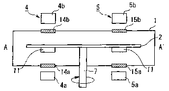
The film forming apparatus of the present embodiment is constructed as a
sputtering apparatus as is shown in Figures 1 through 3, this sputtering
apparatus
comprises a vacuum chamber 1 used as a film forming chamber, a rotating table
2
which is disposed inside the vacuum chamber 1, two sputtering sources 3 (only
one
of these is shown in the figures), and three optical monitors 4, 5 and 6.
The rotating table 2 is arranged so that this table can be caused to rotate
about a rotating shaft 7 by an actuator such as a motor, etc. (not shown in
the
figures). Substrates 11 that will constitute optical members 10, and a
monitoring
substrate 21, are attached via a holder (not shown in the figures) to the
undersurface of the rotating table 2 in respective positions on a concentric
circle
22
CA 02470959 2004-06-18
centered on the shaft 7. In the example shown in Figures 1 through 3, seven
substrates 11 and one monitoring substrate 2I are attached to the rotating
table 2.
The two sputtering sources 3 are respectively disposed in two locations in the
lower part of the vacuum chamber 1 which are such that these sputtering
sources 3
can face the substrates 11 and 21 as the rotating table 2 rotates. In the
present
embodiment, particles of components that constitute the layers fly from these
two
sputtering sources 3, and strike the surfaces of the substrates 11 and
monitoring
substrate 21, so that layers are formed. In the present embodiment, the target
materials are different in the two sputtering sources 3, so that the substance
with a
high refractive index and substance with a low refractive index (described
above)
respectively fly from the two sputtering sources 3.
For example, the monitoring substrate 21 consists of a transparent flat plate
such as a glass substrate. Since flat substrates are used as the substrates of
the
optical members 10 as described above, the same substrates are used as the
substrates 11 and monitoring substrate 21. The monitoring substrate 21 is a
dummy substrate used for film thickness measurement (i.e., a substrate that
does
not ultimately become an optical member 10)~ the thicknesses of the films that
are
formed on top of the substrates 11 under the same conditions are indirectly
measured by measuring the thickness of the film that is formed on the surface
of
this monitoring substrate 21. Depending on the case, it may not be absolutely
23
CA 02470959 2004-06-18
necessary to use such a monitoring substrate 21. However, in cases where the
surfaces of the optical members 10 are curved surfaces, as when the optical
members 10 are lenses, accurate measurement of the film thickness on such
surfaces is difficult accordingly, it is desirable to use a monitoring
substrate 21.
As is shown in Figures 2 and 3, three windows 14b, 15b and 16b are formed
in the upper surface of the vacuum chamber 1, and three windows 14a, 15a and
16a
are formed in the lower surface of the vacuum chamber 1. The pair of windows
14a
and 14b are disposed so that these windows are located on either side of a
specified
position through which the substrates 11 and 21 pass as the rotating table 2
rotates.
Another pair of windows 15a and 15b, as well as the other pair of windows 16a
and
16b, are also similarly disposed.
The optical monitor 4 is constructed from a light emitting device 4a and a
light receiving device 4b which splits and receives the light that is emitted
from the
light emitting device 4a and that passes through the window 14a, substrate 11
or
monitoring substrate 21, and window 14b~ this optical monitor 4 is arranged so
that
it can measure the spectroscopic transmissivity of the film formed on the
surface of
the substrate 11 or monitoring substrate 21. Similarly, the optical monitor 5
is
constructed from a light emitting device 5a and a light receiving device 5b
which
splits and receives the light that is emitted from the light emitting device
5a and
that passes through the window 15a, substrate 11 or monitoring substrate 21,
and
24
CA 02470959 2004-06-18
window 15b, and this optical monitor 5 is also arranged so that it can measure
the
spectroscopic transmissivity of the film formed on the surface of the
substrate 11 or
monitoring substrate 21. Similarly, the optical monitor 6 is constructed from
a light
emitting device 6a and a light receiving device 6b which splits and receives
the light
that is emitted from the light emitting device 6a and that passes through the
window 16a, substrate 11 or monitoring substrate 21, and window 16b, and this
optical monitor 6 is also arranged so that it can measure the spectroscopic
transmissivity of the film formed on the surface of the substrate 11 or
monitoring
substrate 21.
The optical monitor 4 is constructed so that it measures the spectroscopic
transmissivity in a specified wavelength region in the visible region, e.g.,
400 nm to
850 nm. The optical monitor 5 is constructed so that this optical monitor
measures
the spectroscopic transmissivity in a specified wavelength region in the
infrared
region, e.g., 1000 nm to 1700 nm. The optical monitor 6 is constructed so that
this
optical monitor measures the spectroscopic transmissivity in the actual-use
wavelength region of the optical members 10 (this corresponds to the
wavelength
region described as the "specified wavelength region in which the film is
used" in
the sections titled "Claims" and "Disclosure of the Invention"), e.g., 1520 nm
to
1570 nm. The respective optical monitors 4 through 6 are specially constructed
for
the respective measurement wavelength regions.
CA 02470959 2004-06-18
In the present embodiment, since the measurement wavelength region of the
optical monitor 5 includes the actual-use wavelength region of the optical
members
10, which is the measurement wavelength region of the optical monitor 6, the
actual-use wavelength region of the optical members 10 can also be measured by
the optical monitor 5. Accordingly, it would be possible to omit the optical
monitor 6
and to combine the function of the optical monitor 6 with the optical monitor
5.
However, if the optical monitors 5 and 6 are separately constructed as in the
present embodiment, the resolution of the optical monitor 6 can be increased
compared to the resolution of the optical monitor 5 since the measurement
wavelength region of the optical monitor 6 is narrower than the measurement
wavelength region of the optical monitor 5. Accordingly, the spectroscopic
transmissivity in the actual-use wavelength region can be measured with a high
resolution, which is advantageous. Conversely, in cases where the
spectroscopic
transmissivity in the actual-use wavelength region of the optical members 10
can be
used to determine the film thicknesses of the respective layers, it would be
possible
to omit the optical monitor 5 and to use the optical monitor 6 as a film
thickness
monitor as well.
In the following description, for the sake of convenience, the optical monitor
4
will be called the "visible region optical monitor," the optical monitor 5
will be called
the "film thickness measurement infrared monitor," and the optical monitor 6
will
be called the "actual-use wavelength region infrared monitor."
26
' CA 02470959 2004-06-18
As is shown in Figure 5, the film forming apparatus of the present
embodiment comprises a control and calculation processing part 17 constructed
from (for example) a computer, which controls the overall apparatus and
performs
specified calculations and the like in order to realize the operation
described below,
an operating part 18 which is used by the user to input instructions and data,
etc.,
into the control and calculation processing part 17, and a display part 19
such as a
CRT. The control and calculation processing part 17 has an internal memory 20.
Of course, it would also be possible to use an external memory instead of this
internal memory 20. Furthermore, like other universally known film forming
apparatuses, the film forming apparatus of the present embodiment also
comprises
a pump which is used to place the interior of the vacuum chamber 1 in a vacuum
state, a gas supply part which supplies specified gases to the interior of the
vacuum
chamber 1, and the like. However, a description of these parts is omitted.
Nest, one example of the operation of the film forming apparatus of the
present embodiment will be describe with reference to Figure 6. Figure 6 is a
schematic flow chart which shows one example of the operation of the film
forming
apparatus of the present embodiment.
27
CA 02470959 2004-06-18
Film formation is initiated in a state in which substrates 11 and a monitoring
substrate 21 on which no films have yet been formed are attached to the
rotating
table 2.
First, the user performs initial settings by operating the operating part 18
(step S1). In these initial settings, setting information is input which sets
the
measurement mode of the film thickness monitoring optical measurements
performed in step S4 described below as either the visible region measurement
mode (a mode in which film thickness monitoring optical measurements are
performed by the visible region optical monitor 4) or the infrared region
measurement mode (a mode in which film thickness monitoring optical
measurements are performed by the film thickness measurement infrared monitor
5). Furthermore, in these initial settings, the set film thickness values,
materials,
number of layers n, film formation conditions, and the like for the respective
layers
M1 through Mn are input which are such that the desired optical
characteristics of
the optical member 10 can be obtained, and which are predetermined according
to
advance design or the like.
Moreover, it would also be possible to provide the control and calculation
processing part 17 with a design function for the optical thin film 12 so that
when
the user inputs the desired optical characteristics, the control and
calculation
processing part 17 automatically determines the set film thickness values,
28
CA 02470959 2004-06-18
materials, nvtcnbP~~ of layers n, film formation conditions, and the like of
the
respective layers M1 through Mn in accordance with this design function.
Furthermore, in these initial settings, setting information indicating the
layer of
film formation at which the optical measurement of the actual-use wavelength
region is to be performed in step S6 (described later), etc., is also input.
For example, the selection of this layer may be set as all of the layers M1
through Mn, or may be set as only the uppermost layer Mn~ alternatively, the
selection may be set as the uppermost layer Mn and one or more other arbitrary
layers (e.g., at every specified number of layers). A setting may also be used
in
which no layer is selected, and the optical measurement of the actual-use
wavelength region in step S6 is not performed for any layer at the minimum,
however, it is desirable to select the uppermost layer Mn.
Next, the control and calculation processing part 17 sets a count value m
which indicates the number of the current layer as counted from the side of
the
substrate 11 at 1 (step S2).
Then, under the control of the control and calculation processing part 17, the
film formation of the mth layer is performed (e.g., by time control) on the
basis of
the set film thickness value and film formation conditions, etc., set for this
layer
(step S3). In the case of the first layer M1, film formation is performed on
the basis
29
CA 02470959 2004-06-18
of the set film thickness value that has been set in step S1. However, in the
case of
the second or subsequent layers, if the set film thickness value has been
adjusted in
step S9 (described later), film formation is performed on the basis of the
most
recently adjusted set film thickness value. During film formation, the
rotating table
2 is caused to rotate, and only the shutter (not shown in the figures)
disposed facing
the sputtering source 3 that corresponds to the material of the mth layer is
opened,
so that particles from this sputtering source 3 are deposited on the
respective
substrates 11 and monitoring substrate 21. When the film formation of the mth
layer is completed, this shutter is closed.
Subsequently, under the control of the control and calculation processing part
17, film thickness monitoring optical measurements are performed in the
measurement mode that has been set in step S1 (step S4).
In cases where the visible region measurement mode is set in step Sl, the
spectroscopic transmissivity of the monitoring substrate 21 or substrate 11 in
the
specified wavelength region within the visible region described above is
measured
by the visible region optical monitor 4 in step S4, and this data is stored in
the
memory 20 in association with the current count value m. Measurements by the
visible region optical monitor 4 are performed when the monitoring substrate
21 or
substrate 11 in question is positioned between the light emitting device 4a
and light
receiving device 4b in a state in which the rotating table 2 is rotating, or
are
CA 02470959 2004-06-18
performed with the rotating table 2 stopped in a state in which the monitoring
substrate 21 or substrate 11 is positioned between the light emitting device
4a and
light receiving device 4b.
On the other hand, in cases where the infrared region measurement mode is
set in step Sl, the spectroscopic transmissivity of the monitoring substrate
21 or
substrate 11 in the specified wavelength region within the infrared region
described
above is measured by the film thickness measurement infrared monitor 5, and
this
data is stored in the memory 20 in association with the current count value m.
Measurements by the film thickness measurement infrared monitor 5 are
performed when the monitoring substrate 2I or substrate 11 in question is
positioned between the light emitting device 5a and light receiving device 5b
in a
state in which the rotating table 2 is rotating, or are performed with the
rotating
table 2 stopped in a state in which the monitoring substrate 21 or substrate
1I is
positioned between the light emitting device 5a and light receiving device 5b.
l3asi.cally, in step S4, the spectroscopic transmissivity characteristics of
either
the monitoring substrate 21 or substrate 11 may be measured in either
measurement mode. Furthermore, for each layer, the spectroscopic
transmissivity
characteristics of either the monitoring substrate 21 or substrate 11 may be
arbitrarily set beforehand by the user as the spectroscopic transmissivity
characteristics that are measured.
31
CA 02470959 2004-06-18
When the film thickness monitoring optical measurements performed in step
S4 are completed, the control and calculation processing part 17 judges
whether or
not the actual-use wavelength region optical measurements of step S6 are to be
performed when film formation has been performed up to the current mth layer
(i.e., in the state in which the mth layer has been formed as the uppermost
layer)
(step S5), on the bases. of the setting information that has been set in step
S1. If it
is judged that the actual-use wavelength region optical measurements are not
to be
performed, the processing proceeds directly to step S7, while if it is judged
that the
actual-use wavelength region optical measurements are to be performed, the
processing proceeds to step S7 after passing through step S6.
In step S6, the spectroscopic transmissivity of the monitoring substrate 21 or
substrate 11 in the actual-use wavelength region described above is measured
by
the actual-use wavelength region infrared monitor 6, and this data is stored
in the
memory 20. Measurements by the actual-use wavelength region infrared monitor 6
are performed when the substrate 11 is positioned between the light emitting
device
6a and light receiving device 6b in a state in which the rotating table 2 is
rotating,
or are performed with the rotating table 2 stopped in a state in which the
substrate
11 is positioned between the light emitting device 6a and light receiving
device 6b.
32
CA 02470959 2004-06-18
In step S7, the control and calculation processing part 17 determines the film
thickness of the current mth layer on the basis of the spectroscopic
transmissivity
characteristics measured in step S6. Tn regard to the actual procedure that is
used
to determine the film thickness from the spectroscopic transmissivity
characteristics, various types of publicly known procedures, or fitting
similar to that
performed in steps S30 and S31 (shown in Figure 7 described later), may be
employed.
Next, the control and calculation processing part 1? judges whether or not
m = n, i.e., whether or not film formation has been completed up to the anal
layer
Mn (step S8). If this elm formation has not been completed, the set film
thickness
values for the layers from the (m+1)th layer on (i.e., the layers that have
not yet
been formed) are adjusted and optimized on the basis of the respective film
thicknesses determined in step S6 for each layer up to the mth layer so that
the
optical characteristics of the optical member 10 that will ultimately be
obtained are
adjusted to the desired optical characteristics (step S9). For example, such
optimization can be performed using various types of publicly known
procedures.
The set film thickness values for the layers from the (m+1)th layer on that
are
adjusted in this step S9 are used in step S3 when the layers from the (m+1)th
layer
on are formed. Following the adjustment performed in step S9, the count value
m of
the number of layers is increased by 1 (step S10), and the processing returns
to step
S3.
33
CA 02470959 2004-06-18
On the other hand, if it is judged in step S8 that film formation up to the
final
layer Mn has been completed, the spectroscopic transmissivity characteristics
in the
actual-use wavelength region measured in each step S6, and the film
thicknesses of
the respective layers determined in each step S7, which are stored in the
memory
20, are displayed on the display part 19 along with the associated count
values m
(information indicating which layer was formed as the uppermost layer at the
time
that the data was obtained), and if necessary, this data is output to an
external
personal computer, etc. (step S11)~ with this, the formation of the optical
thin film
12 on the substrate 11 is completed.
Optical members 10 can be manufactured in this manner.
Furthermore, on the basis of the film thicknesses of the respective layers and
the spectroscopic transmissivity characteristics in the actual-use wavelength
region
that are displayed or output in step 511, the user determines the set film
thickness
values and film formation conditions of the respective layers that are to be
set in
step S1 when the next optical thin film 12 is formed on the next substrate 11
(from
a comparison of the above data with the initial set film thickness values of
the
respective layers and desired optical characteristics of the optical member
10) so
that optical characteristics that axe closer to the desired optical
characteristics can
be obtained when the next optical thin film 12 is formed on the next substrate
11.
34
~
CA 02470959 2004-06-18
When the next optical thin film 12 is formed on the next substrate 11, the set
film
thickness values and film formation conditions of the respective layers thus
determined are set in step Sl.
Thus, in the present embodiment, feedback in which information that is
obtained when the optical thin film 12 is formed on the current substrate 11
is
reflected in the set film thickness values and film formation conditions for
the
respective layers that are set in step S1 when the next optical thin film 12
is formed
on the next substrate 11 can be performed via the user.
However, it is also possible to automate the processing by endowing the
control and calculation processing part 17 with such a feedback function. In
this
case, for example, a lookup table or the like which shows the correspondence
between the information that is obtained when the optical thin film 12 is
formed on
the current substrate 11 and the set film thickness values and film formation
conditions for the respective layers that are to be initially set when the
next optical
thin film 12 is formed on the next substrate 11 may be constructed beforehand,
and
the system may be constructed so that the control and calculation processing
part
17 performs the feedback described above by referring to this lookup table or
the
like.
CA 02470959 2004-06-18
The various advantages described below can be obtained in the present
embodiment.
To describe the first advantage, in the present embodiment, regardless of
which measurement mode is set as the measurement mode of the film thickness
monitoring optical measurements performed in step S4, if the layer that
determines
the timing of the measurement of the optical characteristics in the actual-use
wavelength region within the infrared region in step S6 is set as the
uppermost
layer Mn in step S1, the spectroscopic transmissivity characteristics (in the
actual-
use wavelength region within the infrared region) of the optical member 10
having
the entire optical thin film 12 finally formed are measured in step S6~
accordingly,
feedback can be performed in which this information is reflected in the film
formation of the next optical thin film 12 on the next substrate 11.
Consequently,
an optical thin film 12 which has desired optical characteristics that are
more
accurately reproduced can be obtained. In particular, if the layer that
determines
the timing of the measurement of the optical characteristics in the actual-use
wavelength region is set not only as the uppermost layer Mn, but also as one
or
more other layers, the spectroscopic transmissivity characteristics in the
actual-use
wavelength region in a stage in which the film has been formed up to the point
of an
intermediate layer are also measured, and feedback can be performed in which
this
information is also reflected in the film formation of the next optical thin
film 12 on
the next substrate 11.
36
CA 02470959 2004-06-18
In this case, an optical thin film 12 which has desired optical
characteristics
that are reproduced much more accurately can be obtained. Furthermore, in the
present embodiment, since an actual-use wavelength region infrared monitor 6
is
installed separately from the film thickness measurement infrared monitor 5,
the
characteristics in the actual-use wavelength region can be measured with an
extremely high resolution. Accordingly, this is advantageous in that an
optical thin
film 12 which has desired optical characteristics that can be reproduced much
more
accurately can be obtained from this standpoint as well.
On the other hand, in a conventional film forming apparatus, since only a
visible region optical characteristic monitor is mounted, the optical
characteristics
of the optical member 10 in the actual-use wavelength region within the
infrared
region cannot be measured, so that the feedback of information in the actual-
use
wavelength region as described above is completely impossible.
Secondly, in the present embodiment, if the measurement mode of the film
thickness monitoring optical measurements that are performed in step S4 is set
as
the infrared region measurement mode, then the film thickness monitoring
optical
measurements are performed by the film thickness monitoring infrared monitor 5
as described above, and the film thicknesses of the respective layers are
determined
from the spectroscopic characteristics in the infrared region obtained by
these
37
CA 02470959 2004-06-18
measurements. Since the wavelengths in the infrared region are longer than the
wavelengths in the visible region, a large and abrupt repetitive variation
with
respect to changes in wavelength is less likely to appear in the infrared
region than
in the visible region, even if the total film thickness or number of layers
formed is
large.
Accordingly, in the present embodiment, if the measurement mode is set as
the infrared region measurement mode, even if the total film thickness or
number of
layers formed is large, the film thicknesses of the respective layers can be
determined with greater precision than in cases where the film thicknesses of
the
respective layers are determined from the spectroscopic characteristics in the
visible
region as in a conventional film forming apparatus consequently, it is
possible to
obtain an optical thin film 12 with desired optical characteristics that are
accurately
reproduced. Thus, since the film thicknesses of the respective layers can be
precisely measured in cases where the measurement mode is set as the infrared
region measurement mode even if the total film thickness or number of layers
formed is large, the need to replace the monitoring substrate 21 during film
formation can be completely eliminated, or the frequency of such replacement
can
be reduced even if the total film thickness of the optical thin film 12 is
large
consequently, the productivity is greatly improved.
38
CA 02470959 2004-06-18
In cases where the need to replace the monitoring substrate 21 is completely
eliminated, if the substrate 11 that constitutes the optical member 10 is (for
example) a flat plate, the spectroscopic characteristics of the substrate 11
may be
measured by the film thickness monitoring infrared monitor 5. In this case,
since
there is no need to use a monitoring substrate, the productivity can be
further
improved.
Thirdly, in the present embodiment, if the measurement mode of the film
thickness monitoring optical measurements that are performed in step S4 is set
as
the visible region measurement mode, then the film thickness monitoring
optical
measurements are performed by the visible region monitor 4 as described above,
and the film thicknesses of the respective layers are determined from the
spectroscopic characteristics in the visible region obtained by these
measurements.
Accordingly, in cases where the total film thickness or number of layers of
the
optical thin film 12 is large, the monitoring substrate 21 must be replaced
during
film formation as in a conventional film forming apparatus in order to obtain
the
film thicknesses of the respective layers with good precision. Consequently,
this
embodiment of the film forming apparatus of the present invention is
comparable to
a conventional film forming apparatus in terms of productivity. However, since
the
wavelengths in the visible region are shorter than the wavelengths in the
infrared
region, the spectroscopic characteristics in the visible region can be
measured with
39
CA 02470959 2004-06-18
good sensitivity compared to the spectroscopic characteristics in the infrared
region
in cases where the total film thickness or number of layers formed is small.
Accordingly, if the measurement mode is set as the visible region
measurement mode, although the productivity is inferior to that obtained when
the
measurement mode is set as the infrared region measurement mode in cases where
the total film thickness or number of layers of the optical thin film 12 is
large, the
film thicknesses of the respective layers can be obtained with greater
precision, so
that an optical thin film 12 which has desired optical characteristics that
can be
reproduced with greater accuracy can be obtained. Of course, this advantage
that is
obtained in case where the measurement mode is set as the visible region
measurement mode is an advantage that is also obtained in the conventional
film
forming apparatus described above. However, in the visible region measurement
mode of the present embodiment, this advantage is obtained simultaneously with
the first advantage describe above accordingly, the technical significance of
this
advantage is extremely high.
Second Embodiment]
Figures 7 and 8 are schematic flow charts which illustrate the operation of a
film forming apparatus constituting a second embodiment of the present
invention.
CA 02470959 2004-06-18
The film forming apparatus constituting the present embodiment differs from
the film forming apparatus constituting the first embodiment described above
only
in the following respect: namely, in the first embodiment described above, the
control and calculation processing part 17 is constructed so that the
operation
shown in Figure 6 described above is realized, while in the present
embodiment, the
control and calculation processing part 17 is constructed so that the
operation
shown in Figures 7 and 8 is realized. In all other respects, the film forming
apparatus of the present embodiment is the same as that of the first
embodiment
described above. Here, therefore, the operation shown in Figures 7 and 8 will
be
described since other descriptions are redundant, such other descriptions will
be
omitted.
Film formation is initiated in a state in which the substrates 11 and
monitoring substrate 21 on which no films have yet been formed are attached to
the
rotating table 2.
First, the user performs initial settings by operating the operating part 18
(step S21). In these initial settings, setting information indicating whether
the film
thickness determination mode is set as the mode using one wavelength region or
the mode using both wavelength regions is input. Here, the term "film
thickness
determination mode" refers to the system used to determine the film thickness
of
the layer formed as the uppermost Iayer at the point in time in question.
41
CA 02470959 2004-06-18
Furthermore, the term "mode using one wavelength region" refers to a system in
which the film thickness of this layer is determined with only one type of
spectroscopic transmissivity value among the spectroscopic transmissivity
values '
measured by the visible region optical monitor 4 and the spectroscopic
transmissivity values measured by the film thickness measurement infrared
monitor 5 being selectively used as the measurement data. Moreover, the term
"mode using both wavelength regions" refers to a system in which the film
thickness
of this layer is determined using both the spectroscopic transmissivity values
measured by the visible region optical monitor 4 and the spectroscopic
transmissivity values measured by the film thickness measurement infrared
monitor 5. Furthermore, the same film thickness determination mode is used for
all
of the layers M1 through Mn.
Furthermore, in the initial settings in step 521, a tolerance Ti corresponding
to each of the layer numbers m is set which is used in the mode using both
wavelength regions. This point will be described in detail later.
Furthermore, in the initial settings in step 521, the set film thickness
values,
materials, numbers of layers n, film formation conditions, and the like for
the
respective layers M1 through Mn are input which are such that the desired
optical
characteristics of the optical member 10 can be obtained, and which are
predetermined according to advance design or the like. Moreover, it would also
be
42
CA 02470959 2004-06-18
possible to provide the control and calculation processing part 1'7 with a
design
function for the optical thin film 12 so that the control and calculation
processing
part 17 automatically determines the set film thickness values, materials,
numbers
of layers n, film formation conditions, and the like for the respective layers
M1
through Mn by means of this design function when the user inputs the desired
optical characteristics.
Furthermore, in the initial settings in step 521, setting information
indicating the layer of film formation at which the actual-use wavelength
region
optical measurements of step S27 (described later) are to be performed (and
the
like) is also input. In the selection of this layer, for example, one or more
arbitrary
layers other than the uppermost layer Mn (e.g., layers separated by a
specified
number of layers) may be selected, the uppermost layer Mn and one or more
other
arbitrary layers may be selected, or all of the layers M 1 through Mn may be
selected.
Furthermore, the uppermost layer Mn alone may be selected, or a setting may be
used in which no layer is selected, so that the actual-use wavelength region
optical
measurements of step S27 are not performed for any of the layers. However, it
is
desirable to select at least one layer other than the uppermost layer Mn.
Next, the control and calculation processing part 17 sets a count value m
which indicates the number of the current layer (i.e., the layer number) as
counted
from the side of the substrate 11 at 1 (step S22).
43
CA 02470959 2004-06-18
Next, under the control of the control and calculation processing part 17, the
film formation of the mth layer is performed (for example) using time control
on the
basis of the set film thickness values and film formation conditions, etc.,
that were
set for this layer (step S23). In the case of the first layer M1, the layer is
formed on
the basis of the set film thickness value that was set in step 521 however, in
the
case of layers from the second layer on, if the set film thickness value has
been
adjusted in step S39 (described later), the layer is formed on the basis of
the most
recently adjusted set film thickness value. During film formation, the
rotating table
2 is caused to rotate, and only the shutter (not shown in the figures)
installed facing
the sputtering source 3 corresponding to the material of the mth layer is
opened, so
that particles from this sputtering source 3 are deposited on the respective
substrates 11 and monitoring substrate 21. When the film formation of the mth
layer is completed, this shutter is closed.
Subsequently, under the control of the control and calculation processing part
17, the spectroscopic transmissivity of the monitoring substrate 21 or
substrates 11
in the specified wavelength region within the visible region described above
is
measured by the visible region optical monitor 4, and this data is stored in
the
memory 20 in association with the current count value m (step S24). The
measurements performed by the visible region optical monitor 4 are performed
when the monitoring substrate 21 or substrate 11 in question is positioned
between
44
CA 02470959 2004-06-18
the light emitting device 4a and light receiving device 4b in a state in which
the
rotating table 2 is rotating, or with the rotating table 2 stopped in a state
in which
the monitoring substrate 21 or substrate 11 is positioned between the light
emitting
device 4a and light receiving device 4b.
Next, under the control of the control and calculation processing part 17, the
spectroscopic transmissivity of the monitoring substrate 21 or substrate 11 in
question in the specified wavelength region within the infrared region
described
above is measured by the film thickness measurement infrared monitor 5, and
this
data is stored in the memory 20 in association with the current count value m
(step
S25). The measurements performed by the film thickness measurement infrared
monitor 5 are performed when the monitoring substrate 21 or substrate 11 in
question is positioned between the light emitting device 5a and light
receiving
device 5b in a state in which the rotating table 2 is rotating, or with the
rotating
table 2 stopped in a state in which the monitoring substrate 21 or substrate
11 is
positioned between the light emitting device 5a and light receiving device 5b.
Next, on the basis of the setting information set in step 521, the control and
calculation processing part 17 judges whether or not the actual-use wavelength
region optical measurements of step S27 are to be performed at the point in
time at
which film formation has been performed up to the current mth layer (i.e., in
a state
in which the mth layer has been formed as the uppermost layer) (step S26). If
it is
CA 02470959 2004-06-18
judged that the actual-use wavelength region optical measurements are not to
be
performed, the processing proceeds directly to step 528 if it is judged that
the
actual-use wavelength region optical measurements are to be performed, the
processing proceeds to step S28 after passing through step 527.
In step 527, the spectroscopic transmissivity of the monitoring substrate 21
or substrate 11 in the actual-use wavelength region described above is
measured by
the actual-use wavelength region infrared monitor 6, and this data is stored
in the
memory 20. The measurements performed by the actual-use wavelength region
infrared monitor 6 are performed when the substrate 11 in question is
positioned
between the light emitting device 6a and light receiving device 6b in a state
in
which the rotating table 2 is rotating, or with the rotating table 2 stopped
in a state
in which the substrate 11 is positioned between the light emitting device 6a
and
Iight receiving device 6b.
In step 528, the control and calculation processing part 17 judges whether
the film thickness determination mode set in step S21 is the mode using one
wavelength region or the mode using both wavelength regions. If this mode is
the
mode using one wavelength region, the processing proceeds to step 529 if the
mode
is the mode using both wavelength regions, the processing proceeds to step
532.
46
CA 02470959 2004-06-18
In step 529, the control and calculation processing part 1'7 judges whether or
not the total film thickness of the layers from the first through mth layers
is less
than 10 Vim. However, since the film thickness of the mth layer has not yet
been
determined at this point in time, the judgement of step S29 is performed with
the
sum of the respective film thicknesses of the layers from the first through (m-
1)th
layers that have already been determined in step S30 or step S31 and the set
film
thickness value for the mth layer taken as the total film thickness of the
layers from
the first through mth layers.
The judgement reference value used in step S29 is not limited to 10 ~m~ it is
desirable to set this value as a specified value in the range of 1 ~m to 10
~,m, and it
is even more desirable to set this value as a specified value in the range of
6 ~,m to
Vim. The reasons for setting these values has already been described. Instead
of
judging the total film thickness in step 529, it would also be possible to
judge the
number of layers that have been formed up to the current time (i.e., the count
value).
In cases where a judgement is made on the basis of the number of layers, the
approximate total film thickness can be calculated from the number of layers
since
the film thickness per layer shows no great variation.
Accordingly, a procedure in which the number of layers that produces a
specified total film thickness is calculated, and the judgement reference
value in
step S29 is set on the basis of this number of layers, is also included in the
scope of
47
CA 02470959 2004-06-18
the present invention. If the total film thickness is less than 10 Vim, the
processing
proceeds to step 530, and if the total film thickness is ZO ~m or greater, the
processing proceeds to step 531.
In step 530, the control and calculation processing part 1? determines the
film thickness of the mth layer using only the spectroscopic transmissivity in
the
visible region measured in step 524, without using the spectroscopic
transmissivity
in the infrared region measured in step 525, by fitting the corresponding
spectroscopic transmissivity calculated with the thickness of the mth layer
assumed
as various values to this measured spectroscopic transmissivity in the visible
region.
Here, the corresponding spectroscopic transmissivity is the spectroscopic
transmissivity of a multi-layer film model (thin film model) comprising layers
from
the first through mth layers. In the calculation of the spectroscopic
transmissivity
of this multi-layer film model, the film thicknesses that have already been
determined in step S30 or step S31 axe used as the respective film thicknesses
of
the layers from the first through (m-1)th layers. When step S30 is completed,
the
processing proceeds to step 534.
Here, one example of the spectroscopic transmissivity in the infrared region
measured in step S25 is shown as the measured transmissivity in Figure 9.
Furthermore, the spectroscopic transmissivity calculated with the film
thickness of
48
CA 02470959 2004-06-18
the uppermost layer assumed to be a certain thickness (corresponding to the
measured transmissivity) is shown as the calculated transmissivity in Figure
9. In
the example shown in Figure 9, since the assumed film thicknesses show a
considerable deviation from the actual film thicknesses, there is a
considerable
deviation between the measured spectroscopic transmissivity and the calculated
spectroscopic transmissivity.
In the fitting of the calculated spectroscopic transmissivity to the measured
spectroscopic transmissivity, an evaluation value which evaluates the
deviation
between the respective values (or conversely, the degree of fitting) is
calculated.
This evaluation value is calculated for each film thickness with the film
thickness of
the mth layer assumed as various values. Furthermore, the film thickness that
is
assumed when the evaluation value (among all of the evaluation values) that
shows
the smallest deviation (the minimum value in the case of the merit value MF
described later) is calculated is determined to be the film thickness of the
mth layer.
This is the concrete content of the fitting processing.
In the present embodiment, a merit value MF based on a merit function is
used as the evaluation value that is used in the fitting of step 530. Of
course, it
goes without saying that evaluation values that can be used are not limited to
such
a merit value MF. The definition of this merit value MF is shown in the
following
Equation (1).
49
CA 02470959 2004-06-18
T! ~t arget - ~calc
MF = 1 ~ t
~( N ,_, T
In Equation (1), N is the total number of targets (total number of
transmissivity values at respective wavelengths in the measured transmissivity
characteristics). i is a number corresponding to the wavelength in a one-to-
one
correspondence, and is a number that is attached to quantities relating to a
certain
wavelength. This number may have any value from 1 to N. Qtarget is the
transmissivity value in the measured transmissivity characteristics. (~~ai~ is
the
transmissivity value in the calculated transmissivity characteristics. T is
the
tolerance (the reciprocal of this value is generally called the weighting
factor).
When Equation (1) is applied in step 530, fatargetl through QtargecN In
Equation (1) are the transmissivity values in the spectroscopic transmissivity
in the
visible region measured in step 524. Furthermore, in the present embodiment,
in
cases where the merit value MF is used in step 530, the tolerance values Ti (i
is 1
through N) are all set at l, and none of the data of the respective
transmissivity
values is weighted, so that these sets of data are all treated equally.
Referring again to Figure 7, in step 531, the control and calculation
processing part 1'7 determines the film thickness of the mth layer using only
the
CA 02470959 2004-06-18
spectroscopic transmissivity in the infrared region measured in step 525,
without
using the spectroscopic transmissivity in the visible region measured in step
524, by
fitting the corresponding spectroscopic transmissivity that is calculated with
the
thickness of the mth layer assumed as various values to this measured
spectroscopic transmissivity in the infrared region. In the present
embodiment, the
processing of step S31 is the same processing as the processing of step 530,
except
for the fact that the spectroscopic transmissivity in the infrared region
measured in
step S25 is used instead of the spectroscopic transmissivity in the visible
region
measured in step 524. When Equation (1) is applied in step 531, ~targeci
through
(atargetN In Equation (I) are the transmissivity values in the spectroscopic
transmissivity in the infrared region measured in step 525. When step S31 is
completed, the processing proceeds to step 534.
In cases where the film thickness determination mode set in step S21 is the
mode using both wavelength regions, the control and calculation processing
part 17,
in step 532, determines the tolerance Ti corresponding to the current layer
number
m (this layer number m indicates the number of layers currently formed) from
the
tolerances set in step 521.
Subsequently, in step 533, the control and calculation processing part 1'7
determines the film thickness of the mth layer using the overall spectroscopic
transmissivity that combines both the spectroscopic transmissivity in the
visible
51
CA 02470959 2004-06-18
region measured in step S24 and the spectroscopic transmissivity in the
infrared
region measured in step 525, by fitting the corresponding spectroscopic
transmissivity calculated with the thickness of the mth layer assumed as
various
values to this measured overall spectroscopic transmissivity. When step S33 is
completed, the processing proceeds to step 534.
In the present embodiment, the merit value MF is used as the evaluation
value in the fitting of step S33 as well. When Equation (1) is applied in step
533,
(atargetl through QtargetN In Equation (1) are the transmissivity values in
the
spectroscopic transmissivity in the visible region measured in step S24 and
the
transmissivity values in the spectroscopic transmissivity in the infrared
region
measuxed in step 525.
In steps S30 and 531, the tolerance values Ti (i is 1 through N) were all set
at
1, so that none of the data of the respective transmissivity values was
weighted. In
step 533, on the other hand, the tolerance values Ti determined in step S32
are
used, and the data of the respective transmissivity values is weighted by
appropriately setting the tolerance Ti for each of the layer numbers m in step
521.
In the present embodiment, in cases where the number of layers m currently
formed
is equal to or less than a specified number of layers, the tolerance Ti for
each of the
number of layers m is set in step S21 so that fitting is performed in step S33
with a
greater emphasis on the spectroscopic transmissivity in the visible region
measured
52
CA 02470959 2004-06-18
in step S24 than on the spectroscopic transmissivity in the infrared region
measured in step 525, and in cases where the number of layers m currently
formed
is greater than this specified number of layers, the tolerance Ti for each of
the
number of layers m is set in step S21 so that fitting is performed in step S33
with a
greater emphasis on the spectroscopic transmissivity in the infrared region
measured in step S25 than on the spectroscopic transmissivity in the visible
region
measured in step 524. Here, the term "emphasis" refers to weighting of the
data of
the evaluation value described above. In cases where the evaluation value is
the
merit value MF, this refers to a relative reduction of the tolerance.
Here, a concrete example of the setting of the tolerance Ti for each of the
number of layers m in step S21 will be described in combination with a
description
of the significance of the tolerance setting.
In the concrete example described below, the wavelength range of the overall
transmissivity characteristics obtained by the visible region optical monitor
4 and
film thickness measurement infrared monitor 5 is 400 nm to 1750 nm. The
tolerance in the merit function (Equation (1)) that is used when the film
thickness is
determined by fitting to the transmissivity characteristics thus obtained is
positively controlled. Since the tolerance can be set for the transmissivity
characteristics values at each wavelength, relative reduction of the tolerance
means
that it is desired to increase the degree of fitting to the measured value of
the
53
CA 02470959 2004-06-18
transmissivity at the wavelength in question. Conversely, a relative increase
in the
tolerance means that the degree of fitting to the measured value of the
transmissivity at the wavelength in question may be relatively poor.
For example, in cases where the total film thickness of the multi-layer film
on
the monitoring substrate 21 or substrate 14 is not very large, the visible
region
transmissivity characteristics obtained by the visible region optical monitor
4 are
emphasized accordingly, the tolerance in the visible region is reduced to a
tolerance
that is smaller than the tolerance in the infrared region. As the total film
thickness
of the multi-layer film on the monitoring substrate 21 or substrate 14
increases, the
tolerance in the visible region is increased, and the tolerance in the
infrared region
is reduced. By proceeding in this way, it is possible to suppress the error
that is
caused mainly by the resolution of the optical monitor, so that film formation
can be
continued without causing a drop in the precision of film thickness
determination.
Values that varied linearly with wavelength were used as the set tolerance
values in a case where a 41-layer film in which the thicknesses of all of the
layers
were more or less the same was actually formed on the monitoring substrate 21
(the
layer film thickness was approximately 15 microns). The tolerance settings for
the
first layer, fifteenth layer and fortieth layer are shown in Figures 10, 11
and 12,
respectively. Furthermore, the tolerance setting for the layer number at a
54
CA 02470959 2004-06-18
wavelength of 550 nm is shown in Figure 13, and the tolerance setting for the
layer
number at a wavelength of 1600 nm is shown in Figure 14.
Figure 15 is a diagram in which these tolerance settings are shown
comprehensively in three dimensions. By varying the first-order slope of the
tolerance vs. wavelength as the layers progress, it is possible to change from
an
emphasis on the visible region transmissivity characteristics to an emphasis
on the
infrared region transmissivity characteristics in the determination of the
film
thickness as the total film thickness of the multi-layer film on the
monitoring
substrate 21 increases. The linear variation of the tolerance shown here is
merely
one example in regard to the manner of this variation, it goes without saying
that
the tolerance can be varied in the most appropriate form in accordance with
the film
construction of the multi-layer film and the conditions of the optical
monitors, etc.
Returning again to the description in the flow chart, the control and
calculation processing part 1'7 judges in step S34 whether or not the actual-
use
wavelength region optical measurements of step S27 have already been performed
at the time that the film was formed up to the current mth layer (i.e., in a
state in
which the mth layer was formed as the uppermost layer). In cases where the
actual-use wavelength region optical measurements have been performed, the
processing proceeds to step 535 in cases where the actual-use wavelength
region
optical measurements have not been performed, the processing proceeds to step
538.
CA 02470959 2004-06-18
In step 535, the control and calculation processing part 17 calculates the
evaluation value of the deviation between the spectroscopic transmissivity in
the
actual-use wavelength region measured in step S27 and the corresponding
spectroscopic transmissivity that has been calculated. Here, the corresponding
spectroscopic transmissivity is the spectroscopic transmissivity of a multi-
layer film
model (thin film model) comprising layers from the first through mth layers.
In the
calculation of the spectroscopic transmissivity of this multi-layer film
model, the
film thicknesses already determined in steps 530, S31 or S33 are used as the
respective film thicknesses of the layers from the first through mth layers.
For example, the merit value MF can be used as the evaluation value that is
calculated in step 535. In cases where the merit value MF is used as this
evaluation value, since weighting has no particular meaning, the tolerance
values
Ti (i is 1 through N) may all be set at 1. When Equation (1) is applied in
step S34,
(atargetl through QtargetN In Equation (1) are the transmissivity values in
the
spectroscopic transmissivity in the actual-use wavelength region measured in
step
527.
Subsequently, the control and calculation processing part 17 judges whether
or not the evaluation value calculated in step S35 is within the permissible
range
(step S36). If this value is within the permissible range, the processing
proceeds to
56
CA 02470959 2004-06-18
step 538. On the other hand, if this value is not within the permissible
range, the
spectroscopic transmissivity characteristics in the actual-use wavelength
region
measured in each step 527, and the film thicknesses of the respective layers
determined in each step 530, S31 and 533, which are stored in the memory 20,
are
displayed on the display part 19 along with the associated count values m
(information indicating which layer was formed as the uppermost layer at the
time
of this data). If necessary, furthermore, this data is output to an external
personal
computer or the like (step S37), and film formation is stopped. Accordingly,
even if
the mth layer is an intermediate layer, the film formation of the layers from
the
(m+1)th layer on is not performed.
In cases where film formation is thus stopped at an intermediate point, the
user appropriately adjusts (for example) the refractive index dispersion data
constituting one of the conditions of the multi-layer film model calculated in
steps
530, S31 and 533, and forms the next optical thin film 12 on the next
substrate 11.
In step 538, the control and calculation processing part 17 judges whether or
not m = n, i.e., whether or not film formation has been completed up to the
final
layer Mn. If this film formation has not been completed, the set film
thickness
values of the layers from the (m+1)th layer on (layers that have not yet been
formed) are adjusted and optimized on the basis of the respective film
thicknesses of
the layers up to the mth layer determined in steps 530, S31 or S33 for each
layer so
57
CA 02470959 2004-06-18
that the optical characteristics of the optical member 10 that is ultimately
obtained
are the desired optical characteristics (step S39). For example, such
optimization
can be accomplished using various universally known procedures. The set film
thickness values of the layers from the (m+1)th layer on that are adjusted in
step
S39 are used in step S23 in the film formation of the layers from the (m+1)th
layer
on. Following the adjustment of step 539, the count value m of the number of
layers
is increased by 1 (step S40), and the processing returns to step 523.
On the other hand, in cases where it is judged in step S38 that film formation
has been completed up to the final layer Mn, the formation of the optical thin
film
12 on the substrate 11 in question is completed after processing similar to
that of
step S37 is performed in step 541.
An optical member 10 can be manufactured in this manner.
In the present embodiment, advantages similar to those of the first
embodiment are obtained in addition, the following advantages can also be
obtained:
In the present embodiment, in the case of mode using one wavelength region,
the film thicknesses of the respective layers are determined on the basis of
the
spectroscopic transmissivity in the visible region measured by the visible
region
58
CA 02470959 2004-06-18
optical monitor 4 when the total film thickness is less than 10 Vim, and are
determined on the basis of the spectroscopic transmissivity in the infrared
region
measured by the film thickness measurement infrared monitor 5 when the total
film thickness is 10 ~m or greater. Since the wavelengths in the infrared
region are
longer than the wavelengths in the visible region, a large and abrupt
repetitive
variation with respect to changes in wavelength is less likely to appear in
the
infrared region than in the visible region even if the total film thickness or
number
of layers formed is large. Accordingly, in the present embodiment, if the
measurement mode is set as the infrared region measurement mode, the film
thicknesses of the respective layers can be determined with greater precision
than
is possible in cases where the film thicknesses of the respective layers are
determined from the spectroscopic characteristics in the visible region as in
a
conventional film forming apparatus, even if the total film thickness or
number of
layers formed is large. Consequently, an optical thin film 12 with desired
optical
characteristics that are accurately reproduced can be obtained. Thus, since
the film
thicknesses of the respective layers can be precisely measured even if the
total film
thickness or number of layers formed is large, the need to replace the
monitoring
substrate 21 during film formation can be completely eliminated, or the
frequency of
such replacement can be reduced even if the total film thickness of the
optical thin
film 12 is large consequently, the productivity can be greatly improved. In
cases
where the need to replace the monitoring substrate 21 is completely
eliminated, the
spectroscopic characteristics of the substrate 11 that constitutes the optical
member
59
CA 02470959 2004-06-18
can also be measured by means of the film thickness monitoring infrared
monitor
5 if this substrate 11 is (for example) a flat plate. In this case, there is
no need to
use a monitoring substrate 11 ~ accordingly, the productivity can be increased
even
further.
Furthermore, in the present embodiment, in the case of the mode using both
wavelength regions, fitting is performed with a greater emphasis on the
spectroscopic transmissivity in the visible region measured by the visible
region
optical monitor 4 than on the spectroscopic transmissivity measured by the
film
thickness measurement infrared monitor 5 in cases where the number of layers
formed is equal to or less than a specified number of layers, and fitting is
performed
with a greater emphasis on the spectroscopic transmissivity measured by the
film
thickness measurement infrared monitor 5 than on the spectroscopic
transmissivity
measured by the visible region optical monitor 4 in cases where the number of
layers formed is greater than this specified number of layers.
Accordingly, advantages that are basically the same as those obtained in the
case of the mode using one wavelength region are also obtained in the case of
the
mode using both wavelength regions. In the case of the mode using both
wavelength regions, unlike the case of the mode using one wavelength region,
there
is no complete switching between the use of the spectroscopic transmissivity
in the
visible region and the use of the spectroscopic transmissivity in the infrared
region
CA 02470959 2004-06-18
instead, the contributions of both regions can be freely varied by
appropriately
setting the tolerance. Accordingly, the film thicknesses can be determined
with
higher precision in the case of the mode using both wavelength regions than in
the
case of the mode using one wavelength region.
Furthermore, in the present embodiment, the processing of steps S35 and
S36 is performed, and in cases where the evaluation value of the deviation
between
the spectroscopic transmissivity in the actual-use wavelength region and the
corresponding spectroscopic transmissivity that is calculated is outside a
permissible range, film formation is performed only up to an intermediate
layer,
and the film formation of the remaining layers is stopped. Accordingly, in the
present embodiment, a check can be made at an intermediate stage in the film
formation of the multi-layer film in order to ascertain if the performance of
the
optical multi-layer film that will ultimately be obtained has no prospect of
satisfying the performance requirements. In cases where there is no prospect
that
these requirements will be satisfied, the wasteful formation of the remaining
layers
up to the final layer can be avoided. Accordingly, the production efficiency
can be
greatly improved by using the present invention.
Respective embodiments of the present invention were described above.
However, the present invention is not limited to these embodiments.
61
CA 02470959 2004-06-18
For example, it would also be possible to modify the first embodiment so that
only the infrared measurement mode described above is always performed. In
this
case, the visible region optical monitor 4 can be eliminated.
Furthermore, it would also be possible to modify the first embodiment so that
only the visible region measurement mode described above is always performed.
In
this case, the film thickness monitoring infrared monitor 5 can be eliminated.
Moreover it would also be possible to modify the second embodiment so that
only the mode using one wavelength region or only the mode using both
wavelength
regions is always performed.
Furthermore, in the second embodiment, it would also be possible to devise
the system so that tolerance values Ti are set for respective total film
thicknesses in
step S21 in Figure 7, and the tolerance value Ti corresponding to the total
film
thickness is determined in step 532.
In addition, in the first and second embodiments, the optical monitors 4
through 6 were all monitors that measure the spectroscopic transmissivity.
However, at least one of the optical monitors 4 through 6 may be an optical
monitor
that measures the spectroscopic reflectivity.
62
CA 02470959 2004-06-18
Furthermore, the first and second embodiments were examples of a
sputtering apparatus. However, the present invention may also be applied to
other
film forming apparatuses such as vacuum evaporation apparatuses.
Industrial Applicability
The film forming apparatus of the present invention can be used to form
optical thin films and the like. Furthermore, the optical member manufacturing
method of the present invention can be used to manufacture optical members
that
have optical thin films.
63