Note: Descriptions are shown in the official language in which they were submitted.
CA 02471701 2004-06-25
WO 03/056538 PCT/CA02/02008
ENERGY EFFICIENT GREY SCALE DRIVER FOR ELECTROLUMINESCENT
DISPLAYS
FIELD OF THE INVENTION
The present invention relates generally to flat panel displays, and more
particularly to a resonant switching panel driving circuit where the panel
imposes a
variable high capacitive load on the driving circuit and where the driving
voltage
must be regulated to facilitate gray scale control.
BRIEF DESCRIPTION OF THE DRAWINGS
The Background of the Invention and Detailed Description of the Preferred
Embodiment are set forth herein below with reference to the following
drawings, in
which:
Fig. 1 is a plan view of an arrangement of rows and columns of pixels on an
electroluminescent display, in accordance with the Prior Art;
Fig. 2 is a cross section through a single pixel of the electroluminescent
display of Figure 1;
Fig. 3 is-an equivalent circuit for the pixel of Figure 2;
Fig. 4 is a simplified circuit schematic of a resonant circuit used in the
display
driver according to Applicant's earlier filed U.S. Patent Application No.
091504,472;
Figs. 5A - 5C are oscilloscope tracings that show waveforms for the resonant
circuit of Figure 4 under different conditions;
Fig. 6 is a simplified schematic of a transformer-'.secondary side portion of
a
display driver incorporating the elements of the present invention;
Fig. 7 is a block diagram of a driver circuit incorporating the elements of
the
present invention;
Fig. 8 is a detailed circuit diagram of a column driver according to the
preferred embodiment of the present invention;
Fig. 9 is a detailed circuit diagram of a row driver according to the
preferred
CA 02471701 2004-06-25
WO 03/056538 PCT/CA02/02008
2
embodiment of the present invention;
Fig. 10 is a detailed circuit diagram of a polarity reversing circuit employed
at
the output of the row driver of Figure 9; and
Fig. 11 and Fig. 12 are timing diagrams showing display timing pulses used in
the display driver of the present invention.
BACKGROUND OF THE INVENTION
Electroluminescent displays are advantageous by virtue of their low operating
voltage with respect to cathode ray tubes, their superior image quality, wide
viewing
angle and fast response time over liquid crystal displays, and their superior
gray
scale capability and thinner profile than plasma display panels. They do have
relatively high power consumption, however, due to the inefficiencies of pixel
charging, as discussed in greater detail below. This is the case even though
the
conversion of electrical energy to light within the pixels is relatively
efficient.
However, the disadvantage of high power consumption associated with
electroluminescent displays can be mitigated if the capacitive energy stored
in the
electroluminescent pixels is efficiently recovered.
The present invention relates to energy efficient methods and circuits for
driving display panels where the panel imposes a variable capacitive load on
the
driving circuit and where the driving voltage must be regulated to facilitate
gray scale
control. The invention is particularly useful for electroluminescent displays
where
the panel capacitance is high. The panel capacitance is the capacitance as
seen on
the row and column pins of the display. Electroluminescent display pixels have
the
characteristic that the pixel luminance is zero if the voltage across the
pixel is below
a defined threshold voltage, and becomes progressively greater as the voltage
is
increased beyond the threshold voltage. This property facilitates the use of
matrix
addressing to generate a video image on the display panel.
As shown in Figures 1 and 2, an electroluminescent display has two
intersecting sets of parallel electrically conductive address lines called
rows (ROW 1,
CA 02471701 2004-06-25
WO 03/056538 PCT/CA02/02008
3
ROW 2, etc.) and columns (COL 1, COL 2, etc.) that are disposed on either side
of a
phosphor. film encapsulated between two dielectric films. A pixel is defined
as the
intersection point between a row and a column. Thus, Figure 2 is a cross-
sectional
view through the pixel at the intersection of ROW 4 and COL 4, in Figure 1.
Each
pixel is illuminated by the application of a voltage across the intersection
of row and
column. Matrix addressing entails applying a voltage below the threshold
voltage to
a row while simultaneously applying voltages of the opposite polarity to each
column
that intersects that row. The opposite polarity voltage augments the row
voltage in
accordance with the illumination desired on the respective pixels, resulting
in
generation of one line of the image. An alternate scheme is to apply the
maximum
pixel voltage to a row and apply column voltages of the same polarity to all
columns
with a magnitude up to the difference between the maximum voltage and the
threshold voltage, in order to decrease the pixel voltages in accordance with
the
desired image. In either case, once each row is addressed, another row is
addressed in a similar manner until all of the rows have been addressed. Rows
not
being addressed are left at open circuit. The sequential addressing of all
rows
constitutes a complete frame. Typically, a new frame is addressed at least
about 50
times per second to generate what appears to the human eye as a flicker-free
video
image.
When each row of an electroluminescent display is-illuminated, a portion of
the energy supplied to the illuminated pixels is dissipated as current flows
through
the pixel phosphor layer to generate light, but a portion remains stored on
the pixel
once light emission has ceased.. This residual energy remains on the pixel for
the
duration of the applied voltage pulse, and typically represents a significant
fraction of
the energy supplied to the pixel.
Figure 3 is an equivalent circuit which models the electrical properties of
the
pixel. The circuit comprises two back-to-back Zener diodes with a series
capacitor
labeled Cd and a parallel capacitor labeled CP. Physically, the phosphor and
dielectric films (Figure 2) are both insulators below the threshold voltage.
This is
represented in Figure 3 by the situation where one Zener diode is not
conducting so
CA 02471701 2004-06-25
WO 03/056538 PCT/CA02/02008
4
that the pixel capacitance is the capacitance of the series combination of the
two
capacitors Cd and CP. Above the threshold voltage, the phosphor film becomes
conductive, corresponding to the situation where both Zener diodes are
conducting
such that the pixel capacitance is equal to that of the series capacitor only.
Thus,
the pixel capacitance is dependent on whether the voltage is above or below
the
threshold voltage. Further, because all of the pixels on the display are
coupled to
one another through the rows and columns, all of the pixels on the panel may
be at
least partially charged when a single row is illuminated. The extent of the
partial
charging of the pixels on non-illuminated rows is highly dependent on the
variability
of the simultaneous column voltages. In the case where all column voltages are
the
same, no partial charging of the pixels on non-illuminated rows occurs. In the
case
where about half of the columns have little or no applied voltage and the
remaining
half have close to the maximum voltage, the partial charging is most severe.
The
latter situation arises frequently in presentation of video images. The energy
associated with this partial charging is typically much greater than the
energy stored
in the illuminated row, especially if there are a large number of rows, as in
a high-
resolution panel. All of the energy stored in non-illuminated rows is
potentially
recoverable, and may amount to more than 90% of the energy stored in the
pixels,
particularly for panels with a large number of rows.
Another factor contributing to energy consumption is the energy dissipated in
the resistance of the driving circuit and the rows and columns during charging
of the
pixels. This dissipated energy may be comparable in magnitude to the energy
stored
in the pixels if the pixels are charged at a constant voltage. In this case,
there is an
initial'high current surge as the pixels begin to charge. It is during this
period of high
current that most of the energy is dissipated since the dissipation power is
proportional to the square of the current. Making the current that flows
during pixel
charging closer to a constant current can reduce the dissipated energy. This
has
been addressed, for example by C. King in SID International Symposium Lecture
Notes 1992, May 18, 1992, Volume 1, Lecture no. 6, through the application of
a
stepped voltage pulse rather than a single square voltage pulse as is done
CA 02471701 2004-06-25
WO 03/056538 PCT/CA02/02008
conventionally in the electroluminescent display art. However, the circuitry
required
to provide stepped pulses adds to complexity and cost.
Sinusoidal driving waveforms have also been employed to reduce resistive
energy loss. U.S. Patent 4,574,342 teaches the use of a sinusoidal supply
voltage
generated using a DC to AC inverter and a resonant tank circuit to drive an
electroluminescent display panel. The panel is connected in parallel with the
capacitance of the tank circuit. The supply voltage is synchronized with the
tank
circuit so as to maintain the voltage amplitude in the tank at a constant
level
independent of the load associated with the panel. The use of the sinusoidal
driving
voltage eliminates high peak currents associated with constant voltage driving
pulses. and therefore reduces 12R losses associated with the peak current, but
does
not effect recovery of capacitive energy stored in the panel.
US Patent 4,707,692 teaches the use of an inductor in parallel with the
capacitance of the panel to effect partial energy recovery. This scheme
requires a
large inductor to achieve a resonance frequency commensurate with the timing
constraints inherent in display operation, and does not allow for efficient
energy
recovery over a wide range of panel capacitance, which, as discussed above is
commonly encountered with electroluminescent displays. U.S Patent 5,559,402
teaches a similar inductor switching scheme by which two small inductors and a
capacitor which are external to the panel sequentially release small energy
portions
to the panel or accept small energy portions from the panel. However, only a
portion
of the stored energy can be recovered. U.S. Patent 4,349,816 teaches energy
recovery by means of incorporating the display panel into a capacitive voltage
divider circuit that employs large external capacitors to store recovered
energy from
the panel. This scheme increases the capacitive load on the driver which, in
turn,
increases the load current and increases resistive losses. None of these three
patents teaches reduction of resistive losses by using sinusoidal drivers.
U.S. Patents 4,633,141; 5,027,040; 5,293,098; 5,440,208 and 5,566,064
teach the use of resonant sinusoidal driving voltages to operate an
electroluminescent lamp element and recover a portion of the capacitive energy
in
CA 02471701 2004-06-25
WO 03/056538 PCT/CA02/02008
6
the lamp element. However, these schemes do not facilitate efficient energy
recovery when there is a large random short-term variation in the panel
capacitance.
In fact, accommodation of such capacitance changes is not a requirement for
the
operation of electroluminescent lamps where the panel capacitance is fixed,
other
than to compensate for slow changes due to the aging characteristics of the
panel.
U.S. Patent 5,315,311 teaches a method of saving power in an
electroluminescent display. This method involves sensing when the power demand
from the column drivers is highest in a situation where the pixel voltage is
the sum of
the row and column voltages, and then reducing the column voltage, and
correspondingly increasing the selected row voltage. The method does not
facilitate
reduction of resistive losses by limiting peak currents, nor does it recover
capacitive
energy from the panel. Research suggests that the method of this patent
degrades
the contrast ratio for the display, since any pixels in the selected row that
are meant
to be off will be somewhat illuminated due to the row voltage being somewhat
above
the threshold voltage. Thus, this prior art power saving method does not work
well
in conjunction with gray scale capability.
According to co-pending U.S. Patent Application No. 09/504,472 an
electroluminescent display driving method and circuit are provided that
simultaneously recover and re-use the stored capacitive energy in a display
panel
and minimize resistive losses attributable to high instantaneous currents.
These
features improve the energy efficiency of the panel and driver circuit,
thereby
reducing their combined power consumption. Also, by reducing the rate of heat
dissipation in the display panel and driver circuit the panel pixels can be
driven at
higher voltage and higher refresh rates, thereby increasing brightness. An
additional
benefit of applicant's prior invention is reduced electromagnetic interference
due to
the use of a sinusoidal drive voltage rather than a pulse drive voltage. The
use of a
sinusoidal drive voltage eliminates the high frequency harmonics associated
with
discrete pulses. The advantages given above are accomplished without the need
for
expensive high voltage DCIDC converters.
The energy efficiency of the display panel and driving circuit of U.S. Patent
CA 02471701 2004-06-25
WO 03/056538 PCT/CA02/02008
7
Application No. 09/504,472 is improved through the use of two resonant
circuits to
generate two sinusoidal voltages, one to power the display rows.and one to
power
the display columns. The row capacitance, as seen on the row pins of the
display,
forms one element of the resonant circuit for the row driving circuit. The
column
capacitance, as seen on the column pins of the display, forms one element of
the
resonant circuit for the column driving circuit.
The energy in each resonant circuit is periodically transferred back and forth
between capacitive elements and inductive elements. The resonant frequency of
each of the resonant circuits is tuned so that the period of the oscillations
is matched
as closely as possible, i.e. synchronized, to the charging of successive panel
rows at
the scanning frequency of the display.
When the energy is stored inductively, a switch that connects the row
resonant circuit to a particular row is activated so as to direct the energy
stored
inductively to the appropriate row as the rows are addressed in sequence. The
row
driving circuit for the rows also includes a polarity reversing circuit that
reverses the
row voltage on alternate frames in order to extend the service life of the
display.
In a similar manner, the column driving circuit connects the column resonant
circuit to all of the columns simultaneously so as to direct energy stored
inductively
to the columns. The column switches, as is taught in the conventional art,
also
serve to control the quantity of energy fed to each column in order to effect
gray
scale control. Typically, the row switches and column switches are packaged as
an
integrated circuit in sets of 32 or 64 and are respectively called row drivers
and
column drivers.
Figure 4 is a simplified schematic of a resonant circuit according to U.S.
Patent Application No. 09/504,472. The basic element is a resonant voltage
inverter
forming a resonant tank that comprises a step down transformer ('T), a
capacitance
corresponding to the panel capacitance (CP) connected across the secondary
winding of the transformer and a further capacitance (C,) connected across the
primary winding of the transformer. The further capacitance may optionally
include a
further bank of capacitors (Cf) that can be selected to synchronize the
resonant
CA 02471701 2004-06-25
WO 03/056538 PCT/CA02/02008
i3
frequency with different display scanning frequencies.
The resonant circuit also comprises two switches (S, and S2) that alternately
open and close when the current is zero in order to invert an incoming
sinusoidal
signal to a unipolar resonant oscillation. An input DC voltage is chopped by
switch
(S3) under control of a pulse width modulator (PWM) to control the voltage
amplitude
of the resonant oscillation. To stabilize the voltage of the oscillations, a
signal (FB)
is fed back from the primary of the transformer to the PWM to adjust the on-to-
off
time ratio for the switch (S3) in response to fluctuations in the voltage on
the
secondary. This feedback compensates for voltage changes due to variations in
the
panel impedance resulting, in turn, from changes in the displayed image. The
panel
impedance is the impedance as seen on the row and column pins of the display.
To operate efficiently, the resonant frequency of the driving circuit must not
vary appreciably so that the resonant frequency remains closely matched to the
frequency of row addressing timing pulses. The resonant frequency f is given
by
equation 1
f = 1/(2~( LC )'~~ ) (1)
where L is the inductance and C is the capacitance of the tank in the resonant
circuit. The resonant circuit must account for the variability in the panel
capacitance
that contributes to the total tank capacitance. This is accomplished by use of
the
step down transformer which reduces the contribution of the panel capacitance
(CP)
to the tank capacitance so that the effective tank capacitance C is given by
equation
2 where, CP is the panel capacitance, C, is the value of the capacitance
across the
primary winding of the transformer and n, and n2 are the number of turns
respectively on the primary and secondary windings of the transformer.
C = (nz/ n,) 2 CP + C~ (2)
Values for the ratio of the number of turns (n2/n,) and C, are chosen so that
CA 02471701 2004-06-25
WO 03/056538 PCT/CA02/02008
9
the first term in equation 2 is small compared with the second term. Equation
2 is
used as a guide in determining appropriate values for the turns-ratio and the
primary
capacitance for a particular panel, and mutual optimization of these values is
then
accomplished by examining the voltage waveforms measured at the output of the
resonant circuit. Component values are then selected to minimize the deviation
from a sinusoidal signal. If the resonant frequency is too high, a waveform
exemplified by that shown in Figure 5A will be observed where there is a zero
voltage interval between the alternate polarity segments of the waveform.
Appropriate adjustments are then made using equations 1 and 2 as a guide. If
the
resonant frequency is~too low, a waveform exemplified by that shown in Figure
5B
will be observed, where there is a vertical voltage step crossing zero volts
connecting alternate polarity segments of the waveform. If the resonant
frequency is
well matched to the row addressing frequency, a nearly perfect sinusoidal
waveform
will be observed, as shown in Figure 5C. However, in practice, fluctuations in
the
load will result in small frequency variations. Therefore, the DC input
switching is
usually set so that fluctuations in resonant frequency result in the resonant
frequency being equal to or higher than the switching frequency so that
deviations
from the ideal resonant frequency result in the waveforms shown in Figure 5A.
This
is to avoid large current transients associated with the abrupt voltage
changes at the
switching point as shown in Figure 5B. Large transient currents decrease the
energy efficiency of the circuit by increasing ohmic loss.
The known prior art is absent any teaching of voltage regulation of a flat
panel
display which accommodates variations in load during scanning which occur at a
rate faster than the time constant for the feedback circuit to correct,
thereby resulting
in image artifacts.
U.S. Patent 5,576,601 (Koenck et al) acknowledges that it is known in the art
to apply power to an electroluminescent panel through the secondary output of
an
autotransformer coupled in series with the electroluminescent panel. The
inductance
of the autotransformer is configured with respect to the capacitance of the
electroluminescent panel to provide a resonant frequency at the desired
operating
CA 02471701 2004-06-25
WO 03/056538 PCT/CA02/02008
frequency of the electroluminescent panel. However, there is no teaching of
any
mechanism for accommodating quickly changing load variations during gray scale
scanning. A capacitor is provided to prevent the panel from voltage spikes,
which is
problematic for thin film electroluminescent panels. The present invention
relates to
thick film panels that are characterized by much higher dielectric breakdown
voltages.
U.S. Patent 3,749,977 (Sliker) relates to drive circuitry for
electroluminescent
lamps. A transformer with split secondary is disclosed. However, there is no
suggestion of providing voltage regulation with a varying load.
JP 11067447 (Okada) also relates to drive circuitry for electroluminescent
lamps, which do not experience fluctuations in load or are in any way
concerned with
gray scale variation of displays.
U.S. Patent 4,866,349 (Weber et al) relates to plasma panels and other
panels where the drive circuitry is required to provide sustained arc current
to
provide luminance.
U.S. Patent 5,517,089 (Ravid) teaches an electroluminescent panel with a
transformer. However, there is no suggestion of resonant circuits or gray
scale
control.
SUMMARY OF THE INVENTION
According to the present invention, a method and apparatus are provided to
regulate the maximum value of the sinusoidal voltage waveform provided to the
rows
and columns of a flat panel display even though the capacitance of the panel
as
seen through the rows and columns may vary substantially. Regulation is
effected
by clamping the voltage to a substantially fixed value when the voltage to the
rows
CA 02471701 2004-06-25
WO 03/056538 PCT/CA02/02008
11
or.columns exceeds a predetermined value. The predetermined value is chosen to
be the peak sinusoidal voltage in the absence of clipping when the panel
capacitance as seen through the rows or columns is effectively near its
maximum
value. This voltage clamping feature facilitates gray scale control by
providing a
regulated voltage independent of the panel capacitance for any desired input
voltage
level up to that for maximum display luminance.
DESCRIPTION OF THE PREFERRED EMBODIMENTS
According to the present invention in its broadest aspect, a secondary
winding on the step-down transformer T of Figure 4 is connected to a full wave
rectifier with a large storage capacitor connected across its output. The
storage
capacitor CS and the panel capacitor CP are connected in series as shown in
Figure
6. The turns ratio of the secondary winding connected to the to full wave
rectifier
and storage capacitor CS to that of the second secondary winding connected to
the
panel is at least 1.05:1, preferably at least 1.1:1 and more preferably in the
range
1.1:1 to 1.2:1. The turns ratio for the secondary windings of the present
invention is
substantially larger than the turns ratio of the three turn secondary winding
connected to the panel in the energy recovery circuit of Figure 4 (i.e. that
of U.S.
patent application 09/504,472). The 3-turn winding in that circuit was
designed to
provide a small DC offset to the voltage input to the row and column drivers
to
ensure their proper operation. The capacitance of the storage capacitor CS is
very
large relative to the panel capacitance CP. Since the full wave rectifier
ensures that
the voltage across the storage capacitor always has the same polarity, a large
capacitance can be achieved in a small volume through use of an electrolytic
capacitor. Other high energy density capacitors such as tantalum or ruthenium
oxide super-capacitors may also be used.
In operation the voltage applied to the panel is clamped at a value that can
be
arbitrarily set by adjusting feedback to the pulse width modulator (PWM). For
a
CA 02471701 2004-06-25
WO 03/056538 PCT/CA02/02008
12
heavy panel load where the panel capacitance CP is near its maximum value,
approximately 90% of the energy is arranged to flow to the secondary winding
connected to the panel for charging the panel, and the remaining 10% charges
the
storage capacitor CP. For an average load where the panel capacitance has an
average value, approximately 50% of the energy is directed to charge the panel
and
50% is directed to the storage capacitor CS. For a light load with the panel
capacitance CP near a minimum approximately 10 % of the energy is directed to
the
panel and 90% to the storage capacitor. Typically these conditions can be met
if the
voltage at the panel is always positive with a minimum value of about 0.5
volts to
ensure proper operation of switching ICs connecting to the rows and columns of
the
display. Also, the ratio of the capacitance of the storage capacitor to the
maximum
panel capacitance should be at least about 10:1 and preferably at least about
20:1,
and most preferably at least 30:1.
The internal series resistance of the storage capacitor CS is chosen to be
sufficiently low that voltage fluctuations across the capacitor due to
resistive losses
and the RC time constant do not exceed the specified regulation tolerance.
Also, the
turns ratio for the two secondary windings should take into account the
forward
voltage drop across the diodes in the rectifier that drive the storage
capacitor and
any resistive loss in the secondary circuits. The forward diode voltage drop
can be
minimized by selecting Schottky diodes for the rectifier.
During operation of the circuit according to Figure 6, when a voltage pulse
below the clamp voltage is applied to a row or column, energy from the primary
winding is transferred mainly through the secondary winding connected across
the
panel. At the same time, energy 'from the storage capacitor CS flows to the
panel.
When the voltage exceeds the clamp voltage, energy is mainly transferred to
both
the storage and panel capacitors from the primary winding through the
secondary
winding connected to the rectifier in such a way that the storage and panel
capacitors are charged in parallel. Since the parallel capacitance is
dominated by
CA 02471701 2004-06-25
WO 03/056538 PCT/CA02/02008
13
the large capacitance of the storage capacitor CS, there is only minimal
increase in
the voltage across the capacitors, and effective voltage regulation is
achieved.
Longer term drift of the voltage across the storage capacitor CS over many
pulses due to random changes in the displayed image can be eliminated by
sensing
the average voltage over many addressing cycles and providing feedback to the
primary circuit, as set forth in U.S. Patent Application 09/504,742. Thus,
both short-
term voltage fluctuations on the time scale of a single pulse and longer-term
voltage
fluctuations can be minimized to the extent required to maintain gray scale
fidelity.
A block diagram of a complete display driver is shown in Figure 7. In the
diagram HSync refers to timing pulses that initiate addressing of a single
row. The
HSync pulses are fed to a time delay control circuit 60 where the delay time
is set so
that the zero current times in the resonant circuit will correspond to the
switching
times for the rows and columns. The output of circuit 60 is applied to row and
column resonant circuits 62 and 64, and the output of circuit 62 is applied to
polarity
switching circuit 66. The switching times for the polarity switching circuit
66 are
controlled by the VSync pulses to control the timing for initiating each
complete
frame. The outputs of circuits 64 and 66 are clamped as described in greater
detail
below, and applied to the column and row driver ICs 68 and 70; respectively.
Returning momentarily to Figure 2, the preferred embodiment for the present
invention is optimized for use with an electroluminescent display having a
thick film
dielectric layer. Thick film electroluminescent displays differ from
conventional thin
film electroluminescent displays in that one of the two dielectric layers
comprises a
thick film layer having a high dielectric constant. The second dielectric
layer is not
required to withstand a dielectric breakdown since the thick layer provides
this
function, and can be made substantially thinner than the dielectric layers
employed
in thin film electroluminescent displays. U.S. Patent 5,432,015 teaches
methods to
construct thick film dielectric layers for these displays. As a result of the
nature of
the dielectric layers in thick film electroluminescent displays, the values in
the
CA 02471701 2004-06-25
WO 03/056538 PCT/CA02/02008
14
equivalent circuit shown in Figure 3 are substantially different than those
for thin film
electroluminescent displays. In particular, the values for Cd can be
significantly
larger than they are for thin film electroluminescent displays. This makes the
variation in panel capacitance as a function of the applied row and column
voltages
greater than it is for thin film displays, and provides a greater impetus for
the use of
the present invention in thick film displays. The ratio of the pixel
capacitance above
the threshold voltage to that below the threshold voltage is typically about
4:1 but
can exceed 10:1. By contrast, for thin film electroluminescent displays this
ratio is in
the range of about 2:1 to 3:1. Typically the panel capacitance can range from
the
nanofarad range to the microfarad range, depending on the size of the display
and
the voltages applied to the rows and columns.
A row driver circuit and a column driver circuit have been built according to
a
successful reduction to practice of the present invention, for an 8.5 inch 240
by 320
pixel quarter VGA format diagonal thick film colour electroluminescent
display. Each
pixel has independent red, green and blue sub-pixels addressed through
separate
columns and a common row. The threshold voltage for the prototype display was
150 volts. The panel capacitance for this display measured at an applied
voltage of
less than 10 volts between a row and the columns with all of the columns at a
common potential was 7 nanofarads. The panel capacitance measured at a similar
voltage between a row and a column but with half of the remaining columns at a
common potential with the selected column and the remaining columns at a
voltage
of 60 volts with respect to the selected column was 0.4 microfarads, a much
larger
value.
Figures 8 and 9 are circuit schematics for the resonant circuits according to
a
preferred embodiment of the present invention used for columns and rows,
respectively. Figure 10 is a circuit schematic of a polarity reversing circuit
connected
between the row resonant circuit and the row drivers to provide alternating
polarity
voltage to the row driver high voltage input pins. The input DC voltage to the
resonant circuits was 330 volts (rectified off-line from 120/240 volts AC).
The output
'of the polarity reversing circuit is connected to the high voltage input pins
of the row
CA 02471701 2004-06-25
WO 03/056538 PCT/CA02/02008
driver IC 70 (Figure 7), the output pins of which are connected to the rows of
the
display. The clock and gate input pins of the row drivers are synchronized
using
digital circuitry employing field programmable gate arrays (FPGA's) adapted
for
matrix addressing of electroluminescent displays, as known in the art.
Figure 11 and Figure 12 shows the timing signal waveforms that are used to
control the inventive driver circuit, as shown in Figures 7, 5, 9 and 10. The
row
addressing frequency for the prototype display was 32 kHz, allowing a refresh
rate of
120 Hz for the display.
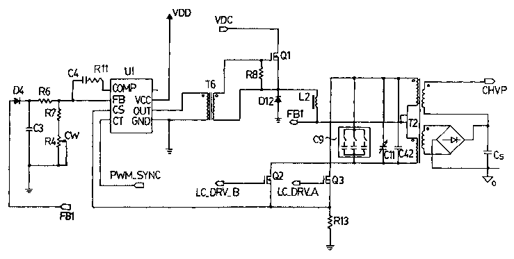
With reference to Figure 8, the resonant frequency of the column driving
resonant circuit is controlled by the effective inductance seen at the primary
of the
step-down transformer T2 and by the effective capacitance of the capacitor C42
in
parallel with the column capacitance as seen at the primary of T2. There is
also a
small trimming capacitor C11 in parallel with C42 for fine tuning of the
resonant
frequency. The turns ratio for the transformer is greater than 5 and the value
C, of
the capacitor C42, with reference to equation 2, is chosen so that C, is
substantially
greater than (n2/ n,) 2 CP to minimize the effect of changes in the panel
capacitance
on the resonant frequency. C9 is a bank of capacitors for tuning the tank
circuit, in
conjunction with the capacitance of C42, to obtain the desired resonant
frequency to
match or synchronize with different display scanning frequencies.
With further reference to Figure ~, the sinusoidal output at the secondary of
the transformer T2 is DC shifted by the voltage across the storage capacitor
CS of
the clamp circuit so that the instantaneous output voltage is never negative.
The resonant circuit is driven using the two MOSFETs Q2 and Q3, the
switching of which is controlled by the LC DRV signal that is synchronized
using an
appropriate delay time with the HSync signal thereby causing the row driver
ICs to
select the addressed row. The delay is adjusted to ensure that switching of
the row
driver ICs occurs when the drive current is close to zero. The LC DRV signal
is
generated by the low voltage logic section of the display driver that is
typically a field
programmable gate array (FPGA) but may be an application specific integrated
circuit (ASIC) designed for this purpose. The LC DRV signal is a 50% duty
cycle
CA 02471701 2004-06-25
WO 03/056538 PCT/CA02/02008
16
TTL level square wave. The LC DRV signal has two forms: the LC DRV A signal is
the complementary of the LC DRV B signal.
Again with respect to Figure 8, control of the voltage level in the resonant
circuit is achieved using the pulse width modulator U1 whose output is routed
through the transformer T6 to the gate of the MOSFET Q1. This controls the
voltage
level, in the resonant circuit by chopping the 330 volt input DC voltage. The
inductor
L2 limits the current to the resonant circuit as it is being energized from
the DC
voltage and the diode D12 limits voltage excursions at the source of the
MOSFET
Q1 due to current changes in the inductor. The duty cycle for the pulse width
modulator is controlled by a voltage feedback circuit for sensing the voltage
at the
primary of the transformer T2 to regulate or adjust the resonant circuit
voltage. The
switching of the pulse width modulator is synchronized with HSync using the
TTL
signal PWM SYNC from the low voltage logic section of the display driver.
With reference to Figure 9, the operation of the row driver circuit for the
preferred embodiment is similar to that of the column driver circuit, except
that the
turns ratio on the transformer T1 as compared to that of the transformer T2 in
the
column driver circuit is different to reflect the higher row voltages and
smaller values
of the panel capacitance as seen through the rows, due to the fact that the
remaining rows are at open circuit. There are also four more secondary
windings on .
the transformer T1 than there are on T2 to generate floating voltages required
for
operation of the polarity reversing circuit that alternates the polarity of
the rows on
successive frames.
In the preferred embodiment, the output of the row driver circuit feeds into
the
polarity reversing circuit shown in Figure 10. This provides row voltages
having
opposite polarity on alternate frames to provide the required ac operation of
the
electroluminescent display. Six MOSFETs Q4 through Q9 form a set of analogue
switches connecting either the positive or the negative sinusoidal drive
waveforms
generated to the panel rows. The selection of polarity is controlled by FRAME
POL,
a TTL signal generated by the system logic circuit in the display system. The
FRAME POL signal is synchronized to the vertical synchronization signal VSYNC
CA 02471701 2004-06-25
WO 03/056538 PCT/CA02/02008
17
that initiates scanning of each frame on the display. The FRAME POL signal,
together with four floating voltages from T1, generates the control signals
(FRAME_POL-1 to FRAME_POL-4) that operate the polarity reversing circuit.
Although alternate embodiments of the invention have been described herein,
it will be understood by those skilled in the art that variations may be made
thereto
without departing from the spirit of the invention or the scope of the
appended
claims.