Note: Descriptions are shown in the official language in which they were submitted.
CA 02471987 2007-06-04
1
DESCRIPTION
PLASMA SURFACE PROCESSING APPARATUS
Technical Field
This invention relates to a plasma surface processing technique, in
which a processing gas is plasmatized by impressing an electric field
between a pair of electrodes, processing such as film formation, etching,
ashing, cleaning, surface modification or the like is executed with respect
to the surface of a base material of a semiconductor base material or the
like. More particularly, the invention relates to an apparatus suited for
the so-called remote-control type in which a base material is arranged
away from an electric field impressing space between electrodes of a base
material, in a plasma film forming apparatus.
Background Art
The plasma surface processing apparatus is provided with a pair of
electrodes (for example, Japanese Patent Application Laid-Open No. H11-
236676). A processing gas is introduced between the pair of electrodes
and an electric field is also impressed there_between to generate a glow
discharge. By this, the processing gas is plasmatized. The processing
gas thus plasmatized is blown to the surface of a base material of a
semiconductor base material or the like. By this, such processing as film
formation (CVD), etching, ashing, cleaning and surface modification can
be conducted with respect to the surface of the base material.
The number of electrodes provided to a single apparatus is not
limited to two. For example, in a plasma processing apparatus disclosed
in Japanese Patent Application Laid-Open No. H05-226258, a plurality of
electrodes are arranged such that their polarities are alternately appeared.
A plasma surface processing system includes a so-called direct
CA 02471987 2004-06-25
2
system in which a base material is disposed in an electric field impressing
space between a pair of electrodes, and a so-called remote type in which a
base material is disposed away from an electric field impressing space and
a processing gas plasmatized in the electric field impressing space is
blown to this base material. It further includes a low pressure plasma
processing system in which the entire system is put into a pressure
reducing chamber and processing is conducted in a lower pressure
circumstance, and a normal pressure processing system in which
processing is conducted under pressure (generally normal pressure) close
to atmospheric pressure.
For example, as disclosed in Japanese Patent Application Laid-
Open No. H11-251304, the remote type normal pressure surface
processing apparatus comprises a blowoff nozzle for blowing out a
processing gas. Within this nozzle, a pair of electrodes are arranged in
opposing relation. At least one of the electrodes is provided at an
opposing surface thereof with a solid dielectric layer such as ceramic by
thermally sprayed coating film. This arrangement is made in order to
prevent the occurrence of arc discharge occurrable in a normal pressure
interelectrode space. The nozzle is formed with a blowoff passage which
is continuous with the electric field impressing space between the
electrodes. The base material is disposed ahead of this blowoff passage.
The gas to be used for plasma surface processing is selected
depending on the purpose of processing. In case of film formation
(CVD), gas containing the raw material of film is used. This raw
material gas is introduced between the electrodes and reacted with plasma
to form a film on the surface of a base material.
However, this film formation processing technique has such a
problem that the film, which is originally intended to be adhered to the
base material, is liable to adhere to the apparatus side. Particularly, in the
remote type, the gas is readily adhered to the surface of the electrode
CA 02471987 2004-06-25
3
before it is blown off from the blowoff passage. The gas is also readily
adhered to the peripheral area of the blowoff passage of the nozzle or to
the opposing surface of the nozzle with respect to the base material. This
results in loss of an increased amount of raw material. Maintenance such
as replacement of electrodes, etc. and cleaning thereof is more frequently
required. Total replacement of the main component such as electrodes
means significant waste of the component materials. Moreover, it is
extremely troublesome to totally clean the nozzle in order to remove the
adhesion (stain) adhered to the peripheral area of the blowoff passage. In
addition, the processing must be temporarily stopped during the
maintenance.
Incidentally, Japanese Patent Application Laid-Open No. H03-
248415 discloses a technique in which in the normal pressure CVD, in
general, the wall surface from the peripheral area of the nozzle to its
discharge part is composed of a wire netting and an inert gas is blown off
through the meshes of the wire netting, thereby to prevent the film from
adhering to the apparatus side. This techniques, however, again has such
a problem that the flow of processing gas is disturbed by the inert gas
coming through the meshes, thus badly degrading the film formation
efficiency onto the base material.
Moreover, the normal pressure plasma surface processing has such
a problem that an average free travel (life span) of the radicals is short
compared with the lower pressure circumstance. For this reason, if the
nozzle is arranged too away from the base material, it becomes unable to
form a film due to deactivation. On the other hand, if the nozzle is
arranged too close to the base material, arc is liable to occur between the
electrode on the side to which the electric field is impressed and the base
material, and the base material gets, in some instances, damaged.
In the normal pressure plasma surface processing, arc (abnormal
electric discharge) may occur at the rear surface (reversed side surface of
CA 02471987 2004-06-25
4
the opposing surface) of the electrode and at the edge of the electrode.
This occurs particularly significantly when rare gas including argon or
hydrogen is used as processing gas.
The present invention has been made in view of the above situation.
It is, therefore, an object of the present invention to provide a technique
for solving the problem of film adhesion to the electrodes, etc., at the time
of plasma film formation, particularly at the time of plasma film formation
according to the remote type, of all the plasma surface processing. It is
another object of the present invention to provide a technique capable of
conducting a favorable film formation processing while preventing the arc
discharge.
Disclosure of Invention
In order to solve the above-mentioned problems, according to a
first feature of the present invention, there is provided a plasma film
forming apparatus for forming a film on a surface of a base material under
the effect of plasma, comprising:
(A) a first gas supplying source containing a raw material of the film;
(B) a second gas supplying source caused by plasma discharge to reach
an excited state but containing no component capable of being formed into
the form of film; and
(C) a processing head which is to be placed opposite the base material;
the processing head being provided with:
(a) a grounded ground electrode; and
(b) an electric field impressing electrode connected to an electric
power source and forming a plasma discharge space between the ground
electrode and the electric field impressing electrode;
the processing head being formed with:
(c) a first flow passage for introducing a first gas from the first gas
supplying source to the base material in such a manner as to avoid or pass
CA 02471987 2004-06-25
very near the plasma discharge space; and
(d) a second flow passage including the plasma discharge space and
for causing a second gas coming from the second gas supplying source to
contact the first gas after allowing the second gas to pass through the
plasma discharge space.
Owing to the above arrangement, film can be prevented from
adhering to the surfaces of the electrodes which constitute the plasma
discharge space. Thus, loss of the raw material can be reduced.
Moreover, the trouble of maintenance such as replacement and cleaning of
the electrodes can be reduced.
In the first feature, it is accepted that, for example, the first and
second flow passages are converged with each other and continuous with a
common blowoff passage which is open to a surface of the processing
head which surface is to be placed opposite the base material (see FIG. 3,
as well as elsewhere). It is also accepted that downstream ends of the
first and second flow passages are spacedly open to a surface of the
processing head which surface is to be placed opposite the base material,
and the open ends serve as a blowoff port for the first gas and as a blowoff
port for the second gas, respectively (see FIG. 11, as well as elsewhere).
In the former common blowoff construction, the first gas and the
plasmatized second gas can be contacted in the common blowoff passage
so as to be reacted reliably. In the latter individual blowoff construction,
film can surely be prevented from being formed on the inner peripheral
surface of the blowoff passage.
In the common blowoff construction, for example, one of the first
and second flow passages is linearly continuous with the common blowoff
passage, and the other is crossed with the above-mentioned one flow
passage at an angle. One of the first and second gases can be linearly
flown in the blowoff direction and the other gas can be converged thereto.
The crossing angle between the first and second flow passages in
CA 02471987 2004-06-25
6
the common blowoff construction is, for example, right angle. However,
the crossing angle is not limited to this but it may be an obtuse angle or an
acute angle. Both the first and second flow passages may be angled with
respect to the common blowoff passage.
In the first feature, for example, the electrodes are provided as a
member for defining the first flow passage. Owing to this arrangement,
the specific first flow passage forming member can be omitted or made
short.
In the first feature, for example, the processing head is provided
with two electrodes which have the same polarities and which are
arranged in mutually adjacent relation, and the first flow passage is formed
between the electrodes having the same polarities. The electrodes having
the same polarities may refer to the electric field impressing electrodes, or
they may be the ground electrodes.
In the first feature, for example, the processing head is provided
with two each of the electric field impressing electrodes and ground
electrodes, thus four in total, the two electric field impressing electrodes
are arranged in mutually adjacent relation thus forming the first flow
passage therebetween, and the two each electric field impressing
electrodes are placed opposite the two each corresponding ground
electrodes thus forming the plasma discharge space therebetween (see FIG.
3, as well as elsewhere).
The four electrodes are arranged, for example, in the order of the
ground electrode, the electric field impressing electrode, the electric field
impressing electrode and the ground electrode, and owing to this
arrangement, the two plasma discharge spaces and thus the second flow
passages are arranged on both sides with the single first flow passage
sandwiched therebetween.
In this four-electrode and three-flow passage construction, for
example, the processing head includes a base material opposing member
CA 02471987 2004-06-25
7
which is to cover a surface to be faced with the base material of the
electrode, and the base material opposing member formed with respective
blowoff passages of the three flow passages (see FIG. 11). Owing to this
arrangement, one mode of the individual blowoff construction is
constituted.
Moreover, in the four-electrode and three-flow passage
construction, it is accepted that the processing head includes a base
material opposing member which is to cover a surface to be faced with the
base material of the electrode, a communication passage is formed as a
part of the second flow passage between the base material opposing
member and each electric field impressing electrode, the plasma discharge
space and the first flow passage is communicated with each other through
the communication passage, and the base material opposing member is
formed with a common blowoff passage of the first and second gases such
that the common blowoff passage is continuous with a crossing part
between the first flow passage and the communication passage (see FIG.
3). Owing to this arrangement, one mode of the individual blowoff
construction is constituted.
The base material opposing member is composed, for example, of
an insulative (dielectric) material such as ceramic.
As a more generalized construction of the four-electrode and three
flow passage construction, it is accepted that the processing head is
provided with a plurality of electric field impressing electrodes and a
plurality of ground electrodes, and the electrodes are arranged in parallel
relation such that first flow passages each formed between the electrodes
having the same polarities and plasma discharge spaces, i.e., second flow
passages each formed between the electrodes having different polarity are
alternately arranged (see FIG. 13). The terms "electrodes having the
same polarities refer to the electric field impressing electrodes or refer to
ground electrodes, and the terms "electrodes having different polarities"
CA 02471987 2004-06-25
g
refer to the electric field impressing electrode and the ground electrode.
In this first and second flow passages alternately arranged
construction, it is preferable that the electrodes located at opposite end
parts in the arrangement direction are ground electrodes. Owing to this
arrangement, electric field can be prevented from leaking outside of the
row of electrodes.
In the alternately arranged construction, the first and second flow
passages may be arranged alternately one by one, or one group by one
group. The first group consists of the first flow passage(s) and the second
group consists of the second flow passage(s). The second flow passages
and the first flow passages may be arranged alternately such that only one
first flow passage is arranged after a plurality of second flow passages.
In the alternative, they may be arranged alternately such that a plurality of
first flow passages are arranged after only one second flow passage. One
group of the first or second flow passages may be different in number in
accordance with the arranging direction. Preferably, the number of the
second flow passages is larger, as a whole, than that of the first flow
passages. Owing to this arrangement, sufficient reaction of the raw
material gas can be obtained.
In the first feature, for example, the electric field impressing
electrode and the ground electrode extend in a direction orthogonal to the
opposing direction of the electric field impressing electrode and the
ground electrode, an upstream end of the plasma discharge space between
the electrodes is disposed at one end part in a first direction orthogonal to
the opposing direction and extending direction, and a downstream end
thereof is disposed at the other end part in the first direction. Owing to
this arrangement, the range can be enlarged in which a film can be formed
at a time and the processing efficiency can be enhanced.
In the elongate electrode construction, it is preferable that an
electricity feed line to the electric field impressing means is connected to
CA 02471987 2004-06-25
9
one end part in the longitudinal direction of the electric field impressing
electrode, and a ground line is connected to the other end part in the
longitudinal direction of the ground electrode (see FIG. 6). Owing to this
arrangement, the electricity feed line and the ground line can be prevented
from being short-circuited.
In one preferred mode of the first feature, the ground electrode is
arranged in opposing relation on the side of the electric field impressing
electrode which is to be faced with the base material in the processing
head (see FIG. 15). Owing to this arrangement, arc can be prevented
from occurring between the electric field impressing electrode and the
base material by interposing the ground electrode between the electric
field impressing electrode and the base material. Thus, the base material
can be prevented from being damaged, and the processing head and thus,
the plasma discharge space can be located sufficiently close to the base
material. As a result, the active pieces can surely be brought to the base
material before the active pieces lose activity, and a high-speed and
favorable film forming processing can be conducted. This interposing
construction is particularly effective for the generally normal pressure
plasma film formation processing in which an average free travel of
radicals (distance until the active pieces lose activity) is short.
The terms "generally normal pressure (close to atmospheric
pressure)" used herein refers to a range from 1.333 x 10⁴ to 10.664 x 1W
Pa. Particularly, a range from 9.331 x 10⁴ to 10.397 x 10' Pa is
preferable because pressure adjustment becomes easy and the construction
of the apparatus becomes simplified.
In the ground electrode interposing construction, for example, the
processing head includes a base material opposing member which is to
cover a surface to be faced with the base material of the electric field
impressing electrode, and the ground electrode is disposed at the base
material opposing member. A gap is formed between the electric field
CA 02471987 2004-06-25
impressing electrode and the base material opposing member, and the gap
serves as a second flow passage including the plasma discharge space. It
is preferable that the plasma discharge space is directly crossed with the
first flow passage, and the base material opposing member is formed with
a common blowoff passage of the first and second gases such that the
common blowoff passage is continuous with the crossing part.
According to this directly converging construction, the plasma in the
discharge space can be overflowed to the crossing part. By this
overflowed part, the first gas can directly be plasmatized (the first gas can
pass very near the plasma discharge space). Owing to this arrangement,
the film forming efficiency can be enhanced.
In the ground electrode interposing construction, for example, the
receiving recess for receiving the ground electrode is formed in a surface
(surface on the reversed side of the electric field impressing side) to be
faced with the base material of the base material opposing member.
Owing to this arrangement, the ground electrode is directly faced with the
base material. In this ground electrode directly opposing construction, it
is preferable that the base material opposing member is composed of
ceramic, and a forming part for forming the receiving recess of the base
material opposing member is provided as a solid dielectric layer which is
to cover a metal main body of the ground electrode. Owing to this
arrangement, it is no more required to provide a specific solid dielectric
layer to the ground electrode.
In the ground electrode interposing construction, for example, an
end face to be faced with the common blowoff passage of a metal main
body of the electric field impressing electrode may be generally flush with
(see FIG. 20) or more expanded than an end face on the same side of the
metal main body of the electric field impressing electrode. It is also
accepted that an end face on the side facing with the common blowoff
passage of the metal main body of the ground electrode is more retracted
CA 02471987 2004-06-25
11
than an end face on the same side of the metal main body of the electric
field impressing electrode (see FIG. 21). In the former generally flush or
expanded construction, the electric field can surely be prevented from
leaking to the base material side from the ground electrode, arc can surely
be prevented from falling onto the base material, and the distance between
the processing head and the base material can surely be reduced. In the
latter retracted construction, a lateral electric field can be formed between
the end faces of the electric field impressing electrode and the ground
electrode, and the reaction space for the first gas can be located closer to
the base material.
In the first feature, for example, the processing head is provided
with a grounded conductive member such that the grounded conductive
member covers a side to be faced with the base material of the electric
field impressing electrode (FIGS. 15 and 23, as well as elsewhere).
Owing to this arrangement, arc can be prevented from occurring between
the electric field impressing electrode and the base material by interposing
the grounded conductive member between the electric field impressing
electrode and the base material. Thus, the base material can be prevented
from being damaged, and the processing head and thus, the plasma
discharge space can be located sufficiently close to the base material. As
a result, the active pieces can surely be brought to the base material before
the active pieces lose activity, and a high-speed and favorable film
forming processing can be conducted. This interposing construction is
particularly effective for the generally normal pressure plasma film
formation processing in which the average free travel of the radicals
(distance until the active pieces lose activity) is short.
In this conductive member interposing construction, it is accepted
that the conductive member forms a plasma discharge space between the
electric field impressing electrode and the conductive member, and the
conductive member is provided as the ground electrode (see FIG. 15).
CA 02471987 2004-06-25
12
Owing to this arrangement, the conductive member can also serve as the
ground electrode and thus, the number of parts can be reduced.
In the conductive member interposing construction, an insulative
member for insulating the conductive member and the electric field
impressing electrode may be filled between the insulative member and the
electric field impressing electrode (see FIG. 23). Owing to this
arrangement, electric discharge can be prevented from occurring between
the conductive member and the electric field impressing electrode.
In the first feature, it is preferable that the processing head is
provided with an intake duct having an intake port surrounding a
peripheral edge part of a base material opposing surface thereof. Owing
to this arrangement, the processed gas can be prevented from remaining in
the space and discharged smoothly. Eventually, stain adhered to the base
material opposing member can be reduced, and the frequency of
maintenance can be reduced. Moreover, the flow of the first and second
gases can be stabilized in the space between the processing head and the
base material, and a generally laminar flow state can be attained.
According to a second feature of the present invention, there is
provided a plasma film forming apparatus for forming a film on a surface
of a base material under the effect of plasma, comprising:
a first gas supplying source containing a raw material of the film;
a second gas supplying source caused by plasma discharge to reach
an excited state but containing no component for capable of being formed
into the form of film;
a grounded ground electrode;
an electric field impressing electrode connected to an electric
power source and forming a plasma discharge space in such a manner as to
oppose the ground electrode;
a first flow passage forming means for flowing therethrough a first
gas from the first gas supplying source in such a manner as to avoid or
CA 02471987 2004-06-25
13
pass very near the plasma discharge space and blowing the first gas to the
base material; and
a second flow passage forming means for allowing a second gas
coming from the second gas to pass through the plasma discharge space
and causing the second gas to contact the first gas. Owing to this
arrangement, film can be prevented from adhering to the surfaces of the
electrodes which constitute the plasma discharge space. Thus, the raw
material loss can be reduced. Moreover, the trouble of maintenance such
as replacement of the electrodes and cleaning thereof can be reduced.
As mentioned above, the electrodes having the same polarities can
be the first flow passage forming means, and the electrodes having
different polarities can be the second flow passage forming means. That
is, it is accepted, for example, that the electric field impressing electrode
includes a surface forming a first flow passage and provided as the first
flow passage forming means. Moreover, it is also accepted that the
electric field impressing electrode and the ground electrode are provided
as the second flow passage forming means, in which a second flow
passage and thus, a plasma discharge space are formed between the
electric field impressing electrode and the ground electrode.
According to another mode of the second feature, the ground
electrode is arranged on the side to be faced with the base member of the
electric field impressing electrode with a dielectric member (insulative
member) sandwiched between the ground electrode and the electric field
impressing electrode, and a cutout for allowing the dielectric member to
be exposed therethrough is formed in a part of the ground electrode, the
inside of the cutout serves as the plasma discharge space; the second flow
passage forming means makes the second gas blow out along the ground
electrode and enter the cutout; and the first flow passage forming means
makes the first gas blow out on the reverse side to the ground electrode
from the second gas in such a manner as to form a laminar flow with the
CA 02471987 2004-06-25
14
second gas (see FIG. 22). Owing to this arrangement, the first gas can be
flown in such a manner as to pass very near the plasma discharge space
and reacted nearer to the base material. Moreover, the film adhesion to
the apparatus side can be restrained.
In a plasma surface processing (particularly normal pressure
surface processing) as in the present invention, a solid dielectric layer for
preventing the occurrence of arc (abnormal electric discharge) is provided
to at least one of the opposing surfaces of the electric field impressing
electrode and the ground electrode. This solid dielectric layer may be
coated on the metal main body of the electrode by thermally sprayed
coating or the like (see FIG. 3). In the alternative, it may be of a
dielectric case receiving structure as described hereinafter.
That is, the electrode of the plasma film forming apparatus of the
present invention may comprise a main body composed of metal, and a
dielectric case composed of a solid dielectric member for receiving therein
the main body (FIG. 19). Owing to this arrangement, even if a film
(stain) should be adhered to the electrode, it would be adhered only to the
dielectric case and would not be adhered to the electrode main body.
Therefore, simply by cleaning only the dielectric case, the main body can
be used as it is. Moreover, since the entire electrode main body is
covered with the dielectric case as the solid dielectric layer, abnormal
electric discharge can be prevented from occurring not only at the
opposing surface with respect to the other electrode but also at the rear
surface and the edge. Particularly, even in case such substance easy to
discharge as argon or hydrogen is used as the processing gas, abnormal
electric discharge can surely be prevented from occurring at the rear
surface, etc. Moreover, it is easy to apply variation to the thickness
compared with the technique in which the surface of the electrode main
body is directly coated by thermally sprayed coating or the like. The
dielectric case receiving construction itself can be applied not only to the
CA 02471987 2004-06-25
plasma film formation which belongs to the field of the present invention
but also widely to other plasma surface processing electrode construction
such as cleaning, etching, ashing, surface modification and the like. It
can be applied not only to the remote type plasma processing but also to
direct type.
Preferably, the dielectric case includes a case main body
retractably receiving the electric main body in an internal space whose one
surface is open, and a lid for covering the opening.
Both the paired electric field impressing electrode and the ground
electrode may be of the dielectric case receiving construction. In that
case, the plasma discharge space of the second flow passage is formed
between the dielectric case of the electric field impressing electrode and
the dielectric case of the ground electrode.
It is accepted that each of the two electrodes having same polarities
and forming the first flow passage comprise a main body composed of
metal and a dielectric case composed of a solid dielectric member for
receiving therein the main body, the dielectric cases of the electrodes are
placed opposite each other, thereby forming the first flow passage
therebetween.
The dielectric cases of the electrodes may be separately formed, or
they may be integrally connected to one another (see FIG. 28, as well as
elsewhere). In the former separate construction, maintenance such as
replacement can be conducted individually depending on the status of
adhesion (stain). In the latter integral construction, the number of parts
can be reduced. In addition, relative positioning and the like of the
electrodes can be conducted easily and correctly. In case of the integral
construction, it is preferable that a gas flow passage is formed in the case
main body, and receiving spaces for receiving the electrode main body
therein are formed on both sides with this flow passage sandwiched
therebetween. It is accepted that the sectional area of this flow passage is
CA 02471987 2004-06-25
16
varied along the gas flowing direction such that the passage becomes
gradually narrow or wide, or it is provided with a step. Owing to this
arrangement, the pressure and speed of the gas flow can be changed.
According to the integral construction, such a deformed flow passage as
just mentioned can be formed easily.
It is accepted that each electrode and thus the dielectric case
thereof extend in a direction orthogonal to the opposing direction with
respect to the other electrode, and the dielectric case integrally includes a
gas uniformizing part for uniformly dispersing gas, which is introduced
into a flow passage between the dielectric case and the other electrode, in
the extending direction (see FIG. 30). Owing to this arrangement, an
additional member of uniformizing gas is not more required, and the
number of parts can be reduced.
The thickness of a plate part on the side forming the plasma
discharge space in the dielectric case may be different between the
upstream side and the downstream side of the plasma discharge space (see
FIG. 28). Moreover, in the case integral construction, it is accepted that
the integral dielectric case is formed with a second flow passage serving as
the plasma discharge space, a metal main body is received in each side of
the integral dielectric case with the flow passage sandwiched therebetween,
and a distance between the metal main bodies is different between the
upstream side and the downstream side of the plasma discharge space (see
FIG. 29). Owing to this arrangement, many variations can be applied to
the status of plasma by varying the manner for generating the radical
species as it flows. Thus, the surface processing recipe can be enriched.
It is accepted that each electrode comprises a metal-made main
body and a solid dielectric layer disposed at least at the plasma discharge
space forming surface of the main body, and the thickness of the solid
dielectric layer at the plasma discharge space forming surface is different
between the upstream side and the downstream side of the plasma
CA 02471987 2004-06-25
17
discharge space. It is also accepted that each electrode comprises a
metal-made main body and a solid dielectric layer disposed at least at the
plasma discharge space forming surface of the main body, and a distance
between the two electrodes is different between the upstream side and the
downstream side of the plasma discharge space.
As means for impressing electric field to the electrodes or as
grounding means of the present invention, a feed or grounding pin may be
used, or a covered conductor may be connected directly to the electrode.
In the former pin construction, the pin includes a conductive pin
main body having a pin hole opening to a tip end face thereof and
withdrawably embedded in the electrode, a core member electrically
connected with the pin main body and slideably received in the pin hole,
and a spring received in the pin hole and for biasing the core member so as
to be pushed out of the tip end opening of the pin hole (see FIG. 10).
Owing to this arrangement, the pin and the electrode can surely be
electrically conducted. Moreover, since the power feed pin can be
withdrawn from the electrode, it cannot be any interference at the time of
maintenance.
In the latter covered conductor construction, it is preferable that a
conductor hole is formed in the electrode, the covered conductor is
inserted in the conductor hole, the covered conductor is formed by
covering a conducting wire with an insulative material, only a tip part of
the wire located on an inner side of the hole is exposed from the insulative
material, a screw is screwed in the electrode in such a manner as to be
generally orthogonal to the conductor hole, and the screw presses the
exposed tip part of the wire against an inner peripheral surface of the
conductor hole (FIG. 24). Owing to this arrangement, the conductive tip
part can surely be fixed to the electrode main body. Moreover, abnormal
electric discharge can surely be prevented from occurring at the pulled-out
part of the conductor from the electrode. At the time of maintenance, the
CA 02471987 2004-06-25
18
conductor can easily be withdrawn from the electrode by loosening the
screw.
In the first feature, it is preferable that the processing head
removably includes a base material opposing member formed with a first
and a second gas blowoff passage and disposed opposite the base material
(see FIG. 9). Owing to this arrangement, even if a film (stain) should be
adhered to the base material opposing surface of the processing head, etc.,
only the base material opposing member can be separated. Then, only
the base material opposing member can be cleaned by being dipped into a
chemical liquid such as, for example, strong acid. Therefore, it is no
more required to bring the entire processing head to the cleaning process,
and the maintenance can be simplified. Moreover, by preparing a spare
part of the base material opposing member, the surface processing can be
kept continued even during the time of maintenance.
The removing construction itself of the base material opposing
member can be applied not only to the plasma film formation which
belongs to the field of the present invention but also widely to other
plasma surface processing head such as cleaning, etching, ashing, surface
modification and the like. Moreover, it can also be applied to other
surface processing heads than plasma such as thermal CVD.
In the opposing member removing construction, it is preferable to
further comprise support means for supporting the base material opposing
member in such a manner as to place a peripheral edge part of the base
material opposing member thereon with a surface to be faced with the base
material of the base material opposing member directing downward; an
upper side part from the base material opposing member of the processing
head being integrally placed on the base material opposing member.
Moreover, it is preferable that the support means has a frame-like
configuration so that the processing head can be receiving therein in such
manner as to be able to be removed upward, and an inner flange for
CA 02471987 2004-06-25
19
hooking on a peripheral edge part of the base material opposing member is
disposed at an inner peripheral edge of a lower end part of the support
means. Owing to this arrangement, simply by pulling up the processing
head, the base material opposing member can be separated at the time of
maintenance. Moreover, a processing head directing downward is
constituted and the base material is disposed beneath the head.
In the opposing member removing construction, it is preferable
that a positioning protrusion is disposed at one of the upper side part from
the base material opposing member of the processing head and the support
means, and a positioning recess for allowing the positioning protrusion to
be vertically fitted thereto is disposed at the other of the upper side part
from the base material opposing member of the processing head and the
support means. Owing to this arrangement, the processing head can
surely be positioned at the support means.
The support means preferably includes an intake duct having an
intake port which is open downward and disposed in such a manner as to
surround the processing head. Owing to this arrangement, the processed
gas can be prevented from remaining in the space and discharged
smoothly. Eventually, stain adhered to the base material opposing
member can be reduced, and the frequency of maintenance can be reduced.
Moreover, since the support means and the intake duct are composed of a
common member, the number of parts can be reduced.
In the first feature, it is preferable that the processing head includes
a member to be faced with the base material, the base material opposing
member includes a blowoff region where the first and second gas blowoff
passages are disposed and an expanding region expanded from the blowoff
region thereby to gain a ratio for forming a film, and the expanding region
is connected with an inert gas introduction means; and the expanding
region of the base material opposing member is composed of a material
having such a degree of gas permeability that the inert gas coming from
CA 02471987 2004-06-25
the gas introduction means is allowed to permeate toward a base material
opposing surface and the degree of permeation and thus the degree of
oozing of the inert gas from the base material opposing surface is such that
the processing gas can be prevented from contacting the base material
opposing surface without disturbing a flow of the processing gas (see FIG.
34). Owing to this arrangement, a thin layer of inert gas can be formed
on the base material opposing surface, particularly on the expanding
region, so that film can surely be prevented from adhering to the base
material opposing surface. In addition, a film can sufficiently be formed
while guiding the processing gas to the expanding region without
disturbing the processing gas flow in the space between the processing
head and the base material.
The gas permeating material is preferably a porous material.
Owing to this arrangement, the desired degree of permeation and thus
oozing-out can be obtained easily and reliably. Particularly, by
composing the gas permeating material from a porous material, an
insulative property can surely be obtained, too.
It is preferable that a groove for temporarily storing therein the
inert gas coming from the gas introduction means is formed in an opposite
side surface to the base material opposing surface in the expanding region
of the base material opposing member in such a manner as to be recessed
toward the base material opposing surface. Owing to this arrangement,
the base material opposing member in the expanding region can be
reduced in thickness, and an inert gas film can surely be formed on the
base material opposing surface, thereby a film can be prevented from
being adhered to this surface more reliably.
It is preferable that the base material opposing member has a short
direction and a longitudinal direction, each of the regions extends in the
longitudinal direction, the expanding region is provided at both sides in
the short direction with the blowoff region sandwiched therebetween, and
------ ------
CA 02471987 2004-06-25
21
the groove is formed in each expanding direction in such a manner as to
extend in the longitudinal direction. Owing to this arrangement, a film
can efficiently be formed over a wide range of area at a time, and a film
can surely be prevented from adhering to the two expanding regions.
It is preferable that the base material opposing member is entirely
integrally formed from a gas permeating material, and a gas permeation
prohibiting member for prohibiting gas permeation is disposed at an inner
side surface facing with the blowoff region of the groove. Owing to this
arrangement, the processing gas flow can surely be prevented from being
disturbed or diluted in the blowoff region by inert gas, and therefore, a
high quality film formation can be enjoyed.
It is preferable that the groove is provided at an intermediate part
thereof in a direction of the depth with a partition, the partition has a
sufficiently higher gas permeability than the gas permeating material, and
the groove is partitioned into an upper-stage groove part continuous with
the inert gas introduction means and a lower-stage groove part near the
base material opposing surface through the partition. Owing to this
arrangement, the inert gas can be uniformized within the groove. The
partition is preferably composed of a porous plate which is more rough
enough in mesh than the gas permeating material. Moreover, the gas
permeation prohibiting member is preferably disposed only at the inner
side surface directing the blowoff region of the upper-stage groove part.
The lower-stage groove part is preferably larger in capacity than the
upper-stage groove part. By disposing the gas permeation prohibiting
member only at the upper-stage groove part, the lower-stage groove can be
made larger in capacity than the upper-stage groove part.
In the first feature, it is preferable that a downstream end of the
first flow passage is crossed with a downstream end of the second flow
passage, and the crossing part serves as a common blowoff port of the first
and second gases (see FIG. 37). Owing to this arrangement, a film can
CA 02471987 2004-06-25
22
be prevented from adhering to the opposing surfaces of the respective
electrodes. Moreover, the first gas and the plasmatized second gas can
be mixed with each other simultaneously with the blowoff, and a sufficient
film forming reaction can be obtained without waiting for dispersion of
the gases and before the active species are not lost in activity. Thus, the
film forming efficiency can be enhanced.
In this mixing simultaneous blowoff construction, the first and
second flow passages are preferably crossed with each other at an acute
angle. Owing to this arrangement, the first and second gases can be
blown against the base material while being mixed such that the first and
second gases form a single flow.
In the mixing simultaneous blowoff construction, it is preferable
that the processing head includes a surface where the blowoff port is open
and which is to be faced with the base material, one of the first and second
flow passages is orthogonal to the base material opposing surface, and the
other is slantwise to the base material opposing surface and crossed with
the one flow passage at an acute angle. Owing to this arrangement, by
blowing off one of the gases against the base material from right in front
thereof and diagonally converging the other gas to the first-mentioned gas,
a single gas flow can be obtained.
In the mixing simultaneous blowoff construction, it is preferable
that the first and second flow passages are arranged such that the second
flow passage is disposed in such a manner as to sandwich or surround the
first flow passage with the second flow passage disposed therebetween,
and the second flow passage is approached to the first flow passage toward
the downstream end and crossed with each other at the blowoff port.
Owing to this arrangement, the second gas can be converged to the
opposite sides or around the first gas. One example, in which "the
second flow passages sandwich the first flow passage therebetween"
includes an arrangement in which two second flow passages are arranged
CA 02471987 2004-06-25
23
on the opposite sides of the first flow passage. Similarly, one example, in
which "the second flow passages surround the first flow passage" includes
an arrangement in which the second flow passages are concentrically
arranged with the first flow passage disposed therebetween, so that the
second flow passages will approach the first flow passage. The
concentric second flow passages may have an annular configuration in
section enabling to surround the first flow passage, and are gradually
reduced in diameter toward the downstream. In the alternative, the
concentric second flow passages may be constructed such that they are
composed of a plurality of branch passages spacedly arranged in the
peripheral direction of the first flow passage in such a manner as to
surround the first flow passage, and those branch passages gradually
approach the first flow passage toward the downstream. The first and
second flow passages may be in reversed relation. That is, it is also
accepted that the first flow passages are arranged such that they sandwich
or surround the second flow passage disposed therebetween, and the first
flow passages gradually approach the second flow passage toward the
downstream side and finally crossed with each other at the blowoff port.
In the mixing simultaneous blowoff construction, it is preferable
that the processing head is provided with two each of the electric field
impressing electrodes and the ground electrodes, the two electric field
impressing electrodes are disposed at the first flow passage in such a
manner as to be faced with each other, one each of the electric field
impressing electrodes is faced with one each of the ground electrodes with
the second flow passage formed therebetween, the two second flow
passages are arranged in such a manner as to be approached to the first
flow passage toward the downstream end with one of the first flow
passages sandwiched therebetween, and three of those passages are
crossed with one another at the blowoff port. Owing to this arrangement,
the plasmatized second gas can be converged to the first gas from both
CA 02471987 2004-06-25
24
side of the first gas.
Moreover, it is preferable that the processing head includes a
surface where the blowoff port is open and which is to be faced with the
base material; the first flow passage between the two electric field
impressing electrodes is orthogonal to the base material opposing surface,
each of the two electric field impressing electrodes includes a first surface
located on the reverse side to the side which is faced with the first flow
passage and slantwise with respect to the base material opposing surface;
and each of the two ground electrodes includes a second surface which is
faced in parallel with the first surface of the corresponding electric field
impressing electrode and forming the second flow passage therebetween.
Owing to this arrangement, the respective electric field impressing
electrodes can be arranged on the reverse side to the base material with the
ground electrode sandwiched therebetween, arc discharge to the base
material from the electric field impressing electrodes can be prevented
from occurring, and a favorable film forming processing can surely be
conducted. Moreover, by blowing off the first gas against the base
material from right in front thereof and diagonally converging the
plasmatized second gas to the opposite sides of the first gas, a single gas
flow can be obtained.
In the construction having two second flow passages arranged on
opposite sides of the first flow passage, the two second flow passages are
preferably symmetrical with each other with the first flow passage
sandwiched therebetween. Owing to this arrangement, the plasmatized
second gas can be uniformly converged to the first gas from the opposite
sides of the first gas.
The ground electrode preferably includes the base material
opposing surface. Owing to this arrangement, arc discharge to the base
material from the respective electric field impressing electrodes can more
surely be prevented from occurring.
CA 02471987 2004-06-25
Brief Description of Drawings FIG. 1 is a schematic view of a plasma film
forming apparatus
according to a first embodiment of the present invention.
FIG. 2 is a front sectional view of a gas uniformizing part of a
processing head of the plasma film forming apparatus.
FIG. 3 is a front sectional view of a nozzle part of the processing
head.
FIG. 4 is a side sectional view taken along the longitudinal
direction of the gas uniformizing part.
FIG. 5 is a side sectional view of the nozzle part taken on line V-V
of FIG. 3.
FIG. 6 is a plan sectional view of a left side part of the nozzle part
taken on line VI-VI of FIG. 3.
FIG. 7 is a bottom view of the processing head.
FIG. 8 is an enlarged view of a gas blowoff part of the processing
head.
FIG. 9 is a front sectional view showing a manner for separating a
head main body of the processing head and a nozzle tip composing
member at the time of maintenance.
FIG. 10 is a detailed view of a power feed pin of the nozzle part.
FIG. Il is a front sectional view of a nozzle part of a processing
nozzle in a plasma film forming apparatus according to a second
embodiment of the present invention.
FIG. 12 is a bottom view of the processing head of the second
embodiment.
FIG. 13 is a front sectional view of a processing head in a plasma
film forming apparatus according to a third embodiment of the present
invention.
FIG. 14 is a sectional view showing a modified embodiment of the
CA 02471987 2004-06-25
26
third embodiment.
FIG. 15 is a front sectional view of a nozzle part of a processing
head in a plasma film forming apparatus according to a fourth
embodiment of the present invention.
FIG. 16 is a side sectional view of the nozzle part taken on line
XVI-XVI of FIG. 15.
FIG. 17 is a plan sectional view of the nozzle part taken on line
XVII-XVII of FIG. 15.
FIG. 18 is a bottom part of a processing head of the fourth
embodiment.
FIG. 19 is an exploded perspective view of an electric field
impressing electrode of the fourth embodiment.
FIG. 20 is an enlarged view of a gas blowoff part of the fourth
embodiment.
FIG. 21 is an enlarged view of a gas blowoff part showing a
modified embodiment of a ground electrode structure of the fourth
embodiment.
FIG. 22 is a schematic construction view of a plasma film forming
apparatus according to a fifth embodiment of the present invention.
FIG. 23 is a schematic structure view of a plasma film forming
apparatus according to a sixth embodiment of the present invention.
FIG. 24 is a sectional view showing a modified embodiment of a
connection structure of an electric field impressing electrode and an
electricity feed line.
FIG. 25 is an exploded perspective view showing a modified
embodiment of an induction case of an electrode.
FIG. 26 is a front sectional view showing another modified
embodiment of an induction case.
FIG. 27 is an exploded perspective view of the induction case of
FIG. 26.
CA 02471987 2004-06-25
27
FIG. 28 is a perspective view showing a modified embodiment of
an electrode structure with an induction case.
FIG. 29 is a perspective view showing another modified
embodiment of an electrode structure of an induction case.
FIG. 30 is a front sectional view of an electrode structure having a
gas uniformizing part integrated induction case.
FIG. 31 is a side view of a gas uniformizing part integrated
induction case taken on line XXXI-XXXI of FIG. 30.
FIG. 32 is a front sectional view of an electrode structure having
an induction case with a tree-type passage.
FIG. 33 is a side view of the induction case with a tree-type
passage taken on line XXXIII-XXXIII of FIG. 32.
FIG. 34 is a view showing a schematic construction of a normal
pressure plasma film forming apparatus according to a seventh
embodiment of the present invention and a front section of a processing
head of the apparatus.
FIG. 35 is a plan view of a lower plate of the processing head
taken on line XXXV-XXXV of FIG. 34.
FIG. 36 is a side sectional view of a nozzle part of the processing
head taken on line XXXVI-XXXVI of FIG. 35.
FIG. 37 is a view a schematic construction of a normal pressure
plasma film forming apparatus according to an eighth embodiment of the
present invention and a front section of a processing head of the apparatus.
FIG. 38 is an enlarged sectional view of a nozzle of the processing
head of FIG. 37.
Best Mode for Carrying Out the Invention
Embodiments of the present invention will be described hereinafter
with reference to the drawings.
FIG. 1 shows a normal pressure plasma film forming apparatus M l
CA 02471987 2004-06-25
28
according to a first embodiment of the present invention. The normal
pressure plasma film forming apparatus M1 comprises a frame (support
means) including a housing 10, a processing head 3 supported on the
housing 10 of the frame, two kinds of processing gas sources 1, 2
connected to the processing head 3, and a power source 4. Beneath the
processing head 3, a plate-like base material W (material to be processed)
having a large area is transferred in the left and right direction by transfer
means (not shown) It is, of course, accepted that the base material W is
fixed and the processing head 3 is moved. In the normal pressure plasma
film forming apparatus Ml, a film A (FIG. 8) such as, for example,
amorphous silicon (a-Si) and silicon nitride is formed on an upper surface
of this base material W.
Of the two kinds of processing gas sources, a raw material gas
source 1(first gas source) stores therein a raw material gas (first gas, for
example, silane) which forms a film A such as the above-mentioned
amorphous silicon. An excitable gas source 2 (second gas source) stores
therein an excitable gas (second gas, for example, hydrogen and nitrogen).
The excitable gas, when excited by plasma, causes the raw material such
as the silane to be reacted to form the film A such as amorphous silicon or
the like. On the other hand, the excitable gas does not include a
component (film raw material) which is not formed into a film alone even
when excited by plasma. Each gas may be stored in a liquid phase and
evaporated by an evaporator.
The raw material gas and the excitable gas is generally referred to
as the "processing gas".
A pulse power source 4 (electric field impressing means) outputs a
pulse voltage to the electrode 51. This pulse voltage preferably has a
pulse rise time and/or pulse fall time of 10 g s or less, 200 g s or less of
pulse duration, 1 to 1000 kV/cm of electric field strength, and 0.5 kHz or
more of frequency.
CA 02471987 2004-06-25
29
The housing 10 for receiving and supporting the processing head 3
includes a left and a right wall l l having, for example, a semi-circular
configuration in side view and a front and a rear low wall for connecting
the lower parts of the walls 11. The housing 10 has a square
configuration in plane view. The housing 10 as a support means of the
processing head 3 also serves as an intake duct. That is, as shown in
FIGS. 3 and 6, the front, rear, left and right walls 11, 12 are of hollow
structure. The lower end parts of those hollow parts 10b are open to the
lower end faces of the walls 11, 12, thereby forming an intake port l0a
surrounding the outer periphery of the lower end of the processing head 3.
As shown in FIG. 1, openings llb continuous with the hollow parts lOb
are disposed at the upper end parts of the left and right walls 11. A gas
exhaust passage 13 extends from each upper end opening l lb. After
converged, those gas exhaust passages 13 are connected to a pump 14 (gas
exhaust means).
The processing head 3 has a generally rectangular parallelepiped
configuration which is long is the back and forth direction. The
processing head 3 is received in and supported by the housing 10 such that
the processing head 3 is surrounded with the front, rear, left and right
walls 11, 12. The support structure of the processing head 3 will now be
described.
As shown in FIGS. 3 and 7, the housing 10 is provided at the lower
end edges of the inner wall surfaces of the left and right walls 11 each with
an inner flange l ld. A lower frame 24 of the processing head 3 is placed
on the inner flanges 11d such that the left and right parts of the lower
frame 24 are hooked on the inner flanges lld. As shown in FIGS. 5 and
7, the housing 10 is also provided at the front and rear walls 12 each with
an inner flange 12d. The front and rear parts of the lower frame 24 are
placed on the inner flanges 12d, respectively.
As shown in FIG. 1, the front and rear walls 12 are formed at the
CA 02471987 2004-06-25
upper end faces each with a positioning recess 12b (head support part)
which is recessed in a form of a reversed triangle. On the other hand, a
side frame 23 of the processing head 3 is provided with a positioning
protrusion 23a which has a reversed triangular configuration. The
positioning protrusion 23a is fitted to the positioning recess 12b. Owing
to this arrangement, the processing head 3 is positioned to and supported
by the housing 10.
It is also accepted that the positioning recess is provided at the
processing head 3 and the positioning protrusion is provided at the
housing (support means) 10.
As shown in FIG. 1, the processing head 3 is comprised of a gas
uniformizing part 30 and a nozzle part 20 on which the gas uniformizing
part 30 is superimposed. Gas is introduced to the gas uniformizing part
30 on the upper side from the gas sources 1, 2. The gas uniformizing
part 30 uniformizes this gas in the longitudinal direction of the processing
head 3 and supplies it to the nozzle part 20 which is located beneath.
More specifically, as shown in FIGS. 2 and 4, the gas uniformizing
part 30 is constituted by laminating a plurality of copper-made plates 31
through 38 extending forward and backward. Those plates 31 through 38,
i.e., gas uniformizing part 30 includes three gas flowing regions 30B, 30A,
30B which are imaginarily dividingly set leftward and rightward.
As shown in FIG. 1, the second-stage plate 32 is provided at a
front end part (one end part) thereof with three gas plugs 32P which are
arranged, in side-by-side relation, leftward and rightward corresponding to
the regions 30B, 30A, 30B. The gas plug 32P in the central raw material
gas flowing region 30A is connected with the raw material gas source 1
through a raw material gas tube la. The gas plugs 32P in the left and
right excitable gas flowing regions 30B, 30B are connected with the
excitable gas source 2 through an excitable gas tube 2a. The excitable
gas tube 2a extends in the form of a single tube from the excitable gas
CA 02471987 2004-06-25
31
source 2 and then branched into two tubes so as to be connected with the
gas plugs 32P in the respective regions 30B, 30B.
As shown in FIG. 2, the plates 32 through 38 at the second stage
through the lowermost stage are provided with gas uniformizing passages
30x which are each formed in the regions 30B, 30A, 30B, respectively.
Those gas uniformizing passages 30x are of mutually same structure.
As shown in FIGS. 2 and 4, as the gas uniformizing passages 30x
in the respective regions 30B, 30A, 30B, the second-stage plate 32 is
formed at a front end part thereof with an inlet port 32b which is
connected with the gas plug 32P. The second-stage plate 32 is further
formed with a deep reversely recessed groove 32a which extends to a
central part in the back and forth direction of the plate 32 and open to a
lower surface thereof.
The third-stage plate 33 is formed at a central part in the back and
forth direction thereof with a pair of left and right communication holes
33a, 33b which are connected to the reversely recessed groove 32a.
The fourth-stage plate 34 is formed with a line groove 34b which is
connected to the communication hole 33a and extends backward, a
communication hole 34c which extends to from a terminal end (rear end)
of this line groove 34a to a lower surface thereof, and a line groove 34b
which is continuous with the communication hole 33b and extends
forward, and a communication hole 34d extending from a terminal end
(forward end) of this line groove 34b to a lower surface thereof.
The fifth-stage plate 35 is formed with a line groove 35a which is
continuous with the communication hole 34c and extends generally over
the entire length in the back and forth longitudinal direction, a line groove
35b which is continuous with the communication hole 34d and extends
generally over the entire length in the back and forth longitudinal direction,
and a plurality of small holes (pressure loss forming passages) 35c, 35d
which extend from the respective line grooves 35a, 35b to the lower
CA 02471987 2004-06-25
32
surfaces and which are arranged at equal pitches in the back and forth
direction.
The sixth-stage plate 36 is formed with a wide line groove
(expansion chamber ) 36a which is continuous with the small holes 35c,
35d and extends generally over the entire length in the back and forth
longitudinal direction, and a plurality of small holes (pressure loss forming
passages) 36b which extend from the line groove 36a to the lower surface
and which are arranged zigzag in two rows at equal pitches in the back and
forth direction.
The seventh-stage plate 37 is formed with a wide line groove
(expansion chamber) 37a which is continuous with the small holes 36b
and which extend generally over the entire length in the back and forth
longitudinal direction, and a plurality of small holes (pressure loss forming
passages) 37b which extend from this line groove 37a to the lower surface
and which are arranged zigzag in two rows at equal pitches in the back and
forth direction.
The lowermost-stage plate 38 is formed with a wide through-hole
(expansion chamber ) 38a which is continuous with the small holes 37b
and which extend generally over the entire length in the back and forth
longitudinal direction. This through-hole 38a constitutes a downstream
end of the gas uniformizing passage 30x. As later described, the
through-hole 38a is in communication with guide passages 27b, 27a, 27b
of an insulative plate 27.
The uppermost-stage plate 31 receives therein a thin and elongate
plate heater 31H which is adapted to heat the gas uniformizing passage
30x and which extends in the back and forth direction. The second
through lowermost-stage plates 32 through 38 are formed with a slit 30s
along the borders of the regions 30B, 30A, 30B. Owing to this
arrangement, the regions 30B, 30A, 30A are individually thermally
isolated (broken off) from one another.
CA 02471987 2004-06-25
33
In FIGS. 1 and 2, reference numeral 39S denotes a bolt for jointing
the uppermost-stage plate 31 with the second-stage plate 32, and reference
numeral 39L denotes a bolt for jointing the second through lowermost-
stage plates 32 through 38 altogether.
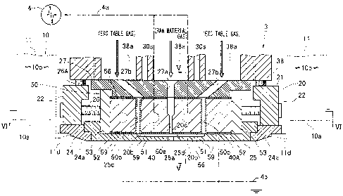
Next, the nozzle part 20 of the processing head 3 will be described.
As shown in FIG. 3, the nozzle part 20 comprises a nozzle body 21, an
electrode unit 50 received in the nozzle body 21, an insulative plate 27 for
covering this unit 50, base material opposing members 24, 25 disposed at
a lower side of the unit 50. As shown in FIG. 6, the nozzle body 21
includes metal-made left and right side frames 22 extending long in the
back and forth direction, and insulative resin-made front and rear side
frames 23 which are disposed between the front and rear end parts of the
side frames 22, respectively. The nozzle body 21 has a box-like
configuration which is long in the back and forth direction. The side
frame 22 is jointed to the lowermost-stage plate 38 of the gas uniformizing
part 30 by a bolt 26A (FIG. 30).
As shown in FIGS. 3 and 7, the lower frame 24 constituting one
element of the base material opposing member is made of metal such as
stainless and aluminum, and it has a rectangular configuration extending
in the back and forth direction. As mentioned above, the lower frame 24
is supported in such a manner as to be hooked on inner flanges 11d, 12d of
the housing 10. The side frames 22 are placed on the lower arm 24.
Although the lower arm 24 and the side frames 22 are merely contacted
and not jointed with each other, they may be jointed through an easy
removably attaching mechanism such as a bolt and a hook.
As shown in FIG. 3, a step 24a is formed on an inner peripheral
edge of the lower frame 24. A peripheral edge part of the rectangular
lower plate 25 constituting a main element of the base material opposing
member is placed and supported on this step 24a in such a manner as to be
hooked thereon. The lower plate 25 is composed of a ceramic (dielectric
CA 02471987 2006-03-07
34
member or insulative member) such as, for example, alumina. An
electrode receiving recess 25c is formed in an upper surface of the lower
plate, 25. The electrode unit 50 is fitted to this receiving recess 25c.
As shown in FIGS. 3 and 5, a more shallow recess 25d is disposed
at the receiving recess 25c formed in the upper surface of the lower plate
25. The recess 25d is wide, and it extends in the back and forth direction.
As shown in FIG. 3, a blowoff passage 25a extending from the recess 25d
to the lower surface is formed in a central part in the left and right
direction of the lower plate 25. As shown in FIG. 7, the blowoff passage
25a has a slit-like configuration, and it extends in the back and forth
direction.
As shown in FIG. 3, the insulative plate 27 composed of a ceramic
(insulative member) is vertically sandwiched between the lowermost-stage
plate 38 of the gas uniformizing part 30 and the electrode unit 50. The
insulative plate 27 is formed with three gas guide passages 27b, 27a, 27b
which extend generally over the entire length in the longitudinal direction
and separately arranged in the left and right direction. The central raw
gas guide passage 27a vertically pierces through the insulative plate 27.
The right side excitable gas guide passage 27b is slanted leftward from the
upper surface of the insulative plate 27 toward downward direction and it
finally reaches a lower surface of the plate 27. The left side excitable gas
guide passage 27b is slanted rightward from the upper surface of the
insulative plate 27 toward downward direction, and it finally reaches the
lower surface of the plate 27.
As shown in FIGS. 3 and 6, the electrode unit 50 comprises an
electrode group consisting of four (a plurality of) electrodes 51, 52, a pair
of left and right side plates 53, and a pair of front and rear end plates 54.
Each of the electrodes 51, 52 is constituted by providing an arc preventive
solid dielectric layer 59 to the surface of a main body 56 made of metal
such as aluminum and stainless steel. The metal main body 56 has a
CA 02471987 2004-06-25
vertically long square configuration in section and extends long in the
back and forth direction. The solid dielectric layer 59 is composed of a
dielectric member such as ceramic and coated in the form of film on a
surface on the side of a flow passage 50b, as later described, and upper
and lower surfaces of the metal main body 56 by thermally sprayed
coating or the like. Instead of thermally sprayed coating, a resin sheet
such as poly-tetrafluoro-ethylene may be adhered to the metal main body
56.
The four electrodes 51, 52 are arranged in mutually parallel
relation in the left and right direction.
In the electrode group, the two electrodes 51 on the middle side are
electric field impressing electrodes (first electrodes), and the two
electrodes 52 on both left and right ends (both ends in the arranging
direction) are ground electrodes (second electrodes). Accordingly, the
electrode group is constituted by arranging the ground electrode 52, the
electric field impressing electrode 51, the electric field impressing
electrode 51 and the ground electrode 52 in this order in the left and right
direction.
Each of the electrodes 51, 52 may be formed therein with a
temperature controlling passage for allowing a temperature controlling
cooling water to pass therethrough.
The side plates 53 of the electrode unit 50 are each made of an
insulative resin. The side plates 53 are placed along rear surfaces
(reversed side surfaces of the opposing side with respect to the electrode
51) of the left and right electrodes 52 and sandwich the electrode group
from the left and right sides. A bolt 26 screwed in through the side frame
22 is abutted with a rear surface of the side plate 53. Owing to this
arrangement, the electrode unit 50 is correctly positioned and retained
within the nozzle body 21.
The end plates 54 of the electrode unit 50 are each made of an
CA 02471987 2004-06-25
36
insulative resin. The end plates 54 are applied to both end faces in the
longitudinal direction of the four electrodes 51, 52 and sandwich the
electrode group from the front and rear side.
A feeding/grounding structure of the electrodes 51, 52 will be
described. As shown in FIG. 6, a feed pin 40 is embedded in, for
example, a front end part (one end part in the longitudinal direction) of
each of the two electric field impressing electrodes on the middle side, and
a ground pin 40A having the same construction as the feed pin 40 is
embedded in a rear end part (the other end part in the longitudinal
direction) of each of the two electrodes 52 on both the left and right sides.
As shown in FIG. 10, the feed pin 40 for the electric field
impressing electrode 51 comprises a shaft-like pin main body 41 having a
shaft hole 41a which is open to a forward end face, a barrel body 42
received in the shaft hole 41a, and a core member 43 slideably received in
this barrel body 42. The pin main body 41, the barrel body 42 and the
core member 43 are composed of a conductive metal such as stainless
steel and they are electrically conducted by being abutted with one another
at their inner and outer peripheral surfaces.
A forward end part of the pin main body 41 is withdrawably
pushed into a pin hole 56a formed in a front end face of the electric field
impressing electrode 51. Owing to this arrangement, the pin main body
41 and the electrode 51 are electrically conducted with each other. A
coiled spring 44 (biasing means) is received in the barrel body 42. By
this coiled spring 44, the core member 43 is biased in the forward end
direction, i.e., in the direction to be pushed out of the shaft hole 41 a.
Owing to this arrangement, the forward end part of the core member 43 is
pressed hard against the innermost end face of the pin hole 56a. As a
result, the electrically conducting state between the feed pin 40 and the
electrode main body 56 is surely maintained.
Barrel-like pin holders 45A, 45B, which are each made of an
CA 02471987 2004-06-25
37
insulative member are mounted on a basal end part (head part) of the pin
main body 41. The basal end part of the holder-mounted pin main body
41 projects from the end plate 54 and is disposed between the front side
end plate 54 and the side frame 23. As shown in FIG. 5, a power feed
line 4a extends from the basal end part of this main body 41 and is
connected to the pulse power source 4.
The ground pin 40A for the ground electrode 52 has the same
construction as the feed pin 40. As shown in FIG. 6, the head part of the
ground pin 40A projects from the rear side end plate 54. A ground line
4b is connected to the head part of the ground pin 40A. The ground line
4b is allowed to pass between the upper surface of the rear-side side frame
23 and the insulative plate 27 and pulled outside of the processing head 3
so as to be grounded.
As shown in FIGS. 3 and 6, flow passages 50a, 50b for the
processing gas, i.e., the raw material gas or excitable gas are formed
between the adjacent electrodes 51, 52.
More specifically, between the middle side electrodes 51, 51
having the same polarities, the flow passage 50a for the raw material gas is
formed. Between both the left and right side electrodes 52, 51 having
different polarities, one each of the flow passages 50b (plasma discharge
space) for the excitable gas is formed. Accordingly, the excitable gas
flow passage 50b, the raw material gas flow passage 50a, and the excitable
gas flow passage 50b are arranged in this order from the left.
The electrode unit 50 is provided at the front and rear end plates 54
with three plate piece-like spacers 55 which are each made of an insulative
resin. Those plate piece-like spacers 55 are pushed in between the
adjacent electrodes 51, 52, thereby establishing the width of each of the
flow passages 50b, 50a, 50b.
As shown in FIG. 3, an upper end part (upstream end) of the
central flow passage 50a is straightly continuous with the gas uniformizing
CA 02471987 2004-06-25
38
passage 30x in the central region 30A of the gas uniformizing part 30
through the central guide passage 27a of the insulative plate 27, and thus
with the raw material gas source 1 through the tube la.
The surface for forming the flow passage 50a of each electric field
impressing electrode 51 is indented at an upper side thereof and projected
at a lower side thereof. A step is formed at an intermediate part of the
flow passage forming surface. Owing to this arrangement, the flow
passage 50a is enlarged in width at the upper side and reduced in width at
the lower side.
Upper end parts (upstream ends) of the flow passages 50b, 50b on
the left and right sides are continuous with the gas uniformizing passages
30x, 30x in the left and right regions 30B, 30B of the gas uniformizing
part 30 through the left and right guide passages 27b, 27b of the insulative
plate 27, and thus, with the excitable gas source 2 through the tube 2a.
Each ground electrode 52 is placed on an upper surface of the
electrode receiving recess 25c of the lower plate 25. On the other hand,
as shown in FIGS. 3 and 5, the respective electric field impressing
electrodes 51 are spacedly arranged at an upper part of the recess 25d of
the lower plate 25. Owing to this arrangement, a gap 20b is formed
between the lower surface of each electric field impressing electrode 51
and the lower plate 25.
As shown in FIG. 3, those left and right gaps 20b each serve as a
communication passage for communicating the flow passage 50b between
the electrodes having different polarities with the flow passage 50a
between the electrodes having the same polarities. That is, a left end part
(upstream end) of the left side communication passage 20b is continuous
with the flow passage 50b between the electrodes having different
polarities, and a right end part (downstream end side) is crossed with the
lower end part (downstream end) of the electrode passage 50a between the
electrodes having the same polarities. The right end part (upstream end)
CA 02471987 2004-06-25
39
of the right side communication passage 20b is continuous with the flow
passage 50b between the right side electrodes having different polarities,
and the left end part (downstream end) is crossed with the downstream end
of the flow passage 50a between the electrodes having the same polarities.
The flow passage 50a between the electrodes having the same
polarities constitutes the "first flow passage", and the flow passage 50a
between the electrodes having different polarities and the communication
passage 20b constitutes the "second flow passage".
The electrodes 51, 51 having the same polarities constitute the
"first flow passage forming means". The electrodes 51, 52 having
different polarities, and the electrode 51 and the lower plate 25 constitute
the "second flow passage forming means".
The left and right communication passages 20b are horizontal and
orthogonal to the vertical first flow passage 50a. The left and right
second flow passages 50b, 20b are symmetrical with each other with
respect to the central first flow passage 20a sandwiched therebetween.
As shown in FIG. 8 on an enlarged basis, the blowoff passage 25a
of the lower plate 25 is continuous with a crossing part (converging part)
among the three flow passages 20b, 50a, 20b. This blowoff passage 25a
serves as a common blowoff passage of the raw material gas and the
excitable gas, and its downstream end (blowoff port) is open to a lower
surface of the lower plate 25. The blowoff passage 25a is disposed right
under the vertical flow passage 50a.
Operation of the normal pressure plasma film forming apparatus
M1 thus constructed will now be described.
The Excitable gas (second gas) such as hydrogen coming from the
excitable gas source 2 is introduced, via the gas tube 2a, into the gas
uniformizing passages 30x in the left and right regions 30B from two left
and right plugs 32P of the processing head 3 and uniformized in the back
and forth longitudinal direction by those passages 30x. The excitable gas
CA 02471987 2004-06-25
thus uniformized is introduced into the left and right flow passages 50b via
the left and right guide passages 27b, respectively.
On the other hand, the voltage coming from the pulse power source
4 is fed to the electric field impressing electrode 51, and a pulse electric
field is impressed between the electrodes 51, 52 having different polarities.
By this, as shown in FIG. 8, Glow discharge is generated in the left and
right flow passages 50b, and the excitable gas is plasmatized (excited and
activated). The excitable gas thus plasmatized is guided into the
communication passage 20b from the flow passage 50b and allowed to
flow toward the crossing part 20c. This excited gas itself does not
contain any component which is adhered to and deposited on the surface
of ceramic or the like by excitation. Accordingly, it never happens that
film is adhered to the opposing surfaces between the electrodes 51, 52
having different polarities, the lower surface of the electrode 51 and the
upper surface (second flow passage forming surface) of the lower plate 25.
Simultaneously with the flowing of the excitable gas, the raw
material gas (first gas) such as silane gas coming from the raw material
gas source 1 is introduced, via the gas tube la, into the gas uniformizing
passage 30x in the central region 30A from the central gas plug 32P of the
processing head 3 and uniformized in the back and forth longitudinal
direction. Thereafter, the gas is introduced, via the central guide passage
27a, into the central flow passage 50a between the electrodes having the
same polarities. Although pulse voltage is fed to each of the two electric
field impressing electrodes 51, no electric field is impressed between those
electrodes 51, 51 having the same polarities and therefore, it never
happens that plasma discharge occurs at the flow passage 50a. Thus, the
raw material gas is allowed to pass as it is without being plasmatized.
For this reason, a film is not adhered to the opposing surfaces (first flow
passage forming surface) between the electrodes 51 having the same
polarities.
CA 02471987 2004-06-25
41
Since no film is attached to anywhere of the four electrodes,
maintenance of the electrodes 51, 52 becomes easy. Moreover, loss of
the raw material occurrable at the time of passage between the electrodes
can be eliminated.
The raw material gas passing through the flow passage 50a is
reduced at the lower side of the passage 50a where the passage 50a is
narrow and therefore, the pressure is increased.
After passing through the central flow passage 50a, the raw
material gas flows to the crossing part 20c between the left and right
communication passages 20b. The excitable gas plasmatized in the left
and right flow passages 50b also flows to the crossing part 20c through the
communication passage 20b. By this, the raw material gas is contacted
with the plasmatized excitable gas (active species) so as to take place such
reaction as decomposition and excitation, thereby generating a radical
reaction production p which is turned out to be a film.
The excitable gas flow entering the crossing part 20c from the left
and right passages 20b is pushed by the raw material gas flow and curved
downward. By this, the excitable gas mostly flows along the right side
edge surface and the left side edge surface of the blowoff passage 25a, and
the raw material gas mostly flows in such a manner as being sandwiched
between the left and right excitable gas flows and passes through the
middle side of the blowoff passage 25a. This makes it possible for the
reaction product p scarcely to contact the edge surface of the blowoff
passage 25a. Therefore, adhesion of a film to the edge surface of the
blowoff passage 25a can be reduced, and the raw material loss can further
be reduced.
Then, the processing gas (excitable gas and raw material gas) is
blown off from the blowoff passage 25a generally in a laminar flow state.
By this, a desired film A can be formed by applying the reaction product p
to the upper surface of a base material W placed immediately under the
CA 02471987 2004-06-25
42
blowoff passage 25a.
Since the gas is uniformized in the back and forth direction by the
gas uniformizing part 30, the film A, which is uniform in the back and
forth direction, can be formed.
Thereafter, the processing gas flows in the two left and right
directions through the space between the processing head 3 and the base
material W in such a manner as to be away from the blowoff passage 25a.
At that time, the excitable gas is mostly one-sided toward the processing
head 3 side, and the raw material gas is mostly one-sided toward the base
material W side located thereunder. By this, the reaction product p can
be maintained in a state hardly contacting the lower surfaces of the lower
plate 25 and the lower frame 24. As a result, film adhesion to those
members 25, 24 can be reduced, and frequency of film removal can be
reduced.
The processed gas is taken into the housing 10 through the intake
port l0a and then discharged by actuation of a vacuum pump 14. By
controlling the intake pressure of this vacuum pump 14, etc., the excitable
gas and the raw material gas can be maintained in the generally laminar
flow state, and film adhesion to the processing head 3 can more surely be
prevented from occurring.
For example, even if a film should be formed on the base material
opposing member (lower frame 24 and lower plate 25), by pulling out
processing head 3 and taking it out of the housing 10 as shown in FIG. 9,
only the base material opposing members 24, 25 would left remained in
the state hooked on the inner flanges l ld, 12d of the housing 10. By this,
the base material opposing members 24, 25 can be separated from the
processing heads 3 very easily. Thereafter, only the base material
opposing members 24, 25 are subjected to cleaning process by being
dipped in a chemical liquid such as, for example, strong acid, so that a
film can be removed. Since the entire processing head 3 is no more
CA 02471987 2004-06-25
43
required to be subjected to cleaning process, maintenance can be
simplified. On the other hand, by preparing spare parts of the base
material opposing members 24, 25 and attaching them to the apparatus M1,
the film forming processing can be kept continued even during the
cleaning process.
According to the normal pressure plasma film forming apparatus
Ml, since the power feed line 4a is pulled out of one end part of the
processing head and a ground line 4b is pulled out of the other end part
(FIGS. 5 and 7), those lines 4a, 4b can be prevented from being short-
circuited.
Moreover, the power feed/ground lines 4a, 4b and the electrode
main body 56 can be electrically connected through the power feed/ground
pins 40, 40A surely and easily. Since the power feed/ground pins 40,
40A can easily be removed, they can not be any disturbance at the time of
maintenance.
Moreover, the two ground electrodes 52 are arranged on the left
and right outer sides with the two electric field impressing electrodes 51
sandwiched therebetween, electric field can be prevented from leaking
outside and the entire processing head 3 can easily be grounded, too.
Other embodiments of the present invention will be described next.
In the embodiments to be described hereinafter, the same construction as
in the above-mentioned embodiment is denoted by same reference
numeral in Figures so that description thereof can be simplified.
FIGS. I l and 12 show a second embodiment of the present
invention. In the second embodiment, the blowoff ports for the first and
second gases are separately formed.
More specifically, as shown in FIG. 12, a lower plate 25 is formed
with three slit-like individual blowoff passages 25b, 25a, 25b which
extend in the back and forth direction and which are arranged in parallel at
equal intervals in the left and right direction.
CA 02471987 2004-06-25
44
As shown in FIG. 11, the left side blowoff passage 25b is
continuous straight with a lower part of a flow passage 50b between the
left side electrodes 52, 51 having different polarities. The central
blowoff passage 25a is continuous straight with a lower part of a flow
passage 50a between the central electrodes 51, 51 having the same
polarities. The right side blowoff passage 25b is continuous straight with
a lower part of the flow passage 50b between the right side electrodes 51,
52 having different polarities. The lower end parts of those three blowoff
passages 25b, 25a, 25b are open to a lower surface of the lower plate 25.
The lower end opening of the central blowoff passage 25a constitutes a
blowoff port for a raw material gas (first gas), and the lower end openings
of the left and right blowoff passages 25b constitute blowoff ports for an
excitable gas (second gas).
The lower plate 25 is not provided at an electrode receiving recess
25c with the recess 25d of the first embodiment, and an electric field
impressing electrode 51 is abutted with the upper part of the receiving
recess 25c. Accordingly, the communication passage 20b of the first
embodiment is not formed.
The raw material gas guided into the central flow passage 50a is
blown off directly through the blowoff passage 25a, and thereafter,
allowed to flow separately in the two left and right directions between the
lower plate 25 and a base material W. On the other hand, the excitable
gas guided into the left and right flow passages 50b is plasmatized (excited
and activated) by the electric field between the electrodes 51, 52 having
different polarities, and thereafter, blown off through the left and right
blowoff passages 25b. The raw material gas flowing on the base material
W contacts the excitable gas thus blown off. As a result, reaction is
taken place. By this, a film A is formed on the base material W.
Thereafter, the excitable gas and the raw material gas flow toward an
intake port 10a in their vertically overlapped generally laminar flow states
CA 02471987 2006-03-07
and then, they are discharged.
FIG. 13 shows a third embodiment of the present invention.
In the third embodiment, an electrode group consisting of eight (a
plurality of) planar electrodes 51, 52 is disposed within a metal conductor-
made nozzle body 20B of a processing head 3. Those electrodes are in
mutually parallel relation and arranged at equal intervals in the order of
the ground electrode 52, the electric field impressing electrode 51, the
ground electrode 52, the ground electrode 52, the electric field impressing
electrode 51, the electric field impressing electrode 51 and the ground
electrode 52 from left. Owing to this arrangement, the second flow
passages (plasma discharge space) 50b between the electrodes having
different polarities and the first flow passages 50a between the electrodes
having the same polarities are alternately arranged. Each first flow
passage 50a allows the raw material gas (first gas) from a raw material gas
source (not shown) to pass therethrough, and each second flow passage
50b allows the excitable gas (second gas) from an excitable gas source
(not shown) to pass therethrough.
The ground electrodes 52 located at the opposite end parts in the
arranging direction of the electrode group are abutted at their rear surfaces
along a nozzle body 20B and electrically conducted with this nozzle body
20B. Although not shown specifically, the central side two ground
electrodes 52 are abutted at opposite end parts in the longitudinal
direction (orthogonal direction to the paper surface of FIG. 13) with the
nozzle body 20B and electrically conducted with this nozzle body 20B.
The nozzle body 20B is grounded through the ground line 4b. Owing to
this arrangement, the entire processing head 3 can be grounded and at the
same time, the ground electrode 52 can be grounded.
In the third embodiment, the ground electrodes 52 located at the
opposite outer sides may be integrally formed with the nozzle body 20B.
That is, the nozzle body 20B may serve also as the ground electrodes 52
CA 02471987 2004-06-25
46
located at the opposite outer sides.
In the third embodiment, the number of the electrodes in the
electrode group is not limited to eight but it may be three, five to seven, or
nine or more. Those electrodes are arranged such that different polarities
space (second flow passage) for allowing the second gas to pass
therethrough and the same polarities space (first flow passage) for
allowing the first gas to pass therethrough are alternately formed. That is,
those electrodes are arranged in the order of the second electrode, the first
electrode, the first electrode, the second electrode, the second electrode,
the first electrode, the first electrode, the second electrode, the second
electrode, the first electrode, the first electrode, the second electrode and
so on. The second electrode as the ground electrode is preferably
arranged at the outermost side. In case the number of the electrodes is
even in total, the number of the first electrodes is equal to the number of
the second electrodes. In case the number of the electrodes is odd in total,
the number of the second electrodes becomes larger than the number of
the first electrodes by one. It is accepted that the electrodes having the
same polarities (preferably, ground electrodes) are arranged at the
outermost side and at an inner location next to the outermost side, and the
first gas is passed through the opposing space at the outermost side. It is
also accepted that a plurality of first and second electrodes, which are so
long as almost equal to the entire length of a base material having a large
area, are arranged over the entire width of the base material in the above-
mentioned order so that the entire base material can be formed with a film
at a time.
Moreover, the first and second flow passages may be alternately
arranged one by one. It is also accepted that a plurality of at least one of
the first and second flow passages are arranged adjacent to each other, and
groups of such adjacent flow passages and the other flow passages are
alternately arranged in parallel.
CA 02471987 2004-06-25
47
FIG. 14 shows a modified embodiment of such an alternate
arrangement construction. The processing head 3 of this modified
embodiment, a group of electrodes are arranged in the order of the second
electrode 52, the first electrode 51, the second electrode 52, the second
electrode 52, the first electrode 51 and the second electrode 52. Owing
to this arrangement, one of such first flow passages 50a is arranged at the
center and two of such second flow passages 50b are arranged on the
opposite left and right sides thereof. That is, two (a plurality of) second
flow passages 50b and one first flow passage 50a are alternately arranged
in parallel. In FIG. 14, the ground line of the second electrode 52 is not
shown.
According to the modified embodiment of FIG. 14, a large reaction
area for reaction of the raw material gas and the plasmatized excitable gas
can be obtained, the raw material gas can sufficiently be reacted to form
into a film and the reaction efficiency (yield) can be enhanced. Moreover,
by mildly blowing off the plasmatized excitable gas from the respective
second flow passages 50ab, a generally laminar flow state can surely be
obtained.
FIGS. 15 through 20 show a fourth embodiment of the present
invention.
In the fourth embodiment, as in the first embodiment, second flow
passages are arranged on the left and right sides with a central first flow
passage sandwiched therebetween. Those three flow passages are
converged and continuous with a single common blowoff passage 25a.
The fourth embodiment is different from the first embodiment in respect
of the arrangement position of the ground electrode and the location of the
plasma discharge part of the second flow passage.
More specifically, as shown in FIGS. 15 and 17, in the processing
head 3 of the fourth embodiment, dummy electrode spacers 52S instead of
the ground electrodes 52 of the first embodiment are disposed at the
CA 02471987 2006-03-07
48
locations for receiving the ground electrodes 52=of the first embodiment
(FIGS. 3 and 6). The dummy electrode spacers 52S each have a
substantially same configuration as the ground electrodes 52 of the first
embodiment, but they are composed of an insulative member (dielectric
member) such as ceramic instead of conductive metal. Accordingly, the
flow passage 50b between the dummy electrode spacer 52S and the
electric field impressing electrode 51 does not serve as a plasma discharge
space. The excitable gas is allowed to pass through the flow passage 50b
without being plasmatized.
A lower plate 25 of the fourth embodiment has not only the
function as a base material opposing member or blowoff port constituting
member of the processing head 3 but also the function as a retaining
member for the ground electrode. That is, as shown in FIGS. 15 and 18,
a pair of shallow receiving recesses 25e are formed in a lower surface of
the lower plate 25 with a common blowoff passage 25a sandwiched
therebetween. The recesses 25e extend in the back and forth direction.
A ground electrode 52A composed of an elongate thin metal conductive
plate is fitted to each receiving recess 25e. Owing to this arrangement,
the ground electrodes 52A are arranged in opposing relation at the side
(lower side) which is to be faced with the base material W of the electric
field impressing electrode 51. Accordingly, the communication passages
20b between the two electric field impressing electrodes 51 and the lower
plate 25 serve as the plasma discharge spaces, respectively.
As shown in FIG. 20, plasma PL is disposed not only at the inside
of the communication passage 20b but also overflowed to the crossing part
20c.
In the lower plate 25 composed of a dielectric member such as
alumina, the part covering the upper surface of the metal-made ground
electrode 52A and the part (i.e., blowoff passage 25a forming part) along
the end face on the blowoff passage 25a side of the ground electrode 52A
CA 02471987 2006-03-07
49
have a role acting as a solid dielectric layer of the ground electrode.
As shown in FIG. 20, the right side end face facing the common
blowoff passage 25a of the left side ground electrode (metal main body)
52A is flush with the same side end face (right side end face) of the metal
main body 56 of the left side electric field impressing electrode 51. The
left side end face facing the common blowoff passage 25a of the right side
ground electrode (metal main body) 52A is flush with the same side end
face (left side end face) of the metal main body 56 of the right side electric
field impressing electrode 51. The end face on the common blowoff
passage 25a side of the respective ground electrodes 52A may be
expanded from the same side end face of the electric field impressing
electrode main body 56.
As shown in FIG. 15, the end face on the opposite side to the
common blowoff passage 25a side of each ground electrode 52A is
projected from a rear surface of the electric field impressing main body
56.
As shown in FIG. 16, the opposite end edges in the longitudinal
direction of the ground electrode 52A are in contact with the lower frame
24 composed of a metal conductor. A ground line 4b is allowed to
extend from the rear end part (opposite side to the arrangement side of the
power feed pin 40) of the lower frame 24 and grounded.
The ground electrode 52A may be constituted by forming a slit,
which serves as the blowoff passage 25a, in a single elongate metal
conductive plate.
The fourth embodiment is also different from the first embodiment
in respect of the solid dielectric layer construction of the electrode 51.
That is, as shown in FIG. 19, the solid dielectric layer of the
electric field impressing electrode 51 in the fourth embodiment is
composed of a case 57 which is separately formed from the electrode main
body 56 instead of a thermally sprayed film 59 (FIG. 3) which is integrally
4
CA 02471987 2006-03-07
thermally sprayed on the electrode main body 56. The case 57 includes a
case main body 57a composed of ceramic (dielectric member) such as
alumina and glass, and a lid 57b composed, of the same material as the
case main body 57a. The case 57 extends long in the back and forth
direction.
The case main body 57a includes an internal space of the same
configuration as the electrode main body 56. The case main body 57a is
open to a rear surface (surface on the opposite side to the opposing side of
the other electrode 51) thereof. The electrode main body 56 is
removably received in the internal space of the case main body 57a. The
rear surface of the case main body 57a is blocked with the lid 57b.
Owing to this arrangement, the entire surface of the electrode main body
56 is covered with the solid dielectric layer composed of the case 57.
The lid 57b is in removable relation with the case main body 57a.
The case main body 57a is formed, for example, at a front side end
plate thereof with a hole 57c for allowing a power feed pin 40 to be
inserted therein.
The plate on the side opposing the other electrode 51 in the case
main body 57a of each electric field impressing electrode 57a is thin at the
upper side, thick at the lower side and formed at the intermediate part with
a step. Owing to this arrangement, the flow passage 50a between the pair
of electrodes 51 is wide in width at the upper side and narrow in width at
the lower side.
According to the fourth embodiment, the excitable gas coming
from an excitable gas source 2 is not plasmatized in the left and right flow
passages 50b, 50b but it is plasmatized (excited and activated) in
communication passages 20b, 20b which are located next to the passages
50b, 50b. Since the excitable gas does not contain any film forming
component, a film is not adhered to the lower surface of the electrode 51
or to the upper surface (communication passage 20b forming surface) of
CA 02471987 2004-06-25
51
the lower plate 25.
As shown in FIG. 20, the excitable gas plasmatized in the left and
right communication passages 20b flows to a crossing part 20c. Also, the
raw material gas coming from the raw material gas source I enters the
crossing part 20c via the central flow passage 50a. Owing to this
arrangement, the film raw material is reacted with the plasmatized
excitable gas to generate a reaction product p which forms a film. In
addition, the raw material gas also passes through the plasma PL which is
overflowed to the crossing part 20c (the raw material gas flows very near
the plasma discharge space). By this, the raw material gas can be
plasmatized directly and more reaction products p can be obtained. As a
result, film forming efficiency onto the base material W can be enhanced.
Since a ground electrode 52A (grounded conductive member) is
interposed between the electric field impressing electrode 51 and the base
material W, arch can be prevented from falling onto the base material W
and thus, the base material W can be prevented from being damaged.
Moreover, since the end face on the side facing the common
blowoff passage 25a of the ground electrode 52A is flush with the same
side end face of the electric field impressing electrode main body 56,
electric field can be prevented from leaking downward from the side end
face of the common blowoff passage 25a of the ground electrode 52A and
arc can more surely be prevented from falling onto the base material W.
Thus, the processing head 3 can be brought close to the base material W
and thus, the distance (working distance) between the processing head 3
and the base material W can be reduced sufficiently and thus, the working
distance can be made shorter than the short deactivating distance (for
example, 2 mm) of radical under normal pressure. Thus, the base
material W can surely be brought into place before the reaction product p
is deactivated. As a result, a film can be formed at a high-speed and
reliably.
CA 02471987 2004-06-25
52
Since the electric field impressing electrode main body 56 is
entirely enclosed in a case 57 as a solid dielectric layer, abnormal electric
discharge can more surely be prevented from occurring.
In case a film is adhered to the case 57 of the electric field
impressing electrode 51, the electrode 61 is removed from the nozzle body
21 for decomposition. At the time of decomposition, the power feed pin
40 can easily be withdrawn. Removing the lid 57b from the case main
body 57a, the electrode main body 56 can easily be taken out. Since a
film is adhered only to the case 57, for example, only the case 57 is
replaced and the electrode main body 56 is put into a new case. By doing
so, it is no more required to prepare a plurality of electrode main bodies 56.
The work for putting the main body 56 into a new case is also easy.
On the other hand, with respect to the film-adhered case 57,
attempt is made to remove the film from the case 57 by dipping the case
57 in a strong acid, or by any other suitable means. This makes it
possible to re-use the case 57, thus resulting in elimination of the waste of
materials. Since the case 57 is separately formed for each electrode 51,
the work of maintenance can be conducted separately.
By composing the dummy electrode spacer 52S from a metal
conductor instead of a dielectric member and grounding the same, the
spacer 52S can be used as a ground electrode part together with the planar
electrode 52A. By doing so, the entire second flow passages 50b, 20b
can serve as a plasma discharge space. In this case, the ground electrode
52S may be of the same dielectric case receiving construction as the
electric field impressing electrode 51.
In the individual blowoff construction of the second embodiment
(FIG. 11), each of the four electrodes 51, 52 may be of dielectric case
receiving construction.
FIG. 21 shows a modified embodiment of the ground electrode
construction in the fourth embodiment.
CA 02471987 2004-06-25
53
In this modified embodiment, the end face on the side facing the
common blowoff passage 25a of each ground electrode (metal main body)
52A is set back from the same side end face of the metal main body 56 of
the electric field impressing electrode 51. The common blowoff passage
52a forming surface of the lower plate 25 is generally flush with the same
side end face of the electric field impressing main body 56. However,
the present invention is not limited to this. Instead, the common blowoff
passage 25a forming surface may be indented near to the end face of the
ground electrode 52A. That is, the width of the common blowoff
passage 25a may be increased approximately to the distance between the
opposing end faces of the left and right ground electrodes 52A.
According to this modified embodiment, a lateral electric field is
formed by displacement between the electric field impressing electrode
main body 56 and the ground electrode main body 52A. This lateral
electric field causes the plasma PL to move around the lower side of the
expanding part 25H from the electrode 52A of the lower plate 25. 4wing
to this arrangement, further reaction of the raw material gas can be taken
place at a location nearer to the base material W, and thus, a film can be
formed at a higher speed and reliably.
The entire surface of the ground electrode main body 52A is
coated with a thin dielectric member 59A separately by suitable means.
Owing to this arrangement, abnormal electric discharge can more surely
be prevented from occurring.
FIG. 22 shows a fifth embodiment of the present invention.
A processing head 3X of the fifth embodiment includes an electric
field impressing electrode 51X composed of a metal conductor, and a
ground electrode (grounded conductive member) 52X covering a lower
part (side to be faced with the base material W) of the electrode 51X. A
solid dielectric member 28 composed of ceramic or the like is loaded
between the upper and lower electrodes 51X, 52X. The solid dielectric
CA 02471987 2004-06-25
54
member 28 is a solid dielectric layer which is common to the two
electrodes 51X, 52X. By this solid dielectric member 28, the two
electrodes 51X, 52X are electrically isolated. A cutout part 52b is
formed at a central part of the ground electrode 52X. A lower surface of
the solid dielectric member 28 is exposed from this cutout part 52b.
Tip parts of two blowout nozzles 61, 62 are arranged at the side of
the ground electrode 52X. A basal end part of the raw material gas
blowoff nozzle 61 (first flow passage forming means) is continuous with a
raw material gas source 1 through a raw material gas tube la, and a basal
end part of the excitable gas blowoff nozzle 62 (second flow passage
forming means) is continuous with an excitable gas source 2 through an
excitable gas source 2 through an excitable gas tube 2a. The blowoff
shafts at the tips of those blowoff nozzles 61, 62 are diagonally disposed
toward a space between the ground electrode 52X and the base material W.
Moreover, the excitable gas blowoff nozzle 62 is disposed at an upper side
(nearer to the ground electrode 52X) of the raw material gas blowoff
nozzle 61.
According to the fifth embodiment, the excitable gas is blown off
into a space between the ground electrode 52X and the base material W
from the upper side nozzle 62, and at the same time, the raw material gas
is blown off into the same space from the lower side nozzle 61. At that
time, a generally laminar flow is formed in which the excitable gas is one-
sided to the upper side and the raw material gas is one-sided to the lower
side. The upper side excitable gas flows into the cutout part 52b.
On the other hand, a lateral electric field is taken place in the
cutout part 52b by pulse voltage impression of the pulse power source 4.
By this, the inside of the cutout part 52b serves as a plasma discharge
space, and the excitable gas flown into the cutout part 52b is plasmatized
(excited and activated). The raw material gas contacts this plasmatized
excitable gas. Or the raw material gas flows very near the plasma
CA 02471987 2004-06-25
discharge space 52b. By this, the raw material gas can be reacted right
near the base material W, and a film A can be formed at a high speed and
reliably. Since the excitable gas flow comes nearer to the ground
electrode 52X side than the raw material gas does even after the excitable
gas passes through the plasma discharge space 52b, adhesion of a film to
the lower surface of the ground electrode 52X, i.e., the lower surface of
the processing head 3X can be prevented or restrained.
Since the ground electrode 52X (grounded conductive member) is
interposed between the electric field impressing electrode 51X and the
base material W, arc can be prevented from falling onto the base material
W, and thus, the base material W can be prevented from being damaged.
FIG. 23 shows a sixth embodiment of the present invention.
In a processing head 3Y of the sixth embodiment, a paired electric
field impressing electrodes 51Y and ground electrodes 52Y are distantly
arranged leftward and rightward in opposing relation. A second flow
passage 20h serving as a plasma discharge space is vertically formed
between those electrodes 51Y, 52Y. A tube 2a extending from the
excitable gas tube 2 is connected to the upper end part (upstream end) of
the second flow passage 20h.
A conductive member 29 composed of a metal plate is disposed at
the lower end part of the processing head 3Y. The conductive member
29 is grounded through a ground line 4b. The conductive member 29
covers a lower side (side to be faced with the base material W) of the
electric field impressing electrode 51Y. An insulative member 28Y for
electrically isolating the electric field impressing electrode 51Y and the
conductive member 29 is loaded between the electrode 51Y and the
member 29.
A gap 20g serving as a first flow passage is horizontally formed
between the ground electrode 52Y and the conductive member 29. A
tube la extending from the raw material gas source 1 is connected to a
CA 02471987 2004-06-25
56
right end part (upstream end) of the first flow passage 20g. A left end
part (downstream end) of the first flow passage 20g is crossed with a
lower end part (downstream end) of the second flow passage 20h. The
conductive member 29 is formed with a blowoff passage 29a extending
from the crossing part 20c between the first and second flow passages 20g,
20h right thereunder. The blowoff passage 29a serves as a common
blowoff passage for the raw material gas and the excitable gas.
Also in the sixth embodiment, adhesion of a film to the plasma
discharge space forming surfaces of the electrode 51Y, 52Y, etc. can be
prevented from occurring, and arc can be prevented from falling onto the
base material W from the electric field impressing electrode 51Y.
FIG. 24 shows a modified embodiment of an electrode power
feeding/grounding construction. A covered conductor 46 serving as a
power feed line 4a or ground line 4b is constituted by covering a
conductive wire 46a with an insulative tube 46b. The coated conductor
46 is inserted in a hole 56d of an electrode main body 56 through a hole
57d of a dielectric case 57.
In the wire 46a of the covered conductor 46, only the terminal end
part located at the innermost side of the hole 56d is exposed from the
insulative tube 46b, and the part located on this side in the hole 56d is
covered with an insulative tube 46b. Of course, the wire 46a is covered
at a part thereof located in the hole 57d of the dielectric case 57 and at a
part thereof located outside the case 57 with the insulative tube 46b.
A screw (bolt) 47 is screwed into the electrode main body 56 in
such a manner as to be generally orthogonal to the hole 57d. By this
screw 47, the exposed tip part of the wire 46a is pressed against the inner
peripheral surface at the innermost end part of the hole 57d.
According to this construction, abnormal electric discharge from
the conductor 46 can surely be prevented from occurring. Moreover, the
terminal of the conductor 46 can surely be fixed to the electrode main
----- ----------
CA 02471987 2004-06-25
57
body 56, so that the former can surely be electrically conducted with the
latter. Moreover, at the time of maintenance such as replacement of the
dielectric case 57, the conductor 46 can easily be removed from the
electrode 51 by loosening the screw 47.
FIG. 25 shows a modified embodiment of the dielectric case
serving as a solid dielectric layer of an electrode.
In the dielectric case 57X of the modified embodiment, an opening
of the case main body 57a is formed on one end face in the longitudinal
direction, instead of the rear surface of the embodiment of FIG. 19. A
metal main body 56 of the electrode is inserted through this end face
opening. A lid 57b of the case 57X covers up the end face opening.
FIGS. 26 and 27 show another modified embodiment of a
dielectric case. A main body 58X of this dielectric case 58 is constituted
by combining a pair of pieces 58a, 58b each having an L-shaped
configuration in section. Those pieces 58a, 58b are formed at end edges
thereof with pawls 58c, 58d, respectively. By fitting the pawls 58c, 58d
with respect to each other, a long square-shaped case main body 58X is
formed. This case main body 58X is formed at opposite end parts thereof
in the longitudinal direction with openings 58e, respectively. A lid 58f is
removably disposed at each of those openings 58e.
FIG. 28 shows a further modified embodiment of an dielectric case.
In this modified embodiment, two (a plurality of) electrode dielectric cases
are integrally connected with each other. In other word, two (a plurality
of) electrode metal main bodies 56 are received in a single common
dielectric case 70.
The common dielectric case 70 comprises a single case main body
71 composed of a dielectric member, and two lids 74 composed of a
dielectric member. The case main body 71 includes two case main body
parts 72 horizontally extending long in mutually parallel relation, and a
connection part 73 for interconnecting the opposite end parts (only the
CA 02471987 2004-06-25
58
innermost side of the paper surface is shown in FIG. 28) of those main
body parts 72. The rear surfaces on the opposite side to the opposing
sides of those main body parts 72 are open. After the electrode metal
main bodies 56 are inserted in the main body parts 72 through those rear
surface openings, the rear surface openings are covered up by the lids 74,
respectively.
In this embodiment, one of the two electrodes is an electric field
impressing electrode connected to a power source 4, and the other is a
grounded ground electrode. However, the present invention is not
limited to this. Instead, they may be electrodes having the same
polarities.
A flow passage 70a (in this embodiment, a second flow passage
serving as a plasma discharge space) is formed between two main body
parts 72 of the common dielectric case 70. The flow passage 70a extends
long in the same direction as the main body part 72. After being
uniformized in the longitudinal direction, the processing gas (excitation
gas in this embodiment) is guided into the upper end opening (upstream
end) of the flow passage 70a. The lower end opening of the flow passage
70a serves as a blowoff port.
The dielectric case 70 constitutes a second flow passage forming
means. The first flow passage forming means is not shown (the same is
true also in FIGS. 29 through 33).
The upper side parts 72c of the opposing side plates (i.e., solid
dielectric layer on the opposing side of two electrodes) in two main body
parts 72 are relatively thin, and the lower side parts 72d are relatively
thick.
A step 72g is formed at an intermediate height. Owing to this
arrangement, the upper side of the flow passage 70a is large in width and
the lower side is small in width as in the case with first embodiment (FIG.
3).
The flow passage 70a is made to serve as a plasma discharge space
CA 02471987 2004-06-25
59
by electric field impression of the pulse power source 4. This plasma
becomes relatively strong at the upper side (upstream side) of the step 72g
and relatively weak at the lower side (downstream side) due to difference
in thickness between the upper and lower plate parts 72c, 72d serving as
the solid dielectric layer. As apparent from the foregoing description, the
state of plasma can be varied by changing the thickness of the dielectric
case.
The upper and lower plate parts 72c, 72d serving as the solid
dielectric layer may be reversed in thickness in according with the
purpose.
In the embodiment of FIG. 28, since the dielectric cases of the two
electrodes are integrally formed, the number of parts can be reduced.
Moreover, the labor and time required for assembling the two electrodes
can be eliminated, relative positioning of the electrodes can be made easily
and correctly, and the shape dimension of the flow passage 70 can be
enhanced in precision.
The dielectric case construction itself disclosed in the fourth
embodiment and in other various modified embodiments can be applied
not only to the electrodes for the use of a plasma film forming apparatus
but also to those electrodes for the use of other plasma surface processing
apparatus such as cleaning and etching. In case of film formation, the
above-mentioned construction can also be applied to a conventional
electrodes in which a mixed gas of a raw material gas and an excitable gas
(for example, a mixed gas of silane and hydrogen) is guided to the plasma
discharge space (the same is true to the modified embodiments that will be
described hereinafter). In case, for example, the dielectric case 70 in
the embodiment of FIG. 28 is applied to the conventional film forming
system, generation of radical species of hydrogen is restrained at the upper
side part of the flow passage 70a, and the radical species of silane can be
relatively increased. And the radical species of hydrogen can be
CA 02471987 2004-06-25
increased at the lower side part of the flow passage 70a. In this way,
the manner for generating the radical species can be changed in
accordance with the flow, and thus, the surface processing recipe can be
enriched.
FIG. 29 shows a still further modified embodiment of a dielectric
case. In this dielectric case 70A, the opposing plates 72b of two case
main body parts 72 are slanted so as to be approached to each other toward
downward direction. Owing to this arrangement, the sectional area of the
flow passage 70a is sequentially reduced toward downward direction.
The internal space of each case main body 72 is slanted and the opposing
surfaces of the two electrode main bodies 56 are slanted so as to be
approached to each other toward downward direction. Owing to this
arrangement, the flow rate of the processing gas in the flow passage 70a
and the state of plasma can sequentially be changed along the flowing
direction, and the surface processing recipe can be enriched. It may be
constructed such that the flow passage 70a is gradually dilated along the
flowing direction, depending on purposes.
FIGS. 30 and 31 show a yet further modified embodiment of a
dielectric case. The dielectric cases 57 for the left and right electrodes
include a case main body 57a for receiving therein the electrode main
body 56, and a lid 57b for blocking the rear surface opening as in the case
with the fourth embodiment. The dielectric case 57 extends long in the
back and forth direction so as to match with the long electrode main body
56 (FIG. 31).
Each dielectric case main body 57a is integrally provided at an
upper side thereof with a gas uniformizing part 80. A lower plate of the
gas uniformizing part 80 and an upper plate of the case main body 57a are
composed of a common plate 84. The gas uniformizing part 80 is formed
with two upper and lower half-split expansion chambers 80a, 80b
partitioned with a horizontal partition plate 83.
CA 02471987 2006-03-07
61
The pair of left and right dielectric cases 57 with a gas
uniformizing part have a mutually reversal shape. The opposing edges of
the dielectric cases 57 with a gas uniformizing part are abutted with each
other. Owing to this arrangement, the upper side half-split expansion
chambers 80a are combined with each other to form the first expansion
chamber 81, and the lower side half-split expansion chambers 80b are
combined with each other to form the second expansion chamber 82.
Those expansion chambers 81, 82 extend generally over the entire length
of the gas uniformizing part-attached dielectric case 57 and thus, generally
over the entire length of the electrode and also enlarged in the width
direction. Thus, the expansion chambers 81, 82 each have a sufficiently
large capacity. Although the upper and lower expansion chambers 81, 82
are same in capacity, they may be different.
The opposing edges of the upper plates of the pair of gas
uniformizing parts 80 are abutted with each other, and provided at central
parts thereof in the longitudinal direction with processing gas (excitable
gas in this embodiment) receiving ports 80c.
A narrow gap-like pressure loss forming passage 80d is formed
between the pair of partition plates 83. The pressure loss forming
passage 80d extend generally over the entire length of the gas
uniformizing part-attached dielectric case 57. The upper and lower
expansion chambers 81, 82 are communicated with each other through the
pressure loss forming passage 80d.
A narrow gas-like introduction passage 80e is formed between the
opposing edges of a pair of plates 84. The introduction passage 80e
extends generally over the entire length of the gas uniformizing part-
attached dielectric case 57. The second expansion chamber 82 is
communicated with the flow passage 50b between a pair of case main
bodies 57a through the introduction passage 80e. The "gas uniformizing
passage" is constituted by the expansion chambers 81, 82 and the passages
CA 02471987 2004-06-25
62
80d, 80e.
After introduced into the first expansion chamber 81 from the
upper end receiving port 80c and expanded, the processing gas is throttled
at the pressure loss forming passage 80d to generate a pressure loss and
then introduced into the second expansion chamber 82 and expanded again.
Moreover, the processing gas is throttled again to generate a pressure loss.
In this way, by applying expansion and throttling alternately, the
processing gas can be introduced into the interelectrode flow passage 50a
after it is sufficiently vniformized in the longitudinal direction. By this, a
uniform processing can be conducted.
According to the gas uniformizing part integral type dielectric case
construction, the number of parts can be reduced.
The gas uniformizing part expansion chamber is not limited to two
stages of the first and second chambers 81, 82 but three or more stages
may be provided. The pressure loss forming passage 80d which connects
the expansion chambers to each other may be formed in a plurality of
spot-like holes, instead of the above-mentioned lit-like holes, arranged in
the longitudinal direction.
FIGS. 32 and 33 show a yet further modified embodiment of a
dielectric case.
A dielectric case 90 for each electrode includes a case main body
91 for receiving therein an electrode main body 56 and a lid 92 for
blocking the rear surface opening as in the case with the fourth
embodiment. As shown in FIG. 33, the dielectric case 90 extends long in
the back and forth direction so as to match with the long electrode main
body 56.
The upper side part of the opposing surface with respect to the
other electrode in each of the left and right case main bodies 91 is formed
with a shallow tree-like groove 91 a, and the lower side part is formed with
a shallow recess 91b. The tree-like groove 91a is branched over plural
CA 02471987 2004-06-25
63
stages so as to be spread in the longitudinal direction toward downward
direction from the central part of the upper end edge of the case main body
91. The recess 91b is continuous with the plural branch grooves at the
terminal of the tree-like groove 91a. The recess 91 extends generally
over the entire length of the case main body 91 and is continuous with a
lower end part of the case main body 91.
The left and right dielectric cases 90 are abutted with each other in
a palms-put-together manner. Owing to this arrangement, the left and
right tree-like grooves 91a are jointed with each other to form a tree-like
gas dispersing passage (gas uniformizing passage) 90a, and the recesses
91b are jointed to form a gas blowoff passage 90b. The passage 90b
extends generally over the entire length of the case 90 and thus the
electrode main body 56. The passage 90b is continuous with all the
branch passages at the tail end of the tree-like gas dispersing passage 90a
and open downward. Almost entire passages 90a, 90b are interposed
between a pair of electrode main bodies 56.
The processing gas (excitable gas in this embodiment) introduced
into the upper end opening of the tree-like passage 90a is sequentially
shunted in the longitudinal direction through the tree-like passage 90a and
thereafter, guided into the passage 90b. At the same time, the electric
field is impressed between a pair of electrodes by a power source 4. By
this, the processing gas is plasmatized not only in the shunting process of
the tree-like passage 90a but also in the passing process of the blowoff
passage 90b. Then, the processing gas is blown off through the lower
end opening of the blowoff passage 90b. The tree-like passage 90a and
the blowoff passage 90b constitute the "plasma discharge space of the
second flow passage".
FIG. 34 shows a normal pressure plasma film forming apparatus
M7 according to a seventh embodiment of the present invention.
A processing head 3Z of the normal pressure plasma film forming
CA 02471987 2004-06-25
64
apparatus M7 is constituted by vertically overlapping a gas uniformizing
part (not shown) and a nozzle part 20 as in the case with the first
embodiment.
The lower end part of the nozzle part 20 is provided with a lower
plate 101 (base material opposing member) which is to be faced with a
base material W.
As shown in FIG. 35, the lower plate 101 has a rectangular
horizontal plate-like configuration, in plan view, extending in the back and
forth direction. The lower plate 101 is composed of an insulative and
porous ceramic (gas permeating material). The pore diameter is, for
example, about 10 u m, and the porosity is, for example, about 47%.
As shown in FIGS. 34 and 35, the width direction (short direction)
of the lower plate 101 is more greatly expanded leftward and rightward
than the lateral width of the entire electrode group consisting of four
electrodes 51, 52. In the lower plate 101, the central part in the width
direction corresponding to the electrode group serves as a blowoff region
101 Rl, and the opposite end parts in the width direction serve as a pair of
expanding regions 101 R,.
As shown in FIGS. 34 through 36, an electrode receiving recess
25c is formed in an upper surface (opposite side to the opposing surface
with respect to the base material W) in the blowoff region 101R, of the
lower plate 101. Lower end parts of the four electrodes 51, 52 are
inserted in this receiving recess 25c. Three-lines of slit-like blowoff
passages 25b, 25a, 25b are formed in the lower plate 101 in left and right
parallel relation. The passages 25b, 25a, 25b reaches the lower surface
of the recess 25c from the bottom of the recess 25c and slenderly extends
in the back and forth direction. Those blowoff passages 25b, 25a, 25b
are in communication with the corresponding interelectrode flow passages
50b, 50a, 50b, respectively.
Grooves lOlb slenderly extending in the back and forth direction
CA 02471987 2004-06-25
are formed in the upper surfaces of the left and right expanding regions
101 R, of the lower plate 101. The grooves 101 b are deeply recessed
proximate to the lower surface of the lower plate 101. Owing to this
arrangement, the lower plate 101 is reduced in thickness at the groove
lOlb portion.
A small step lOlc is formed at the intermediate part in the depth
direction of the groove 101b. A rod 102 (gas permeation prohibiting
member) and an angle plate 103 (partition) are hooked on this step lOlc.
The rod 102 is composed of a non-porous ceramic (gas permeation
prohibiting member) and has a square configuration in section. The rod
102 extends in the back and forth direction along the groove lOlb. This
rod 102 is pressed against the inner side surface on the blowoff region
101R, side of the groove lOlb (groove part lOld as later described) on the
upper side from the step lOlc.
The angle plate 103 is composed of a punching metal (porous
plate) which is densely formed with a plurality of small holes 103a of a
diameter of about 1 mm. The angle plate 103 has a sufficiently larger gas
permeability than the lower plate 101 which is composed of a porous
ceramic. The angle plate 103 has an L-shaped configuration in section
and slenderly extends in the back and forth direction along the groove
101b. The groove lOlb is partitioned into two upper and lower stage
groove parts lOld, lOle by a bottom side part of the angle plate 103.
The lower stage groove part lOle is larger in width than the upper stage
groove part lOld by an amount equivalent to no presence of the rod 102
and has a large capacity.
In the angle plate 103, it is accepted that the small hole 103a is not
formed in the vertical piece part abutted with the rod 102. It is also
accepted that this hole-less vertical piece part is directly abutted with the
side surface in the blowoff region 101R1 of the groove part lOld and the
rod 102 is eliminated.
CA 02471987 2004-06-25
66
A pair of side frames 104 having a horizontal U-shaped
configuration in section for sandwiching the electrode unit 50 from left
and right are disposed at the upper side of the left and right expanding
region 101R, of the lower plate 101. The upper surface opening of the
upper stage groove part lOld is blocked with this side frame 104. An O-
ring 106 for sealing the upper stage groove part lOld is disposed at the
lower surface of the side frame 104.
Moreover, inert gas introduction pipes 105 communicating with
the upper stage groove part lOld are disposed at the pair of side frames
104, respectively. This inert gas introduction pipe 105 is continuous with
an inert gas source 5 through an inert gas passage 5a. Inert gas such as
nitrogen is reserved in the inert gas source 5. Although two inert gas
introduction pipes 105 are disposed at the processing head 3 in such a
manner as to be away forward and backward, the present invention is not
limited to this. Three or more inert gas introduction pipes 105 may be
disposed at the processing head 3 in such a manner as to be away forward
and backward, or only one inert gas introduction pipe 105 may be
disposed at the center in the back and forth direction.
The "inert gas introduction means" is constituted by the inert gas
source 5, the inert gas passage 5a, the inert gas introduction pipe 105 and
the side frame 104 for blocking the groove part 101d.
According to a normal pressure plasma film forming apparatus M7
of a seventh embodiment, as shown in FIG. 34, the processing gas flow a
passed through the blowoff region 101 R, is introduced between the
expanding region 101 R, and the base material W. By this, a film A can
be formed also on the base material W right under the expanding region
101 R,. As a result, the film forming ratio of the raw material can be
enhanced and loss can be reduced.
Concurrently with the film forming operation, the inert gas coming
from the inert gas source 5 in introduced to the upper stage groove part
CA 02471987 2004-06-25
67
101d via the passage 5a and the pipe 105. Thereafter, the inert gas passes
through the small holes 103a formed in the bottom side part of the angle
plate 103. At that time, pressure loss occurs. Then, the inert gas is fed
to the lower stage groove part 10le and expanded. This makes it
possible to uniformize the inert gas in the back and forth longitudinal
direction.
Moreover, the inert gas permeates into the porous lower plate 101
from the inner peripheral surface (bottom surface and left and right side
surfaces) of the lower stage groove part lOle. And the inert gas oozes
out, little by little, from the expanding region 101 R, of the lower plate
101.
By this, the lower surface of the expanding region 101R2 is covered with a
thin layer b of the inert gas. Owing to this inert gas layer, the processing
gas flow a can be prevented from directly contacting the expanding region
101 R, of the lower plate 101. As a result, the expanding region 101 R., of
the lower plate 101 can be prevented from being adhered with a film.
Particularly, since the lower plate 101 becomes very thin at the groove
101e portion, an inert gas layer b can surely be formed thereunder and film
adhesion can surely be prevented from occurring.
On the other hand, since the oozing amount of the inert gas is very
small, the processing gas flow a is hardly disturbed. By this, the film
formation onto the base material W right under the expanding region
101 R, can surely be conducted. In addition, an amount of film formation
onto the base material W can be increased by an amount equivalent to no
film adhesion to the lower plate 101. As a result, the raw material loss
can more surely be reduced, and film forming efficiency can further be
enhanced.
Incidentally, the inert gas in the upper stage groove part lOld is
prevented from permeating into the blowoff region 101 Rl side by the rod
102 which has absolutely no gas permeability. This makes it possible
that the inert gas layer b hardly prevails on the blowoff region 10 1R,.
CA 02471987 2004-06-25
68
Accordingly, the processing gas flow a having many active species in the
blowoff region 101R1 is not disturbed nor diluted by the inert gas. By
this, the film A formed on the base material W right under the blowoff
region 101 Rt can surely be improved in quality. On the other hand, in
the blowoff region 101 Rl, since film adhesion onto a nozzle end piece 101
hardly occurs, no inconvenience is encountered even if the inert gas layer
b is not formed.
It is accepted that the expanding region 101 R, of the lower plate
101 is composed of a gas permeable material such as a porous ceramic,
while the blowoff region 101R, is composed of a gas permeation
prohibiting material such as a non-porous ceramic.
The component member of the blowoff region 101 Rl and the
component member of the expanding region 101 R, may be composed of
different members. The component member of the expanding region
101 R, may be constituted by a horizontal frame (support means) for the
processing head.
The gas oozing construction of this embodiment may be applied to
the common blowoff passage construction of the first and fourth
embodiments.
FIG. 37 shows a normal pressure plasma film forming apparatus
according to an eighth embodiment of the present invention.
The nozzle part 20 of the processing head 3A of the apparatus M8
includes a holder 110 extending in the back and forth direction (orthogonal
direction to the paper surface of FIG. 37), a side frame 112 disposed as the
side part thereof, and an upper plate 113 covering their upper surfaces.
The upper plate 113 is constituted of two ceramic plates
superimposed one upon the another. The upper plate 113 is provided
thereon with a first gas rectifier part 114. A tube la from a first gas
source (raw material gas source) 1 is connected to the first gas rectifier
part 114. Although not shown, a uniformizing passage 30x constituted
CA 02471987 2004-06-25
69
by vertically connecting a plurality of small holes scatteringly arranged
and a chamber, etc. extending in the back and forth direction, is disposed
within a stainless steel-made main body 114X of the first gas rectifier part
114. A lower end part of the uniformizing passage 30x is continuous
with a slit-like introducing passage 113a which is formed at a central part
in the left and right direction of the upper plate 113 and elongated in the
back and forth direction. After uniformized in the back and forth
direction at the uniformizing passage 30x, the first gas (raw material gas)
coming from the first gas source 1 is introduced into the introducing
passage 113a.
The side frame 112 of the processing head 3A is constituted by
vertically overlapping a thick ceramic plate 112U and two metal plates
112M, 112L which are formed of stainless steel, aluminum or the like. A
plurality of second gas receiving ports (only one is shown) 115 are
disposed on opposite sides in the left and right direction of the ceramic
plate 112U and separately arranged in the back and forth direction. The
tube 2a from a second gas source (excitable gas source) 2 is branched and
connected to corresponding receiving ports 115. A thin gap 112a is
formed between the ceramic plate 112U and the metal plate 112M
disposed under the ceramic plate 112U. Left and right end parts of this
gap 112a are continuous with the receiving port 115.
An electrode holder 110 of the processing head 3A is composed of
an insulative member such as ceramic. As shown in FIG. 38 on an
enlarged scale, two left and right electric field impressing electrodes 51
are supported by this holder 110.
Each electric field impressing electrode 51 includes a main body
56H composed of a conductive metal such as stainless steel and aluminum,
and a ceramic-make dielectric case 57 for receiving therein the metal main
body 56H. The electrode 51 extends in the back and forth direction
(direction orthogonal to the paper surface of Figures). The cross section
CA 02471987 2004-06-25
of the electric field impressing electrode main body 56H exhibits a
generally trapezoidal configuration in which a bottom surface of the main
body 56H is slanted downward toward the center (the other electric field
impressing electrode 51 side) in the left and right direction. All corners
of the electric field impressing electrode main body 56H are rounded in
order to prevent an arc discharge from occurring.
The dielectric case 57 includes a box-like case main body which is
open at an upper surface thereof and elongated in the back and forth
direction, and a lid 57b for blocking the upper surface opening of this case
main body 57a. A bottom plate of the case main body 57a is very thin
compared with the side plate and the lid 57b. The bottom plate of this
case main body 57a is slanted downward toward the center (the other
electric field impressing electrode 51 side) in the left and right direction.
A slanted bottom surface of the metal main body 56H having the
trapezoidal configuration in section is abutted with an inner bottom of the
slanted bottom plate.
A ceramic-made spacer 135 is loaded above the metal main body
51H within the case main body 57a.
Each electric field impressing electrode 51 is provided with a
power feed pin 137. The power feed pin 137 vertically pierces through
the lid 57b and the spacer 135 and is embedded in the metal main body
56H. An upper end part of the power feed pin 137 is received in a recess
116a which is formed in an upper surface of the holder 110. As shown in
FIG. 37, a power feed line 4a from a power source 4 is connected to an
upper end part of each power feed pin 137. The recess 116a is provided
at an upper end opening thereof with a ceramic-make cap 117.
A first flow passage 50a for the first gas is disposed between two
electric field impressing electrodes 51, which is symmetrical in the left
and right direction, of the holder 110. The first flow passage 50a
vertically extends over the entire length of the electrode 51 in the back and
. CA 02471987 2006-03-07
71
forth direction (direction orthogonal to the paper surface of Figures). An
upper end part (upstream end) of the first flow passage 50a pierces
through the holder 110 and is continuous with the entire length in the back
and forth direction of the introducing passage 113a of the upper plate 113.
Eventually, it is continuous with the first gas source 1 through the
uniformizing passage 30x of the rectifier part 114 and the tube la.
Ceramic-made plates 118 are abutted with the surfaces on the first
flow passage side of each electric field impressing electrode 51 and the
holder 110, respectively. The upper end part of the plate 118 reaches the
inner surface of the introducing passage 13a. The pair of plates 118
constitute the "first flow passage forming means".
The processing head 3A is provided with ground electrodes 52
which are disposed on the lower side of the electric field impressing
electrodes 51 such that each ground electrode 52 forms a pair with the
corresponding electric field impressing electrode 51. The left and right
ground electrodes 52 are symmetrical with each other with the central first
flow passage 50a sandwiched therebetween. Each ground electrode 52
includes a main body 56E composed of a conductive metal such as
stainless steel and aluminum, and a thin and planar plate 34 formed of
alumina or the like and serving as a solid dielectric layer of this metal
main body 56E. The ground electrodes 52 extend in the back and forth
direction (direction orthogonal to the paper surface of Figures).
The ground electrode main body 56E includes a horizontal bottom
surface (base material opposing surface), and a slant surface slanting
toward the center in the left and right direction such that the slant surface
forms an acute angle with respect to this bottom surface. The ground
electrode main body 56E has a trapezoidal configuration in section. The
bottom surfaces of the main bodies 56E of the left and right ground
electrodes 52 are flush with each other.
As shown in FIG. 37, each ground electrode main body 56E is
CA 02471987 2004-06-25
72
connected to left and right outer side metal plates 112A, 112L. The metal
plates 112M, 112L are each provided at outer end faces thereof with a
ground pin 138. A ground line 4b extends from this ground pin 138 so as
to be grounded. Owing to this arrangement, the ground electrode 52 is
grounded.
The inclination angle of the slant surface of the ground electrode
main body 56E having a trapezoidal configuration in section is equal to
the inclination angle of the slant bottom part of the upper side electric
field
impressing electrode 51 which forms a pair together with the ground
electrode main body 56E. The solid dielectric plate 134 is abutted with
the top of the slant surface of the ground electrode main body 56E. Of
course, the solid dielectric plate 134 is slanted at an equal angle to that of
the main body 56E along the slant surface of the main body 56E.
The "second flow passage forming means" is constituted by the
electrodes 51, 52. That is, one each of second flow passages 50b serving
as a plasma discharge space is formed between the vertically paired
electrodes 51, 52 on the left side of the first flow passage 50a, and
between the vertically pairs electrodes 51, 52 on the right side of the first
flow passage 50a. Specifically, the space between the slanted bottom
surface (first surface) of the case main body 57a of the electric field
impressing electrode 51 and the slanted outer surface (second surface) of
the solid dielectric plate 134 of the ground electrode 52 on the lower side
of thereof serves as the second flow passage 50b. Each second flow
passage 50b extends over the entire length of the electrodes 51, 52 in the
back and forth direction (direction orthogonal to the paper surface of
Figures).
The upper end part (upstream end) of each second flow passage
50b is connected to the entire length in the back and forth direction of a
gap 112a between the side frames 112 through a horizontal gap 154
between the upper surface of the ground electrode 52 and the holder 110.
CA 02471987 2004-06-25
73
Eventually, it is continuous with the second gas source 2 through the
receiving port 115 and the tube 2a.
The left side second flow passage 50b is slanted rightward
downward in such a manner as to approach the first flow passage 50a in
correspondence with the slant surfaces of the left side electrodes 51, 52.
The right side second flow passage 50b is slanted leftward downward in
such a manner as to approach the first flow passage 50a in correspondence
with the slant surfaces of the right side electrodes 51, 52. The inclination
angles of the left and right second flow passages 50b are symmetrical with
each other with the vertical first flow passage 50a sandwiched
therebetween.
The lower end parts (downstream ends) of the left and right second
flow passages 50b are crossed at one place with the lower end part
(downstream ends) of the first flow passage 50a at acute angles.
Moreover, the crossing part among those three passages 50b, 50a, 50b
directly serves as a blowoff port 50c. This blowoff port 50c is open to a
bottom surface of the processing head 3A which is constituted by the left
and right ground electrodes 52.
According to the normal pressure plasma film forming apparatus
M8 of the eighth embodiment, the first gas coming from the first gas
source 1 is introduced into the central first flow passage 50a via the tube
la, the uniformizing passage 30x, and the introducing passage 113a
sequentially in this order. Concurrently with this, the second gas coming
from the second gas source 2 is introduced into the left and right second
flow passages 50b via the tube 2a, the receiving port 115, and the gaps
112a, 154 sequentially in this order, and plasmatized (excited and
activated) by being impressed with electric field, so that active species are
generated.
When reached the blowoff port 50c at the downstream end of the
second flow passage 50b, the second gas thus plasmatized is converged
CA 02471987 2004-06-25
74
with the first gas coming from the first flow passage 50a. By this
convergence, the raw material of film contacts the active species of the
second gas and reaction is taken place therebetween. Simultaneous with
the convergence, i.e., simultaneous with the reaction taken place between
the raw material and the active species, those processing gases are blown
off downward through the blowoff port 50c. Accordingly, film is hardly
adhered to the blowoff port 50c. By blowing the processing gas against
the base material W, a film such as poly-silicon (p-Si) is formed.
As described above, the contact between the ram material of film
of the first gas and the active species of the plasmatized second gas occurs
at the same time the first and second gases reach the blowoff port 50c and
are blown off. Therefore, it is no more required to wait for scattering
after blowoff. Thus, the active species are hardly deactivated and still
good enough for taking place reaction. Particularly, even if the
processing is made under normal pressure where the life of the active
species is short, a sufficient reaction can be obtained. As a result, a
favorable film A can be obtained and the film forming efficiency can be
enhanced. Moreover, it is no more required to heat the base material W
upto a high temperature in order to enhance reaction, and a film can
sufficiently be formed even at a normal temperature.
Since the second flow passage 50b is crossed at an acute angle
with respect to the vertical first flow passage 50a, the first and second
gases can surely be sprayed against the base material W while mixing the
first and second gases so that they form a single flow. Thus, the film
forming efficiency can be enhance.
Moreover, the left and right second flow passages 50b are
symmetrically arranged with the central first flow passage 50a sandwiched
therebetween, it becomes possible that the second gas is uniformly
converged to the left and right opposite sides of the first gas to form a
single gas flow, so that the converged gas can be sprayed to the right front
CA 02471987 2004-06-25
surface of the base material W. Thus, the film forming efficiency can
further be enhanced.
The present invention is not limited to the above-mentioned
embodiments, but many changes and modifications can be made without
departing from the spirit of the invention.
As a power source (electric field impressing means), a high
frequency power source may be used in which a high frequency electric
field is impressed between the first and second electrodes.
The present invention can be applied not only to a normal pressure
plasma film formation conducted under generally normal pressure
circumstance, but also to a low pressure plasma film formation conducted
under reduced pressure.
It goes without saying that the present invention can be applied to
various kinds of film formation such as a-Si, p-Si, SiN and SiO,. In case
of film formation using a-Si and p-Si, SiH4is used for the first gas and H2
is used for the second gas. In case of film formation using SiN, SiH4 is
used for the first gas and N2 is used for the second gas. In case of film
formation using SiO2, TEOS or TMOS is used for the first gas and O, is
used for the second gas.
The electrodes 51, 52 of the first, second and seventh embodiments,
etc. may be of the same dielectric case receiving construction as in the
case with the fourth embodiment (FIG. 19) and its modified embodiment
(FIG. 25, etc.)
It is also accepted that as the solid dielectric layer of the electrode
51 of the fourth and eighth embodiments, etc., instead of the dielectric
case 57, a film is formed on the surface of the electrode main body 56 by
suitable means such as thermally spraying a dielectric member such as
ceramic thereon, or bonding a resin-made sheet such as tetrafluoro-
ethylene thereto.
In the dielectric case receiving construction, the lid of the dielectric
CA 02471987 2004-06-25
76
case may be rotatably connected to the case main body. The power
feed/ground pin and the covered conductor may be pierced into the
electrode main body instead of the case main body through the lid.
The electric field impressing electrode may have a sleeve-like or
annular configuration and its internal space may serve as the first flow
passage. The ground electrode may have a sleeve-like or annular
configuration capable of coaxially receiving therein this sleeve-like
electric field impressing electrode, and an annular space between those
electrodes may serve as the second flow passage.
The base material may be arranged above the processing head. In
that case, the base material opposing member may preferably be placed on
the upper end part of the processing head. The intake port l0a of the
housing 10 is directed upward. The processing head 20 may be fixed to
the outer housing 10 by an easy attaching/detaching mechanism such as a
bolt or a hook.
The present invention is not limited that the first flow passage is
constituted by an electric field impressing electrode disposed between two
electric field impressing electrodes, but the first flow passage may be
constituted by a specific first flow passage forming member such as a
nozzle body and a tube.
In the eighth embodiment, it is accepted that the second flow
passage is vertically arranged with respect to the base material opposing
surface and the first flow passage is diagonally arranged. It is also
accepted that only one second flow passage is disposed at the center and
two first flow passages are arranged on its opposite sides. The first and
second flow passages and electrodes may not only be linearly extended in
the back and forth direction but they be also be, for example, annularly
arranged in section. One of the electric field impressing electrode and
the ground electrode may annularly surround the other electrode. In that
case, the first flow passage may be formed within the inner side electrode,
CA 02471987 2004-06-25
77
and the annular space between the inner and outer electrodes may serve as
the second flow passage. It is also accepted that one of the first and
second flow passages is concentrically arranged in such a manner as to
approach the other passage downward with the other passage placed
therebetween.
Industrial Applicability
The present invention can be utilized, for example, as a plasma
CVD with respect to a semiconductor base material.