Note: Descriptions are shown in the official language in which they were submitted.
CA 02472061 2004-06-25
WO 03/058775 PCT/US02/41735
WAVELENGTH DIVISION MULTIPLEXED
VERTICAL CAVITY SURFACE EMITTING LASER ARRAY
CROSS-REFERENCE TO RELATED APPLICATIONS
[001] Not applicable.
BACKGROUND OF THE INVENTION
Field of the Invention
[002] The present invention relates generally to the field of vertical cavity
surface emitting laser arrays. More specifically, it relates to vertical
cavity surface
emitting laser arrays that emit light at different wavelengths, and to a
method of
producing such arrays binary masks.
Discussion of the Related Art
[003] Vertical cavity surface emitting lasers (VCSELs) represent a relatively
new class of semiconductor lasers. In a VCSEL, optical emission occurs normal
to the
plane of a PN junction. VCSELs have certain advantages over edge-emitting
laser
diodes, including smaller optical beam divergence and well-defined, highly
circular
laser beams. Such advantages make VCSELs well suited for optical data storage,
data
and telecommunication systems, and laser scanning.
[004] VCSELs can be formed from a wide range of material systems to
produce specific characteristics. VCSELs typically have active regions,
distributed
Bragg reflector (DBR) mirrors, current confinement structures, substrates, and
contacts. Because of their complicated structure and because of their material
requirements, VCSELs are usually grown using metal-organic chemical vapor
deposition (MOCVD) or by using molecular beam epitaxy (MBE).
1
CA 02472061 2004-06-25
WO 03/058775 PCT/US02/41735
[005] To assist the understanding of VCSELs, Figure 1 illustrates a typical
VCSEL 10. As shown, an n-doped gallium arrsenide (GaAS) substrate 12 is
disposed
with an n-type electrical contact 14. An n-doped lower mirror stack 16 (a DBR)
is on
the GaAS substrate 12, and an n-type graded-index lower spacer 18 is disposed
over
the lower mirror stack 16. An active region 20 having a plurality of quantum
wells is
formed over the lower spacer 18. A p-type graded-index top spacer 22 is
disposed
over the active region 20, and a p-type top mirror stack 24 (another DBR) is
disposed
over the top spacer 22. Over the top mirror stack 24 is a p-conduction layer
9, a p-type
GaAs cap layer 8, and a p-type electrical contact 26.
[006] Still referring to Figure 1, the lower spacer 18 and the top spacer 22
separate the lower mirror stack 16 from the top mirror stack 24 such that an
optical'
cavity is formed. As the optical cavity is resonant at specific wavelengths,
the mirror
separation is controlled to resonant at a predetermined wavelength (or at a
multiple
thereof). At least part of the top mirror stack 24 includes an insulating
region 40 that
is formed by implanting protons into the top mirror stack 24 or by forming an
oxide
layer. In either event, the insulating region 40 has a conductive annular
central
opening 42 that forms an electrically conductive path though the insulating
region 40.
[007] In operation, an external bias causes an electrical current 21 to flow
from the p-type electrical contact 26 toward the n-type electrical contact 14.
The
insulating region 40 and its conductive central opening 42 confine the current
21 flow
through the active region 20. Some of the electrons in the current 21 are
converted
into photons in the active region 20. Those photons bounce back and forth
(resonate)
between the lower mirror stack 16 and the top mirror staclc 24. While the
lower mirror
stack 16 and the top mirror stack 24 are very good reflectors, some of the
photons
leak out as light 23 that travels along an optical path. Still refernng to
Figure 1, the
2
CA 02472061 2004-06-25
WO 03/058775 PCT/US02/41735
light 23 passes through the p-type conduction layer 9, through the p-type GaAs
cap
layer 8, through an aperture 30 in the p-type electrical contact 26, and out
of the
surface of the vertical cavity surface emitting laser 10.
[008] It should be understood that Figure 1 illustrates a typical VCSEL, and
that numerous variations are possible. For example, the dopings can be changed
(say,
providing a p-type substrate), different material systems can be used,
operational
details can be varied, and additional structures, such as tunnel junctions,
can be added.
Furthermore, Figure 1 only illustrates one VCSEL.
[009] Producing multiple VCSELs on one substrate can be beneficial. In
some applications, such as data and telecommunication systems, it is
beneficial to
have a VCSEL array that is comprised of multiple individual VCSEL elements
that
emit light at different wavelengths. Such an array could be used to implement
wavelength division multiplexed systems. That is, light of one wavelength
could be
emitted (and, if required, modulated), then light of another wavelength could
be
emitted (and, if required, modulated), and so on. Because of the inherent low
cost and
volume capability of VCSELs, a VCSEL array suitable for wavelength division
multiplexing would be highly attractive.
[0010] However, despite their many benefits, VCSEL arrays suitable for
wavelength division multiplexing are not commercially available. One reason
for this
has been the unavailability of a low cost method of producing stable
wavelength
division multiplexed light beams from a single substrate.
0~, In a VCSEL, the wavelength of the light output depends on various
factors, one of which (as previously noted) is the separation of the top DBR
mirror
and the bottom DBR mirror. Thus, the output wavelength can be tuned by
controlling
the length of the cavity between the top and bottom DBRs. That cavity length
is set
3
CA 02472061 2004-06-25
WO 03/058775 PCT/US02/41735
during the manufacturing process. Figure 2, which illustrates a side view of a
simplified VCSEL element 98 of a VCSEL array, is useful for visualizing the
cavity
length. As shown, the VCSEL element 98 includes a substrate 100 having a
backside
contact 102 and a backside DBR mirror 104. An active region 106 is on the
backside
DBR mirror 104. A front side DBR 110 is on the active region 106. Front side
electrical contacts 112 are on the front side DBR 110. Thus, the front side
and back
side DBR separation is controlled by the width of the active region 106 (and
by the
reflection depth of the DBRs). Therefore, the output wavelength is controlled
by the
processes that form the VCSEL element.
Of 0121 Therefore, a process of producing a VCSEL array that emits light
beams of different wavelengths would be beneficial. Even more beneficial would
be a
new VCSEL array that is suitable for wavelength division multiplexing. Still
more
beneficial would be a low cost lithographic technique of producing VCSEL
arrays
that emit light beams having different wavelengths. '
SUMMARY OF THE INVENTION
[0013] The following summary of the invention is provided to facilitate an
understanding of some of the innovative features unique to the present
invention, and
is not intended to be a full description. A full appreciation of the various
aspects of
the invention can be gained by taking the entire specification, claims,
drawings, and
~ abstract as a whole.
[0014] Accordingly, the principles of the present invention are directed to a
method of producing VCSEL arrays, and to VCSEL arrays produced by that method,
that are capable of emitting light beams having different wavelengths and that
are
suitable implementing wavelength division multiplexing in a cost effective
manner.
4
CA 02472061 2004-06-25
WO 03/058775 PCT/US02/41735
According to the principles of the present invention, binary masks are used to
control
depositions and/or etchings of a spacer that is disposed between top DBR
mirrors and
an active region. By using the binary masks, the wavelengths of individual
VCSEL
elements on a common substrate can be controlled.
[0015] According to one method that is in accord with the principles of the
present invention, a process-controlled spacer is selectively grown on an
active region
using a sequence of binary masks such that the spacer has multiple thicknesses
that
are controlled by the binary masks. Then, front side (top) DBR mirrors are
disposed
over the spacer. Electrical contacts for the individual VCSEL elements are
then
provided. Additionally, suitable isolation regions are formed, either in the
spacer or in
the front side DBR mirrors, such that discrete VCSEL elements are formed.
Suitable
spacers can be formed from regrowth AIXGa(1_~~As (or similar materials), a
dielectric
deposition (such as PECVD Si02), or a glass deposition.
[0016] According to another method that is in accord with the principles of
the
present invention, a process-controlled spacer is formed over an active
region. Then,
that process-controlled spacer is selectively etched using a sequence of
binary masks
such that the spacer has multiple thicknesses in locations controlled by the
binary
masks. Beneficially, the spacer includes etch stop layers that accurately
control the
etch depth, and thus the spacer thicknesses. Then, front side DBR mirrors are
disposed over the spacer and electrical contacts for the individual VCSEL
elements
are provided. Additionally, isolation regions are formed, either in the
substrate or in
the front side DBR mirrors, such that discrete VCSEL elements are produced.
Suitable etch processes include isotropic planar etching, with the particular
etchant
that is used being dependent on the spacer material.
5
CA 02472061 2004-06-25
WO 03/058775 . PCT/US02/41735
[0017] A VCSEL array according to the principles of the present invention
includes a substrate, an active region adjacent the substrate, and a spacer
having a
plurality of regions with different thicknesses. Beneficially, the difference
in thickness
between each region is a multiple of a distance L. Front side DBR mirror
structures
are over the spacer, and electrical contacts for the individual VCSEL elements
are
over the front side DBR mirror structures.
[0018] The novel features of the present invention will become apparent to
those of skill in the art upon examination of the following detailed
description of the
invention or can be learned by practice of the present invention. It should be
understood, however, that the detailed description of the invention and the
specific
examples presented, while indicating certain embodiments of the present
invention,
are provided for illustration purposes only because various changes and
modifications
within the spirit and scope of the invention will become apparent to those of
skill in
the art from the detailed description of the invention and claims that follow.
6
CA 02472061 2004-06-25
WO 03/058775 PCT/US02/41735
BRIEF DESCRIPTION OF THE DRAWING
[0019] The accompanying figures, in which like reference numerals refer to
identical or functionally-similar elements throughout the separate views and
which are
incorporated in and form part of the specification, further illustrate the
present
invention and, together with the detailed description of the invention, serve
to explain
the principles of the present invention.
[0020] In the drawings:
[0021] Figure 1 illustrates a typical vertical cavity surface emitting laser;
[0022] Figure 2 illustrates a side section view of a simplified VCSEL element;
[0023] Figure 3 illustrates a top view of a binary mask set according to the
principles of the present invention;
[0024] Figure 4 illustrates a side view of a partially fabricated VCSEL array
after depositions through the binary mask set illustrated in Figure 3;
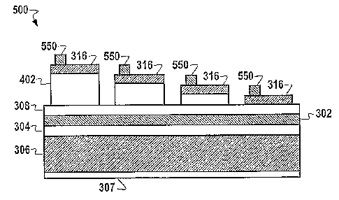
[0025] Figure 5 illustrates a side view of a VCSEL array according to the
principles of the present invention;
[0026] Figure 6 illustrates a side view of a partially fabricated VCSEL array
after a spacer is formed;
[0027] Figure 7 illustrates a side view of a partially fabricated VCSEL array
after etching the spacer of Figure 6 through binary mask set illustrated in
Figure 3;
and
[0028] Figure 8 illustrates a top view of another binary mask set that is in
accord with the principles of the present invention
[0029] Note that in the drawings that like numbers designate like elements.
Additionally, for explanatory convenience the descriptions use directional
signals
such as up and down, top and bottom, and lower and upper. Such signals, which
are
7
CA 02472061 2004-06-25
WO 03/058775 PCT/US02/41735
derived from the relative positions of the elements illustrated in the
drawings, are
meant to aid the understanding of the present invention, not to limit it.
DETAILED DESCRIPTION OF TIIE ILLUSTRATED EMBODIMENTS
[0030] The principles of the present invention provide for VCSEL arrays, and
for methods of fabricating such VCSEL arrays, that output light at multiple
wavelengths. Such VCSEL arrays are particularly useful in wavelength division
multiplexed applications.
[0031] The principles of the present invention provide for forming spacers
using a binary mask set. Binary masks have open and closed xegions that can
conceptually correspond to binary digits (Os and ls). Figure 3 illustrates one
set 200
of binary masks, with that set being comprised of a first mask 202 and of a
second
mask 204. Each mask is comprised of open areas 206 (which can correspond to
binary 0) and closed areas 208 (which can corresponds to binary 1).
[0032] A first use of the mask set 200 is in producing a special spacer using
material depositions. Turn now to Figure 4 for a partially fabricated VCSEL
structure
300. That VCSEL structure is produced by forming an active region 302 on a
lower
DBR 304, which is on a substrate 306 having a metallic contact 307. Over the
active
region is an optional top buffer layer 308. If used, the top buffer layer 308
controls the
minimum separation between the lower DBR 304 and upper DBRs that will be
formed.
[0033] The first mask 202 is placed over the partially fabricated VCSEL
structure 300 active region 302 (or over the top buffer layer 308). Spacer
material 310
having a thickness 2L is then grown (deposited) through the open areas 206 of
the
first mask. Then, the first mask 202 is removed and the second mask 204 is
placed
8
CA 02472061 2004-06-25
WO 03/058775 PCT/US02/41735
over the partially fabricated VCSEL structure 300. Spacer material 312 having
a
thickness L is then grown through the open areas 206 of the second mask. Then,
the
second mask 204 is removed. Top DBRs 316 are then grown on the deposited
spacer
layers (isolation regions, which are not shown in Figure 3, are fabricated as
required)
such that discrete VCSEL elements are produced. The result is four DBRs 316
that
are spaced apart from each other, with the thickness of each spacer element
being an
integer multiple of L.
[0034] Still referring to Figure 4, suitable spacer materials include regrowth
AlXGa~1_X~As (or similar materials), a dielectric deposition (such as PECVD
SiOz), or
a glass deposition. If the deposited spacer materials) is properly selected,
the spacer
can be relatively stress-free. Stress can further be reduced by annealing the
structure
300 after each deposition to smooth out interface roughness. Additionally,
while the
foregoing is described as producing DBR separations that are multiples of L,
this is
not required. The thickness of the various depositions can be varied to
achieve design
goals.
[0035] Referring now to Figure 5, electrical contacts 510 are then formed on
the DBRs 316. The result is a VCSEL array 500 that emits light at different
wavelengths from the individual VCSEL elements.
[0036] Another use of the mask set 200 shown in Figure 3 is in producing a
special spacer by etching. Turn now to Figure 6 for a partially fabricated
VCSEL
structure 400. That VCSEL structure is produced by forming an active region
302 on
a lower DBR 304, which is on a substrate 306 having a contact 307. Over the
active
region is an optional top buffer layer 308. If used, the top buffer layer 308
controls the
minimum separation between the lower DBR 304 and upper DBRs that will be
formed later. Over the active region is a material 402. That material can be a
dielectric
9
CA 02472061 2004-06-25
WO 03/058775 PCT/US02/41735
deposition or a semiconductor growth. Additionally, to assist accurate
etching, etch
stop layers 412 can be located within the material 402.
[0037] Referring now to Figure 7, the first mask 202 is located over the
material 402. The material 402 is then etched a distance 2L through the open
areas
206 of the first mask. An etch stop layer 412 can be used to stop the etch at
the proper
location. Then, the first mask 202 is removed and the second mask 204 is
located over
the partially fabricated VCSEL structure. The material 402 is then etched a
distance
L through the open areas 206 of the second mask. Again, an etch stop layer can
assist
accurate etch depth. Then, the second mask 204 is removed. Top DBRs 316 are
then
grown on the etched spacer layers. The result is four DBRs 316 that are spaced
apart
from each other, with the separation between each of the DBRs 316 being an
integer
multiple of L. Electrical contacts (which axe not shown, but reference the
contacts 550
in Figure 5) for the individual VCSEL elements are then provided. Isolation
regions
are also formed in suitable locations.
[0038] Referring now to Figures 6 and 7, the etch process is best performed
using an etchant that depends on the material 402. Isotropic planar etching is
beneficial. Furthermore, the material 402 can include embedded etch stop
layers 412
to enable accurate control of each step's position.
[0039] Wavelength tuned VCSEL arrays produced using binary masks have
the advantages of being able to produce a wide range of spacer thicknesses
using
lithographic techniques and relatively few masks and process steps.
Furthermore,
VCSEL arrays according to the present invention are relatively easily
fabricated using
normal fabrication processes. Also, standard processes can be used to
fabricated
features of the VCSEL array, such as trenches for oxidation and material
growths.
CA 02472061 2004-06-25
WO 03/058775 PCT/US02/41735
[0040] The foregoing has described using a binary mask set that is comprised
of two individual masks (reference Figure 3). However, the principles of the
present
invention encompass that use of other mask sets. For example, Figure 8
illustrates a
mask set 600 that is comprised of four individual masks, the masks 602, 604,
606, and
608. Those masks still include open areas 206 and closed areas 208. Such a
mask set
with 4 individual masks can produce up to 16 thickness variations. The number
of
thickness variations is related to a power of 2.
[0041] The embodiments and examples set forth herein are presented to best
explain the present invention and its practical application and to thereby
enable those
skilled in the art to make and utilize the invention. Those skilled in the
art, however,
will recognize that the foregoing description and examples have been presented
for
the purpose of illustration and example only. Other variations and
modifications of
the present invention will be apparent to those of skill in the art, and it is
the intent of
the appended claims that such variations and modifications be covered. The
description as set forth is not intended to be exhaustive or to limit the
scope of the
invention. Many modifications and variations axe possible in light of the
above
teaching without departing from the spirit and scope of the following claims.
It is
contemplated that the use of the present invention can involve components
having
different characteristics. It is intended that the scope of the present
invention be
defined by the claims appended hereto, giving full cognizance to equivalents
in all
respects.
11