Note: Descriptions are shown in the official language in which they were submitted.
CA 02473031 2004-07-09
WO 03/058816 PCT/EP03/00063
A Crossbar Device With Reduced Parasitic Capacitive Loading
and Usage of Crossbar Devices in Reconfigurable Circuits
BACKGROUND OF THE INVENTION
1. Field of the Invention
The present invention relates to the field of integrated circuit (IC). More
specifically, the present invention relates to crossbar devices, and their
usage in
reconfigurable circuits.
2. Background Information
Crossbar devices for programmatically connecting n inputs to m outputs, in
general, are known in the art.
Figures 1 a-1 b show a basic implementation of a pass n-mos crossbar device
known in the art. Input lines 100 are connectable to output lines 101 through
switches 102. Each switch 102 comprises a n-mos pass transistor 103 with its
source connected to one input line and its drain connected to one output line;
and a
memory element 104 controlling the gate of pass transistor 103. Connection
between one input line and one output line is effectuated by applying a high
voltage
(by storing a 1 in the memory element) to the gate of the corresponding pass
transistor; putting the pass transistor in a low resistance state between its
source
and drain. Output buffer 105 amplifies and regenerates the voltage level on
the
output line, restoring the pass transistor 103 threshold voltage (Vth) drop.
The
configuration of such a crossbar should connect only one input to one output,
CA 02473031 2004-07-09
WO 03/058816 PCT/EP03/00063
2
otherwise it can possibly create a short circuit between two inputs connected
to the
same output. This type of crossbar causes problems at power up if the memory
element is unknown, possibly connecting several inputs to a same output. Also,
this
type of crossbar needs n x m memory elements to realize a n inputs to m
outputs
crossbar.
Figure 2 shows another prior art implementation (US PAT 6,289,494) having
a more efficient structure. This type of crossbar needs (n / 4) x m memory
elements
201 and m 2 to 4 decoders 202 to realize a n inputs to m outputs crossbar. For
a
large crossbar input number the penalty of the 2 to 4 decoder 202 is
compensated
by the reduction in the number of memory elements required. One problem with
this
architecture is the capacitive loading of the input lines. To connect input
line 203a to
output line 204 a 1 is programmed into memory element 201a, and the decoder
drives a I on its output 205b. Therefore, input line 203b is connected to
capacitor
206. Similarly, every fourth input of one column is connected to a capacitor
206.
Note, the capacitive load of one input depends on the programming pattern of
the
other inputs, which could ends up with a high capacitive load on some input
lines
and a low capacitive load on some other input lines. Also, the capacitance 206
is
pretty big because it represents the parasitic load of five n-mos
drains/sources and
the metal interconnections between these five n-mos drains/sources.
Figure 3 shows another prior art implementation (US PAT 5.260.610). This
type of crossbar also needs (n / 2) x m memory elements 301 pfus m memory
elements 302. To connect input line 303a to output line 304 we must program a
I in
memory element 301 and a I in memory element 302. But, by programming a one
in memory element 301, input line 303b is connected to capacitance 306.
Capacitance 306 is large because it represents the parasitic load of half of
the pass
transistor of one column plus the metal interconnection between them. If the
CA 02473031 2004-07-09
WO 03/058816 PCT/EP03/00063
3
crossbar has 32 inputs, then capacitance 306 includes the parasitic load of 16
n-
mos drains/sources. Again, the capacitive loading of one input lines can vary
dramatically with the programming pattern of the other inputs.
In application where a significant number of crossbar are employed and
interconnected, such as reconfigurable circuit applications, the input
capacitive load
variation of one crossbar input with respect to the programming pattern of its
other
inputs makes the timing optimization of high performance devices very
difficult.
Additionally, these and other prior art crossbar devices are found to consume
more
power and/or area than desired, as well as contributing to current swing.
Thus, a crossbar device and techniques of employment in reconfigurable
circuit without at least some of these disadvantages are desired.
CA 02473031 2004-07-09
WO 03/058816 PCT/EP03/00063
4
SUMMARY OF THE INVENTION
A crossbar device includes a first set of input conductor lines and a second
set of output conductor lines. A plurality of chains of pass transistors are
provided to
selectively couple the input lines to the output lines in a reduced parasitic
capacitive
loading manner. Further, memory elements and decoder logic are provided to
facilitate control of the selective coupling.
In one embodiment, each pass transistor chain comprises a first pass
transistor with its source connected to one input line and its gate connected
to a
memory element, and a second pass transistor with its source connected to the
drain of the first pass transistor, its gate connected to a decoder logic, and
its drain
connected to one output line. For each output line, the memory element selects
a
first group of inputs and the decoder selects one input out of the first group
of inputs
thereby establishing a connection between the selected input line and the
output
line.
In accordance with another aspect, a low power application of multiple
crossbar devices to a reconfigurable circuit block is improved by having each
memory element of a crossbar device be provided with a supply voltage higher
by a
threshold voltage Vth to maintain the supply voltage of corresponding output
buffers
input at Vdd, to prevent the output buffers from consuming static current when
their
inputs are at a degenrated level, to facilitate the lower power application.
In accordance with yet another aspect, an application of multiple crossbar
devices to a reconfigurable circuit block is improved by coupling a control
circuitry
via a control line to all output buffers of the interconnected crossbar
devices to force
all output buffers of the crossbar devices to a known state at power-on, to
prevent
unpredictable behavior.
CA 02473031 2005-06-17
4a
In a further aspect, the present invention provides a crossbar device
comprising: n input lines; m output lines; and a plurality of chains of pass
transistors, each having a plurality of pass transistors, to selectively
couple said
n input lines to said m output lines; where n and m are integers.
In a still further aspect, the present invention provides a reconfigurable
circuit comprising: a plurality of crossbar devices coupled to one another,
each
crossbar device having at least a memory element, and an output buffer
electrically associated with the memory element; and a voltage supply
structure
coupled to the crossbar device designed to supply Vdd to the output buffers,
and
a voltage raised by a threshold over Vdd to the memory elements to maintain
the
input voltage of the output buffers at Vdd.
In a further aspect, the present invention provides a reconfigurable circuit
comprising: a plurality of crossbar devices coupled to one another, each
crossbar device having at least an output buffer; and a power-on circuitry
coupled to the crossbar devices to force the output buffers to a known state
at
power-on.
In a still further aspect, the present invention provides a crossbar device
comprising: n input lines; m output lines; and a plurality of chains of pass
transistors, each chain having a plurality of pass transistors, to selectively
couple
said n input lines to said m output lines, wherein each of the plurality of
chains of
pass transistors comprises a first and a second pass transistors coupled such
that said first pass transistor drives a load consisting essentially of said
second
pass transistors and interconnect between said first and said second pass
transistor; where n and m are integers.
In a further aspect, the present invention provides a reconfigurable circuit
comprising: a plurality of crossbar devices coupled to one another, each
crossbar device having at least a memory element, and an output buffer
electrically associated with said at least a memory element; and a voltage
supply
structure coupled to at least one crossbar device designed to supply Vdd to an
input to the output buffer and to raise a voltage raised by a threshold over
Vdd to
CA 02473031 2009-03-02
4b
said at least a memory element to maintain an input voltage of the output
buffer
at Vdd.
In a still further aspect, the present invention provides a reconfigurable
circuit comprising: a plurality of crossbar devices coupled to one another,
each
crossbar device having at least an output buffer; and a power-on circuitry
coupled to the crossbar devices to force the output buffers to a same known
logic value at power-on, said same known logic value to facilitate reduction
of
current drain in said reconfigurable circuit by reducing the number of outputs
of
said plurality of output buffers at different logic values.
In a further aspect, the present invention provides a crossbar device
comprising: n input lines; m output lines; and a plurality of chains of pass
transistors, each chain having a plurality of pass transistors, to selectively
couple said n input lines to said m output lines, wherein each of the
plurality of
chains of pass transistors comprises a first and a second pass transistor
coupled such that said first pass transistor drives a load consisting
essentially
of said second pass transistor and interconnect between said first and said
second pass transistor, and wherein a gate of the first pass transistor is
coupled to a first signal and a gate of the second pass transistor is coupled
to a
second signal; where n and m are integers.
CA 02473031 2004-07-09
WO 03/058816 PCT/EP03/00063
BRIEF DESCRIPTION OF DRAWINGS
The present invention will be described by way of exemplary embodiments,
but not limitations, illustrated in the accompanying drawings in which like
references
5 denote similar elements, and in which:
Figures 1a-1b illustrate a basic crossbar implementation known in the art;
Figures 2-3 illustrate additional prior art implementations;
Figure 4 illustrates the improved crossbar device of the present invention, in
accordance with one embodiment;
Figure 5 illustrates the dual pass transistor layout, in accordance with one
embodiment;
Figure 6 illustrates a low power application of crossbar devices in a
reconfigurable circuit, in accordance with one embodiment; and
Figure 7 illustrates a technique to improve employment of a large number of
crossbar devices in a reconfigurable circuit, in accordance with one
embodiment.
CA 02473031 2004-07-09
WO 03/058816 PCT/EP03/00063
6
DETAILED DESCRIPTION OF THE INVENTION
In the following description, for purposes of explanation, specific numbers,
materials and configurations are set forth in order to provide a thorough
understanding of the present invention. However, it will be apparent to one
skilled in
the art that the present invention may be practiced without the specific
details. In
other instances, well-known features are omitted or simplified in order not to
obscure
the present invention.
Further, the phrase "in one embodiment" is used repeatedly. In general, the
phrase does not refer to the same embodiment, although it may. The terms
"comprising", "including", "having" and the like, as used in the present
application, are
synonymous.
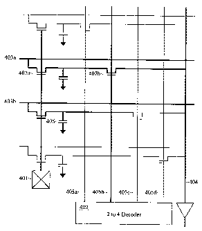
Referring now to Figures 4-5, wherein the crossbar device of the present
invention, in accordance with one embodiment is shown. The crossbar device
includes (n / 4) x m memory elements 401 plus m 2 to 4 decoders 402 for
selectively
control the coupling of n inputs to m outputs. As illustrated, the crossbar
device
advantageously uses a dual gate pass transistor structure to minimize the
parasitic
capacitive loading of the input lines. Each input line, e.g. input line 403a
is
connected to a output line, such as output line 404, by way of a chain of pass
transistors, such as pass transistors 407a and 407b.
To connect input line 403a to output line 404, a 1 is programmed in memory
element 401 and the decoder 402 drives a 1 on line 405b. By programming a 1 in
memory element 401 input line 403b is connected to capacitance 406. However,
as
a result of the dual gate pass transistor structure, parasitic capacitance 406
is
reduced to a small active area as depicted on Figure 5. Therefore, although
the
CA 02473031 2004-07-09
WO 03/058816 PCT/EP03/00063
7
input line parasitic load caused by the programming pattern of the other input
lines
is not totally suppressed, the present invention substantially reduces it to
the layout
of the drain/source area while employing a small number of memory elements to
realize the crossbar device.
While for ease of understanding, Fig. 4 illustrated the chain of pass
transistors coupling an input line to an output line as having two pass
transistors, in
alternate embodiments, the present invention may be practiced with the chain
as
having more than two pass transistors with the first pass transistor,
connected to the
input line, controlled by a local memory element like 401 and the other pass
transistor of the chain controlled by a decoder circuitry or memory elements.
In low power applications where a number of crossbar devices are
interconnected, it is important to reduce the voltage swing on the
interconnections
between the crossbar devices, to reduce the dynamic current. Figure 6 shows a
low power structure suitable for use in a crossbar device, in accordance with
another aspect of the present invention. The lower power attribute is achieved
by
lowering the supply voltage 601 of the crossbar output buffer 603 and the
additional
drivers providing inputs to the various crossbar of the circuit. When a VDD
level is
applied on input line 606, output line 607 receives a degenerated level VDD -
threshold voltage Vth, because of the Vth drop across n-mos pass transistors
602.
This degenerated level when applied on the input of crossbar output buffer 603
produces a parasitic current flowing through the first inverter stage. This
parasitic
current, when multiplied by a significant number of crossbar output buffers of
an
integrated circuit block, such as a FPGA block, may ruin the low power target.
As
illustrated in Figure 6, the Vth drop is advantageously compensated by raising
supply voltage 605 for memory element 604 by Vth. As a result, the gate of the
pass
. i . , . . . . . . . . . . . . . .. .. . . .
CA 02473031 2009-03-02
8
transistor 602 receives a voltage level that is one Vth above the voltage
level of
input line 606. However, this voltage raise does not impact the circuit power
because there is no static or dynamic current in the memory element during the
circuit operation. Resultantly, the crossbar output line transistor 602
receives a
voltage level that is one Vth above the voltage level of input line 606.
However,
this voltage raise does not impact the circuit power because there is no
static or
dynamic current in the memory element during the I circuit operation.
Resultantly, the crossbar output line 607 has a full VDD level.
The crossbar device may be the crossbar device of the present invention
as illustrated in Fig 4-5. Alternatively, the crossbar device may also be a
crossbar device of the prior art having the requisite memory and output buffer
elements.
As alluded to earlier, employing crossbar devices in a low power manner
is especially desirable for an integrated circuit or integrated circuit block
where
a significant number of crossbar devices are employed and interconnected. An
example of such integrated circuit is the scalable reconfigurable circuit
disclosed in U.S. Patent No. 6,594,810 entitled "Reconfigurable Integrated
Circuit with a Scalable Architecture", issued July 15, 2003, having common
inventorship with present application.
The present invention contemplates IP blocks incorporated with the
teachings of the present invention for incorporation into reconfigurable
integrated circuits, as well as integrated circuits directly practicing the
teachings
of the present invention.
Figure 7 shows an improved crossbar output buffer structure to
avoid static I current at power-up, in accordance with yet another aspect of
the present invention. As mentioned above, at power-up, the state of the
memory elements are undefined. This may create various paths between
the inputs of a crossbar. For a reconfigurable circuit block, such as the one
disclosed in copending application '123, many output buffers may be
shorted together at power-up, producing a large current flow through the
device. Also, during configuration loading sequence of the circuit
CA 02473031 2004-07-09
WO 03/058816 PCT/EP03/00063
9
block, the incomplete configuration may temporary create short circuits
between the
crossbar inputs. To compensate for these possibilities, the output buffers 704
are
advantageously connected to a global control line 701 forcing their outputs to
a
known level. This control line is activated by a power-on reset circuitry 702
and is
desactivated when a configuration has been loaded in the reconfigurable
circuit
block. Since all the crossbar outputs are at the same level during the power-
up and
until a configuration is loaded, the fact that they may or may not be shorted
together
does not produce any more current. For example, at power up, power on reset
circuitry 702 resets the flip-flop 703. The flip-flop output 701 forces all
the crossbar
buffers 704 to zero. When a configuration is loaded, flip flop 702 is written
with a
logical 1, enabling all crossbar output buffers.
The crossbar device may be the crossbar device of the present invention as
illustrated in Fig 4-5. Alternatively, the crossbar device may also be a
crossbar
device of the prior art having the requisite memory and output buffer
elements.
Further, the technique disclosed in Fig. 7 may also be practiced in
conjunction with
the voltage supply technique of Fig. 6.
As alluded to earlier, the present invention contemplates IP blocks
incorporated with the teachings of the present invention for incorporation
into
reconfigurable integrated circuits, as well as integrated circuits directly
practicing the
teachings of the present invention.
Thus an improved crossbar device with reduced parasitic capacitive loading,
and improved techniques for using a significant number of crossbar devices
have
been disclosed. As alluded to earlier, the described embodiments are
illustrative,
and not restrictive. The present invention may be practiced with modifications
and
CA 02473031 2004-07-09
WO 03/058816 PCT/EP03/00063
alterations to the described embodiments, consistent with the scope of the
invention
as set forth by the claims below.