Note: Descriptions are shown in the official language in which they were submitted.
CA 02473396 2004-07-13
WO 03/063305 PCT/US03/01413
HIGH COHERENT POWER, TWO-DIMENSIONAL SURFACE
EMITTING SEMICONDUCTOR DIODE ARRAY LASER
FIELD OF THE INVENTION
[0001 ] This invention pertains generally to the field of
semiconductor diode lasers and diode laser arrays.
BACKGROUND OF THE INVENTION
[0002] Phase locked arrays of antiguide laser structures were
demonstrated over a decade ago. See, D. Botez, et al. "High-Power
Diffraction Limited Beam Operation from Phase Locked Diode Laser Arrays
of Closely Spaced 'Leaky' Wave Guides (Antiguides)," Appl. Phys. Lett.,
Vol. 53, 1988, pp. 464 et seq. In an antiguide laser, the antiguide core
has an index no lower than the cladding index, n,. Whereas in a positive
index guide, light is trapped in the guide core via total internal reflection,
in an antiguide light is only partially reflected at the antiguide-core
boundaries. Light refracted into the cladding layers is radiation leaking
outwardly with lateral (projected) wavelength ~,,, and can be thought of
as a radiation loss, a~. See, D. Botez, "Monolithic Phase-Locked
Semiconductor Laser Arrays," Chapter 1 in Diode Laser Arrays, D. Botez
and D.R. Scifres, Eds. Cambridge, U.IC., Cambridge Univ. Press, 1994,
pp. 1-72. For a proper mode to exist, ar has to be compensated for by
gain in the antiguide core. The effective indices of the supported leaky
modes have values below the core index, the quantum-mechanical
equivalent being quasi-bound states above a potential barrier. Although in
a single antiguide the radiation losses can be quite high, closely spacing
antiguides in linear arrays significantly reduces the device losses, since
-1-
CA 02473396 2004-07-13
WO 03/063305 PCT/US03/01413
radiation leakage from individual elements mainly serves the purpose of
coupling the array elements.
[0003] Due to lateral radiation, a single antiguide, for which the
index of refraction varies in only one dimension, can be thought of as a
generator of laterally propagating traveling waves of wavelength ~,,. In an
array of antiguides, elements will resonantly couple in-phase or out-of-
phase when the interelement spacings correspond to an odd or even
number of (lateral) half-wavelengths ~,,/2, respectively. When the
resonance condition is met, the interelement spacings become Fabry-Perot
resonators in the resonance condition, and thus full transmission occurs
through the array structure allowing each element to equally couple to all
others (i.e., global coupling is achieved). Resonant leaky-wave coupling
allows the realization of global coupling for any type of phase locked laser
array. See, D. Botez, et al. "Resonant Leaky-Wave Coupling in Linear
Arrays of Antiguides," Electron. Lett., Vol. 24, August 1988, pp. 1328-
1330; D. Botez, et al. "Resonant Optical Transmission and Coupling in
Phase-Locked Diode Laser Arrays of Antiguides: The Resonant Optical
Waveguide Array," Appl. Phys. Lett., Vol. 54, May 1989, pp. 2183-
2185. At its resonance, the in-phase mode intensity profile becomes
uniform. The unwanted out-of-phase models) are non-resonant, which
causes their fields to be significantly trapped between elements, and
these modes can thus be effectively suppressed using interelement loss.
Another way of suppressing out-of-phase modes is by the use of
intracavity Talbot-type spatial filters. See, D. Botez, et al., "Phase-Locked
Arrays of Antiguides: Modal Content and Discrimination," IEEE J.
Quantum Electron., Vol. 26, March 1990, pp. 482-485. However, the
above description for resonant leaky-wave coupling holds only for
_2_
CA 02473396 2004-07-13
WO 03/063305 PCT/US03/01413
structures in which the index of refraction varies periodically in only one
dimension, the lateral one. For real antiguided devices, the index of
refraction varies periodically in two dimensions, such that resonant
coupling of the elements does not necessarily occur when the
interelement spacings correspond to an odd or even number of (lateral)
half-wavelengths ~,,/2, respectively, but rather when the interelement
spacings correspond to an odd or even number of (lateral) half-
wavelengths 7~~/2 plus a length which is a function of the two-dimensional
details of the structure. See, D. Botez, "Monolithic phase-locked
semiconductor laser arrays," pp. 1-71 in "Diode Laser Arrays," D. Botez
and D.R. Scifres eds., Cambridge Univ. Press, UIC, 1994.
[00047 Edge emitting devices, called ROW arrays, have exceeded
the one watt coherent-power barrier (D. Botez, et al., "Watt-Range,
Coherent Uniphase Power from Phase-Locked Arrays of Antiguide Diode
Lasers," Appl. Phys. Lett., Vol. 58, May 1991, pp. 2070-2072),
demonstrated 10W of peak pulse power in a beam twice the diffraction
limit (H. Yang, et al., "1 OW Near-Diffraction-Limited Pulsed Power From
0.98 ~,m-Emitting, AI-Free Phase Locked Antiguided Arrays," Electron.
Lett., Vol. 33, 1997, pp. 136-138), and 1.6W continuous wave (CW)
power in a twice diffraction limited beam (H. Yang, et al., "1.6W
Continuous-Wave Coherent Power From Large-Index-Step [0n 0 .1 ] Near-
Resonant Antiguided Diode Laser Arrays" Appl. Phys. Lett., Vol. 76,
2000, pp. 1219-1221 ). These milestones in stable, coherent power were
due both to global coupling as well as to high built-in index steps
(On=0.05-0.10) structures, which makes the desired in-phase mode
relatively insensitive~to gain spatial hole burning (GSHB) and thermal
tensing. Comprehensive above-threshold analyses have confirmed the
-3-
CA 02473396 2004-07-13
WO 03/063305 PCT/US03/01413
basic immunity of ROW arrays to GSHB. Furthermore, unlike evanescent-
wave-coupled arrays, ROW arrays do not display coupling-induced
instabilities, as expected for globally-coupled arrays. ROW arrays, due to
large index steps as well as reliance on periodic gain modulation for
selecting lasing of specific traveling-wave modes, were effectively the
first active photonic lattices (APLs) employed for the generation of high
coherent power. Bloch-function analysis showed them to be equivalent to
2nd order complex-coupled lateral distributed feedback (DFB) structures of
zero stopgap, and further Bloch-function analyses of finite structures have
allowed the derivation of analytical formulae for all relevant design
parameters.
[0005] Antiguided-array structures have also been used for
creating other APL-type devices. These include flat phasefront, stable
beam fanout MOPA devices (See, Zmudzinski, et al., "3-Core ARROW-
Type Diode Laser: Novel High-Power Single-Mode Device, and Effective
Master Oscillator for Flared Antiguided MOPAs," IEEE J. Select. Topics
Quantum Electron., Vol. 1, No. 2, June 1995, pp. 129-137; D. Botez, et
al., "Flat Phasefront Fanout-Type Power Amplifier Employing Resonant-
Optical Waveguide Structures," Appl. Phys. Lett., Vol. 63, December
1993, pp. 3113-31 15), ARROW devices (L.J. Mawst, et al., "Design
Optimization of ARROW-Type Diode Lasers," IEEE Photonics Tech. Lett.,
Vol. 4, Nov. 1992, pp. 1204-1206; L.J. Mawst, et al., "High-Powered,
Single Mode, AI Free InGaAs, [P]/InGaP/GaAs Distributed Feedback Diode
Lasers," Journal of Crystal Growth, Vol. 195, 1998, pp. 609 et seq.; D.
Zhou, et al., "Simplified Antiresonant Reflecting Optical Wave Guide-Type
Vertical-Cavity Surface-Emitting Lasers," Appl. Phys. Lett., Vol. 76,
2000, pp. 1659 et seq.); and Triple-Core ARROW Devices (A.
-4-
CA 02473396 2004-07-13
WO 03/063305 PCT/US03/01413
Bhattacharya, et al., "0.4W CW Diffraction-Limited-Beam AI-Free,
0.98 ~,m Three Core ARROW-Type Diode Lasers," Electron. Lett., Vol. 32,
1996, pp. 657-658) which have demonstrated high CW (>_0.4W) coherent
powers, as well as well as one-dimensional and two-dimensional ROW
arrays of vertical cavity surface emitting lasers (VCSELs) (S.K. Serkland,
et al., "Two-Element Phased Array of Antiguided Vertical-Cavity Lasers,"
Appl. Phys. Lett., Vol. 75, 1999, pp. 3754 et seq.; D. Zhou, et al., "Two-
Dimensional Phase-Locked Antiguided Vertical Cavity Surface-Emitting
Laser Arrays," Appl. Phys. Lett., Vol. 77, 2000, pp. 2307 et seq.).
However, ROW arrays can be prone to self-pulsations either if saturable
absorption occurs in lossy interelement regions or when imaging, in
intracavity Talbot-type spatial filters, is disturbed by GSHB. Single-
frequency pulsed operation can be achieved for edge-emitting devices by
using DFB gratings, but the yield of in-phase-mode operating devices has
been quite low, since the effective yield is a strong function of the grating
phases) with respect to the cleaved mirror facet(s). M.P. Nesnidal, et al.,
"Distributed Feedback Grating Used as an Array-Mode Selector in
Resonant Antiguided Diode Laser Arrays: Effects of the Mirror Facet
Position With Respect to the Grating," IEEE Photon. Tech. Lett., Vol. 10,
1998, pp. 507 et seq.; and N. Nesnidal, et al., "0.45 W Diffraction-
Limited-Beam and Single-Frequency Operation from Resonant Antiguided
Phase-Locked Laser Array With Distributed Feedback Gratings," Appl.
Phys. Lett., Vol. 73, 1998, pp. 587 et seq.
[0006] Second-order DFB laser structures for use as surface
emitters, based on outcoupling perpendicular to the chip surface, have
been studied for nearly three decades. However, it has been found both
theoretically as well as experimentally that the favored mode to lase is an
-5-
CA 02473396 2004-07-13
WO 03/063305 PCT/US03/01413
antisymmetric one (that is, a two-lobed pattern), since it has the least
radiation loss. Furthermore, the guided-field pattern is highly nonuniform,
making the device vulnerable to multimoding via longitudinal GSHB. C.H.
Henry, et al., "Observation of Destructive Interference in the Radiation
Loss of Second-Order Distributed Feedback Lasers," IEEE J. QE, Vol. 21,
1985, pp. 151-153.
[0007] Several approaches have been tried to obtain symmetric-
like mode operation or actual symmetric mode operation. The first
approach involves using a ~ phase-shifting film deposited on half the
device aperture (S.H. Macomber, et al., "Recent Developments in Surface
Emitting Distributed Feedback Arrays," Proc. SPIE, Vol. 1219, 1990, pp.
228 et seq.), an impractical method, which does not solve the guided-
field nonuniformity issue, or a long (about 2 mm) chirped grating (S.H.
Macomber, "Nonlinear Analysis of Surface-Emitting Distributed Feedback
Lasers," IEEE J. QE, Vol. 26, 1990, pp. 2065-2074), which phase shifts
the antisymmetric mode such that the devices operate in an off-normal
single lobe pattern. The second of the approaches causes pure
symmetric-mode operation either by preferential carrier injection in a
weak-coupling grating region (N.W. Carlson, "Mode Discrimination in
Distributed Feedback Grating Surface Emitting Lasers Containing a Buried
Second Order Grating," IEEE J. QE, Vol. 27, 1991, pp. 1746-1752), or by
introducing a metal grating which suppresses antisymmetric-mode lasing
(M. Kasraian, et al., "Metal Grating Outcoupled, Surface-Emitting
Distributed Feedback Diode Lasers," Appl. Phys. Lett., Vol. 69, 1996, pp.
2795-2797). However, preferential carrier injection is not a long-term
reliable approach, and the scheme, due to the necessity for weak coupling
grating, inherently leads to inefficient devices (about 10% efficiency).
-6-
CA 02473396 2004-07-13
WO 03/063305 PCT/US03/01413
The metal grating approach is feasible but introduces too much of a
penalty loss for the symmetric mode, such that efficiencies are at best
25-30%, and the gain thresholds are quite high (about 70 cm-').
[0008] More recently, a solution to obtaining a symmetric-mode
beam pattern with no penalty in device efficiency has been found in the
use of central grating phase shifts of around ~ in distributed
feedback/distributed Bragg reflector (DFB/DBR) devices. G. Witjaksono,
et al., "Surface-Emitting Single Lobe Operation from 2"d-Order Distributed-
Reflector Lasers With Central Grating Phase Shift," Appl. Phys. Lett., Vol.
78, 2001, pp. 4088-4090; Dan Botez, et al., "Single Mode, Single Lobe
Surface Emitting Distributed Feedback Semiconductor Laser," Published
International Application No. WO 01 /13480 A1, 22 February 2001. An
example is a structure having a double-quantum-well (DQW)
InGaAs/InGaAsP active region with InGaP cladding layers, and a grating
formed in a P+-GaAs cap layer. The DQW active region is designed to be
0.4-0.5 ~,m away from the metal contact such that the device efficiency
and reliability are unaffected. A symmetric-like mode is favored to lase
over the antisymmetric-like mode when the grating phase shift, 0~, ranges
from 100° to 280°, with maximum discrimination occurring when
0~=180°, i.e., a half wave (7~/2) central phase shift. The 180°
phase
shift does not affect the in-plane propagating (guided) light, as the field
round trip through the phase shifter is 360° (i.e., the guided field
remains
antisymmetric). For the same reason, the 180° phase shift region does
not affect the DFB/DBR grating, since the lasing occurs at the same
wavelength, close to the Bragg wavelength, with or without a 180° phase
shift. That is, the 180° phase shift creates no defect in the active
photonic lattice. However, for the grating-outcoupled light, the 180°
_7_
CA 02473396 2004-07-13
WO 03/063305 PCT/US03/01413
central phase shift region defines two surface emitting regions whose
outcoupled fields are out-of-phase with each other, and thus the
outcoupling of the guided antisymmetric field provides in-phase (i.e.,
symmetric) radiated near-field and far-field patterns. These types of
devices also allow for relatively large tolerances in device fabrication,
providing a practical solution for single (orthonormal)-lobe efficient surface
emission from 2"d-order DFB lasers.
[0009] For devices optimized for maximum external differential
quantum efficiency, rld, the variation of the threshold gain and rld have
been studied as a function of the grating duty cycle, 6, defined as the
ratio of Au as part of the grating period. G. Witjaksono, et al., "High-
Efficiency, Single-Lobe Surface Emitting DFB/DBR Lasers," Paper TuA3,
14t" IEEE LEOS. Annual Meeting, 12-15 Nov. 2001, San Diego, CA. The
intermodal discrimination, Da, reaches a maximum 1 13 cm-' for 6=0.5,
while the symmetric mode (S-mode) threshold gain is only 22 cm-' for
6=0.4, with a respectable ~a value of 52 cm-'. In general, it is found
that such devices can tolerate some variation in grating duty cycle at a
relatively small penalty in slope efficiency.
[0010] Gratings with phase shifts can be patterned by e-beam
lithography or by holographic exposure of side-by-side negative and
positive resists. However, current e-beam lithography allows writing of
gratings only 400-600 ~,m long, and for devices requiring relatively long
gratings (e.g., about 1,500 p,m), fabrication by e-beam lithography is not
advisable. The holographic method has been used to fabricate 1 St-order
gratings with quarter-wave (i.e., ~/2) phase shifts, with the transition
from negative to positive resists creating a grating phase shift of half the
grating period. Using the same method for 2"d-order gratings naturally
_g_
CA 02473396 2004-07-13
WO 03/063305 PCT/US03/01413
provides half-wave (i.e., ~) phase shifts. Semiconductor (GaAs) gratings
with ~ phase shifts have been developed using negative and positive
resists (G. Witjaksono, et al. paper, TuA3, supra). A transition region is
observed, but its width is not that relevant as long as the two grating
regions are out of phase with each other. That is, the grating phase shift
does not necessarily have to be ~; it can be an odd number of ~, since the
in-plane propagating (guided) light is unaffected by it.
[0011 ] Two-dimensional (2-D) single-mode, single-lobe surface
emitters (horizontal resonant cavity) are ideal high-power (>_1 W) coherent
sources due both to low aspect ratio beams as well as the potential for
scaling up the power by the use of coherent coupling of the sources at
the wafer level (i.e., monolithically). L.J. Mawst, et al., "2-D Coherent
Surface-Emitting Leaky Wave Coupled Laser Arrays," IEEE J. Quantum
Electron, Vol. 29, 1993, pp. 1906-1917. Three such types of devices
have been reported. One involves angled gratings, K.N. Dzurko, et al.,
"Distributed Bragg Reflector Ring Oscillators: Large Aperture Source of
High Single Mode Optical Power," IEEE J. Quantum Electron., Vol. 29,
1993, pp. 1895-1899; M. Fallahi, et al., "Low Threshold CW Operation of
Circular-Grating Surface-Emitting DBR Lasers Using MQW and a Self-
Aligned Process," IEEE Photon. Tech. Lett., Vol. 6, 1994, pp. 1280-
1282. The third approach uses a curved-grating unstable resonator, S.H.
Macomber, et al., "Curved-Grating Surface-Emitting DFB Lasers and
Arrays," Proceedings Society of Photo-Optical Instrumentation Engineers,"
Vol. 3001, 1997, pp. 42-54. However, none of these devices have a
built-in dielectric structure for lateral-optical-mode control and stability,
and as a result are vulnerable to temperature and carrier induced
dielectric-constant variations. An example of such behavior is the
_g_
CA 02473396 2004-07-13
WO 03/063305 PCT/US03/01413
unstable resonator device which, while operating single-mode to high
peak pulsed power in a single off-normal beam, readily becomes
multimode in CW operation due to thermal tensing.
SUMMARY OF THE INVENTION
[0012] The semiconductor diode array lasers of the present
invention utilize periodic dielectric structures with modulated optical gain,
so-called active photonic lattices (APLs), to realize watt-range coherent,
surface-emitted powers from 2-dimensional (2-D) horizontal cavity devices
with 2"d order gratings of novel design. In contrast to conventional APLs,
the devices in accordance with the invention have gain in the low-index
lattice sites, enabling long range (coherent) coupling by traveling waves
utilizing resonant leaky-wave coupling between the low-index lattice sites,
which had previously only been possible for 1-dimensional edge-emitting
structures (so-called antiguided array structures).
[0013] The antiguided array structures of the present invention
for the lateral dimension preferably have large index steps (e.g., ~n~0.10),
which ensure optical-mode stability against carrier and thermal induced
dielectric-constant variations. The 2-D devices of the present invention
combine antiguided phase locked arrays with surface emission from 2"d-
order DFB/DBR grating structures. Unlike prior 2-D order grating DFB
surface emitters, the present invention utilizes central grating phase shifts
of around 180°, which provides emission in an orthonormal, single lobe
beam at no penalty in device efficiency. The grating structure, as well as
ensuring single longitudinal-mode operation, acts as a highly efficient
selector of a single lateral mode, the in phase array mode. As a
consequence, large aperture (e.g., 200 p,m x 1200 Vim) coherent laser
-10-
CA 02473396 2004-07-13
WO 03/063305 PCT/US03/01413
diode sources in accordance with the invention have nearly uniform 2-D
guided-field profiles and thus are able to operate in a stable, single
diffraction-limited beam to watt-range CW output powers. Beam
circularization can then be readily obtained utilizing commercially available
optical components.
[0014.] The present invention enables CW watt-range, stable,
single mode laser light sources that may be utilized for applications such
as room-temperature CW mid-IR (7~=3-5 p.m) coherent light generation
(via frequency up-conversion) that can provide several orders of
magnitude increases in the sensitivity of laser-absorption spectroscopy for
a wide array of non-invasive medical diagnostics (e.g., breath analysis),
and for IR countermeasures; for the generation of hundreds of mWs of
blue light via harmonic conversion for applications such as in
biotechnology (e.g., flow cytometry) and for laser projection systems; for
high-power low-noise, high-fidelity RF optical links; and for coherent free-
space optical communications. The devices of the present invention are
single frequency and thus ideally suited for scalability at the wafer level
(via resonant leaky-wave coupling) to 20 units or more. This enables all-
monolithic laser light sources capable of providing tens of watts of
coherent, uniphase power for various applications, such as high-
efficiency, high resolution magnetic resonance imaging with noble gases.
(0015] The surface-emitting devices of the present invention
have the advantages over edge-emitting devices for the generation of high
(greater than 1 W) CW coherent powers that: complete passivation of the
emitting area is not needed for reliable operation, scalability at the wafer
level becomes possible, and packaging is significantly simplified.
-1 1-
CA 02473396 2004-07-13
WO 03/063305 PCT/US03/01413
[0016] The semiconductor diodes of the present invention
preferably utilize gain in the low-index lattice sites, which in turn allows
long range coherent coupling via traveling waves. The use of a ~c phase
shifter centrally located in a second order grating serves to provide single-
lobe, orthonormal beam emission with high efficiency (greater than 60%),
and the use of gratings with dual spatial-mode selectivity provides both
conventional longitudinal-mode selection and strong lateral-mode selection
for phase-locked antiguided arrays. In the lateral direction, spatial
coherence is obtained by using a phase-locked antiguided array, which
corresponds to a 1-dimensional edge emitting active photonic lattice, and
using traveling waves for element coupling. The coupling is resonant and
long-range by having the high-index regions correspond to an integral
number of lateral half waves, thus making the structure fully transmissive.
Although the index step may be relatively small compared to those
commonly used in photonic lattices, photonic bands and band gaps are
formed. Such devices are in effect lateral 2"d-order complex coupled DFB
structures whose 2"d diffraction order provides lateral coupling while the
1 St diffraction order provides propagation in a direction parallel to the
array
elements and edge emission for edge emitting devices. At lateral
resonances, the second order Bragg condition is exactly satisfied, and the
stopgaps disappear, i.e., at resonance, full transmission across the
photonic lattice is allowed, effectively making such devices photonic band
pass devices. At resonance, antiguided arrays become pure gain-coupled
DFBs, which are well known to have no stopgaps and thus will lase at the
Bragg frequency.
[0017] In the longitudinal direction, coherence is obtained by
using a 2"d-order grating with a DFB region for gain, partial feedback and
-12-
CA 02473396 2004-07-13
WO 03/063305 PCT/US03/01413
outcoupling, and DBR regions for strong frequency-selective feedback,
effectively providing a second order photonic band gap structure with a
DFB light out-coupling region. Unlike microcavity PBG structures with
built-in lattice defect (defect lasers), the photonic band gap structure in
the present invention does not have lattice defects, thus allowing for full
transmission of light over large distances and thus permitting the
generation and surface emission of high coherent power from large
apertures. Thus, the present invention combines 2"d-order photonic
lattices in both the lateral (PBP structure) and the longitudinal (PBG
structure) directions. The two lattices are interconnected in that the
longitudinally-placed grating acts as a highly effective selector of the
desired traveling-wave mode in the lateral direction -- the in-phase array
mode, i.e., mode (O,1).
[0018] Further objects, features and advantages of the invention
will be apparent from the following detailed description when taken in
conjunction with the accompanying drawings.
BRIEF DESCRIPTION OF THE DRAWINGS
[0019] In the drawings:
[0020] Fig. 1 is a simplified perspective view of a surface-
emitting DFBIDBR device operating in a single, orthonormal beam that
may be utilized as an array element in the semiconductor diode laser of
the present invention.
[0021] Fig. 2 is a schematic cross-sectional view of an
exemplary semiconductor laser element of the type shown in Fig. 1 that
has a sinusoidal-shaped grating.
-13-
CA 02473396 2004-07-13
WO 03/063305 PCT/US03/01413
[0022] Fig. 3 is a computed graph of the mode discrimination for
the device of Fig. 2 as a function of the central phase shift value, 0~.
[0023] Fig. 4 is a computed graph for the device of Fig. 2 with
~~=180° showing the near-field profile in the solid curve and the
guided-
field profile in the dashed curve.
[0024] Fig. 5 is a computed graph illustrating the far-field pattern
for the device of Figs. 2 and 4.
(0025] Fig. 6 are computed graphs for the device of Figs. 2 and
4 showing the differential quantum efficiency, rid, and the effective rld.
[0026] Fig. 7 is a computed graph for the device of Figs. 2 and 4
illustrating the guided-field peak-to-valley ratio R' in the active (i.e.,
DFB)
region as a function of the phase shift 0~.
[0027] Fig. 8 is a simplified perspective view of an antiguided
diode array laser in accordance with the invention having a central phase
shift DFB/DBR grating structure.
(0028] Fig. 9 is a perspective view of the device of Fig. 8
illustrating emission from the surface of the substrate of the device.
(0029] Fig. 10 is an illustrative cross-sectional view of the device
of Fig. 9 taken generally along the lines 10-10 in Fig. 9.
(0030] Fig. 1 1 is a graph illustrating the transverse field-intensity
profile in the array element regions (ne~~=3.28) of the device of Figs. 8
and 9.
-14-
CA 02473396 2004-07-13
WO 03/063305 PCT/US03/01413
[0031 ] Fig. 12 is a graph illustrating the transverse field-intensity
profile in the interelement regions (nef~=3.34) in the device of Figs. 8 and
9.
[0032] Fig. 13 is a graph illustrating the near-field intensity
profile of the upper adjacent array mode of a 10-element ROW array.
[0033] Fig. 14 is a plan view of a laser diode array structure in
accordance with the invention that is arranged for suppressing oscillation
of the upper-adjacent mode of 40-element ROW arrays.
[0034] Fig. 15 is a simplified plan view of a scaled array device
in accordance with the invention in which individual devices are coupled
in the array.
[0035] Fig. 16 is an array as in Fig. 15 having 16 laser diode
array units.
[0036] Fig. 17 is a simplified cross-sectional view through the
interdevice regions of the array of Fig. 16.
DETAILED DESCRIPTION OF THE INVENTION
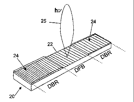
[0037] For purposes of illustrating the invention, a single surface-
emitting DFB/DBR device element that may be utilized in the laser diode
array of the invention is shown generally at 20 in Fig. 1. This type of
device includes a distributed feedback (DFB) grating structure 22 bounded
longitudinally by two distributed Bragg reflectors (DBRs) 24. Operation in
a single orthonormal beam (illustrated at 25) can be attained utilizing at or
near a half-wave (~) central grating phase shift in the DFB grating 22. A
particular embodiment of a semiconductor laser structure of this type is
-15-
CA 02473396 2004-07-13
WO 03/063305 PCT/US03/01413
shown for exemplification in Fig. 2, although it is understood that other
devices of this type may also be utilized, as described, for example, in
published International Application WO 01 /13480.
[0038] The illustrative structure shown in Fig. 2 has a double-
quantum-well InGaAs/InGaAsP active region 31 with InGaP cladding
layers 32 and 33, a GaAs substrate 34, a GaAs cap layer 36, and a
grating 37 formed of GaAs/Au by etching in the p+-GaAs cap layer 36
followed by a deposition of gold shown as a layer 40, which provides
both high coupling coefficient (x) as well as ensuring that all first-order
diffracted light is collected. The layer 40 also serves as the metal contact
electrode on the device p side. Light exits from an antireflective-coated
surface 41 of the substrate 34 which is exposed by an opening 42 in a
bottom electrode 43. Modeling was carried out with the grating 37
assumed to have a sinusoidal shape as illustrated in Fig 2. The modeled
device included silicon dioxide insulating layers 44 in the DBR regions 24
that serve to direct current to the region of the distributed feedback
grating 22 to provide optical gain in this region. The edge terminations
were assumed to be totally antireflective (zero reflectivity). As shown in
Fig. 3, the modeling found that as the central phase shift, 0~, varies
between 100° and 280°, the symmetric mode (S) is favored over
the
antisymmetric mode (A), with maximum discrimination occurring at
0~ =180°. For analysis, the model used both the coupled-mode theory as
well as the transfer-matrix method. The carrier-induced depression is
taken into account, and the coupling coefficients are lCoFS=-5.46+ 149.42
and KOBR=2.75+ 130.46 for devices with 0.3~.m-thick p-InGaP cladding
and a 0.1 ~m-thick InGaAsP upper confinement layer. The background
absorption coefficient in the D8R regions is taken to be 15 cm-', in
-16-
CA 02473396 2004-07-13
WO 03/063305 PCT/US03/01413
agreement with prior experimental results from InGaAs/GaAs DBR
devices. An inspection of the differential equations for the right-going, R,
and left-going, S, fields as well as of the expression for the (surface-
emitted) near-field reveals that a phase shift value of 180° is
equivalent to
placing a ~c phase-shift film on half of the emitting area; that is, a
180°
central phase shift affects only the grating-outcoupled radiation.
[0039] For devices with 500 p,m-long DFB and DBR regions, Fig.
4 shows the results of the modeling with 0~=180°, showing the near-
field (solid curve) and guided-field (dashed curve) profiles. Fig. 5 shows
the far-field profile for ~~= 180°. The guided-field peak-to-valley
ratio, R',
in the active (i.e., DFB) region is only 2, which should insure single-mode
operation to high power since the mode discrimination is high (>_100 cm-')
as shown in Fig. 3). The far-field consists of an orthonormal beam with
88% of the light in the central lobe.
[0040] At 0~=180°, the differential quantum efficiency, rlo, is
51 %, which reduces to 45% (i.e., effective rlo) when taking into account
the central-lobe energy content. Both rio and the effective rlo are plotted
as a function of phase shift 0~ in Fig. 6. As for the guided-field, the
peak-to-valley ratio, R', while reaching a maximum of 2 at 0~=180°, is
seen to decrease to values as small as 1.3 at 0~=120° and 270°,
as
shown in Fig. 7. As seen from Figs. 6 and 7, over a wide range in 0~ -- in
the range of 60°, or within 30° of 180° -- the effective
rID is relatively
high (>_ 42%) and the degree of guided-field uniformity is low (R'<2).
These devices are thus capable of providing high single-mode surface
emitted power, e.g., > 100 mW CW from single-element (e.g., ridge-
guide) devices, and > 1 W CW from 2-D surface-emitting devices with
parallel-coupled phased arrays in the lateral dimension.
-17-
CA 02473396 2004-07-13
WO 03/063305 PCT/US03/01413
[0041] With reference to Fig. 8, a semiconductor array laser
device in accordance with the invention is shown generally at 50 and
employs a DFB/DBR structure (in the longitudinal direction) for providing
feedback and efficient coupling. Each element of the array in the lateral
direction may comprise, for example, the DFB/DBR structure 20 of Figs. 1
and 2 laterally spaced and separated by interelement regions 51. An etch
stop layer 53 of GaAs is provided to divide the p-InGaP layer 32 to allow
etching down to the stop layer 53 in the interelement regions 51 and
regrowth with p-GaAs to form interelement regions 55 separating the
gratings in adjacent elements 20. Using Si02 as a mask for etch and
regrowth, the 1 p,m-wide GaAs regions 55 are periodically introduced in
the lateral direction to form high (effective) index interelement regions 51
for an antiguided array. The thin GaAs stop-etch layer 53 is used for
controlling the depth of the periodic etching. The GaAs regions 55
preferably have a varying p-type doping concentration: a medium doping
concentration (10" to 10'$ cm-3) from the stop-etch layer to within 0.05-
0.10 ~m from the region's top surface. The rest, a 0.05-0.10 p.m-thick
layer, is heavily doped (10'9 to 10z° cm-3) with Zn or C to form a cap
layer
for good electrical contact to the metal electrode. After regrowth of the
GaAs regions 55, made easy by the use of AI-free (i.e., InGaP) cladding-
layer material 32, the Si02 stripes are removed, and the n-side of the 2-D
source is metallized as shown in Fig. 9 to provide a metal electrode 56 so
that current may be applied across the device between the electrode 56
and the gold electrode layer 40. The gold electrode layer 40 makes
electrical contact with the semiconductor only over a longitudinally
restricted region, which constitutes the DFB region of the laser (as shown
in Figs. 2 and 9). Outside of that region the gold layer covers insulating
Si02 layers, which are above the DBR regions of the laser, as seen in Fig.
-18-
CA 02473396 2004-07-13
WO 03/063305 PCT/US03/01413
9, to direct current to the regions of the distributed feedback grating.
Any other suitable structures for directing current to the DFB grating
regions (e.g., back-biased junctions, etc.) may be used. To insure good
adhesion of the metal electrode to the Si02 layers, about 20 A of Ti and
about 20 A of Pt may be placed by evaporation and liftoff, prior to the Au
deposition, on the SiOa layers. The output light is emitted through an AR-
coated contact-stripe surface of the surface of the substrate defined by a
window opening 57 in the electrode 56 on the substrate n-side as shown
in Fig. 9. The positions of the optical modes are illustrated in the cross-
sectional view of Fig. 10.
[0042] To completely suppress reflections from the cleaved chip
ends, absorbing material (InGaAs) can be introduced (via etch and
regrowth) at the DBR-reflector ends. This prevents disturbance of lasing
in the DFB (active) region due to back reflections with random phase from
the DBR-reflector ends. Even though the guided field is relatively small at
the DBR ends, random-phase reflections can propagate through the
mostly bleached DBR reflectors (the mode absorption coefficient is only
X15 cm-' when considering a bulk absorption coefficient of 200 cm'') and
affect lasing in the DFB region.
[0043] Calculations were performed for a structure incorporating
the grating and GaAs regrowths of various thicknesses. Figs. 1 1 and 12
show results for a device with 0.28 ~,m-thick GaAs regrowths 55. The
transverse field intensity profiles in the array element regions 20 [low
effective index (3.28)] and interelement regions 51 [high effective index
(3.34)] are shown in Figs. 1 1 and 12. The index step is high (i.e. 0.06),
thus insuring stability against thermal-and carrier induced dielectric-
constant variations; and corresponds to the resonance condition for a
-19-
CA 02473396 2004-07-13
WO 03/063305 PCT/US03/01413
structure of 1 ~m-wide interelement spacings (width of the interelement
regions 51 ).
[0044] An important feature of the array device of the invention
is that the gratings provide feedback only in the array element regions 20.
That happens because, after the creation of the high-index (GaAs) regions
55, the gratings remain only in the low-index element regions 20. Then
the in-phase resonant mode, which has most of its field (~ 95%) in the
element regions 20, is favored to lase over the out-of-phase mode, which
has significant interelement field. That is, the grating has a triple role: a)
feedback; b) outcoupling, and c) selecting operation in the in-phase
(lateral) array mode. This array-mode selection mechanism substantially
eliminates the need for interelement loss and/or Talbot-type spatial filters
to suppress out-of-phase mode operation, thus avoiding self-pulsations
due to saturable absorption and GSHB, respectively. The use of
preferential feedback as the array-mode selector for 20-element edge-
emitting devices has previously been demonstrated by using a continuing
grating placed below the active region. See M.P. Nesnidal, et al., IEEE
Photon. Tech. Lett., supra. The yield for such devices was low because,
in edge emitting devices, the intermodal discrimination is a strong
function of the grating phases) with respect to the cleaved mirror
facet(s).
[0045] In the present invention, the mode selection is strong (the
grating exists only in the element regions) and there are no grating phase
effects, since the reflectors are of the DBR type. Therefore, the yield of
in-phase-mode array operation for the devices of the present invention
can be quite high.
-20-
CA 02473396 2004-07-13
WO 03/063305 PCT/US03/01413
[0046] Further discrimination against oscillation of modes with
significant interelement field, such as the out-of-phase mode, is achieved
via a strong light absorption in the heavily doped (10'9 to 10z° cm-3)
top
parts of the p-GaAs regions 55. Unlike conventional antiguided arrays,
such absorption cannot be saturated since carriers created due to
absorption quickly transfer to the metal electrode.
[0047] 20-element ROW arrays 0100 ~,m aperture) easily
operate in a single array mode, since there is effective discrimination
against the out-of-phase mode as well as against the closest array mode
to the in-phase mode: the so-called upper-adjacent mode. For the latter,
one relies on higher edge radiation losses for the upper-adjacent mode
than for the in-phase mode. In order to obtain more coherent power as
well as a relatively low beam aspect ratio (for 2-D devices) amenable to
easy beam circularization with off-the-shelf optical components, a 200 ~.m
aperture (i.e., 40-element arrays) is desirable. However, the array edge
radiation losses scale inversely proportional with the number of elements,
with the result that 40-element devices usually operate simultaneously in
two modes: the in-phase and upper-adjacent ones, thus providing beams
with lobewidths twice the diffraction limit.
[0048] The grating of the present device suppresses the upper-
adjacent mode only at or very close to perfect resonance, where the
mode has significant interelement field. However, at the point of
maximum discrimination via edge losses (still quite close to the in-phase
mode resonance) the upper-adjacent mode has negligible interelement
field and it is peaked at the array edges as shown in Fig. 13. To insure its
suppression, it is possible, for devices with a large number of elements
such as 40-element devices, to taper the DBR-grating regions 24 in the
-21-
CA 02473396 2004-07-13
WO 03/063305 PCT/US03/01413
longitudinal direction as shown in Fig. 14, such that the upper-adjacent
mode "sees" much less reflection from the DBR sections than the in-
phase mode. To insure no back reflections from InGaAs absorbing
regions 60 introduced at the DBR-region ends, the edges 62 of the
absorbing regions 60 may be angled, e.g., at 45° in the tapered-grating
regions, as shown in Fig. 14. Thus, light transmitted through the DBR at
various points along the taper will be deflected, insuring that no back
reflections can upset the device operation. Thus, because the gratings
are formed only in the element regions 20, and with the DBR-reflector
tapering suppressing the upper-adjacent mode pure diffraction-limited-
beam operation from many element (e.g., 40-element) devices is
obtained.
[0049] Another feature of the invention, due to the surface-
emitting nature of the device, is that only the fields in the array element
regions 20 are outcoupled. Thus, for the in-phase resonant mode, only in-
phase fields are outcoupled, which in turn provides higher central-lobe
energy content (78%) in the far-field pattern than in the case of an edge-
emitting array of similar geometry (63%). Thus, the overall 2-D effective
quantum efficiency (i.e., rlo multiplied by the percentage of energy
radiated in the single orthonormal lobe) can reach values as high as 42%.
[0050] Exemplary devices may utilize 20-element arrays with
4 p,m-wide elements 20 and 1 p,m wide interelements 51, thus providing a
100 pm-wide lateral dimension for the 2-D source. Longitudinally, the
structure shown in Fig. 2 (e.g., with ~ 1300 p,m equivalent aperture) can
be used to outcouple the light. For more power and better beam aspect
ratio, 40-element devices (i.e., 200 p,m-wide array) may be used, together
with 1200 p,m-long DFB/DBR gratings. Then the beam aspect ratio is only
-22-
CA 02473396 2004-07-13
WO 03/063305 PCT/US03/01413
6, which allows for easy beam circularization with commercially available
anamorphic prism pairs.
[0051 ] For an antiguided array, radiation leaks at its edges by
refraction. In turn, 2-D surface emitters can be coupled via leaky waves
in diamond-shaped 2-D configurations across the wafer surface. Since
ROW arrays leak radiation laterally at predetermined angles (8-10°
for an
index step of (3-5) x 10-2), a diamond-shaped configuration for which four
ROW arrays 50 are mutually coupled can be formed as shown in Fig. 15.
The laser devices may have tapered DBR-grating regions and light
absorbing layers outside the DBRs as shown in Fig. 14. Each of the four
ROW arrays has its own electrode, like the one shown in Fig. 8, making
electrical contact to their respective DFB regions. Radiation is outcoupled
through the substrate via the DFB/DBR gratings. Interdevice electrodes
70 can be provided, as shown in Fig. 16, that ensure, via carrier-induced
changes in the dielectric constant, that adjacent units are resonantly
coupled. In the interdevice regions, the grown structure has the same
structural composition as that for the interelement regions of ROW arrays
(see cross-section in Fig. 12) as shown in Fig. 17. In order to provide
independent current injection of the ROW arrays and the interdevice
electrodes 70, narrow (~3p,m wide) electrical-isolation trenches may be
etched through the upper p-cladding layers. In the case of array devices
with tapered DBR regions, as shown in Fig. 14, the same steps are taken
except that the DFB regions extend laterally only to the array edges.
Leaky-wave coupling of ROW arrays over large distances (90-176 p,m)
has previously been demonstrated in both linear configurations as well as
2-D configurations. The 2-D configurations involved Fabry-Perot lasing
cavities (defined by micromachined mirror facets) and light-deflection in a
-23-
CA 02473396 2004-07-13
WO 03/063305 PCT/US03/01413
direction normal to the chip surface via 45° micromachined turning
mirrors. Micromachined diode-laser mirror facets were used only for
concept-proving purposes. Otherwise, using 45° micromachined turning
mirrors is a surface emitting method which does not provide any phase
control, since micromachining cannot provide beam deflectors equally
spaced, within a fraction of a wavelength, from the laser's emitting
facets. Furthermore, because the ROW arrays had lasing cavities of the
Fabry-Perot type, the devices' individual frequency spectra were
multimode, which in turn led to a rather poor degree of overall coherence,
35% fringe visibility, for the 2-D configuration.
[0052] Using the 4-unit diamond-shaped configuration of Fig. 15
as a building block it is possible to build larger 2-D arrays (e.g., 16 units
as shown in Fig. 16) all phase-locked via resonant leaky-wave coupling,
and mutually frequency-locked sources operating at the same frequency.
Thus, full coherence, 100% fringe visibility, can be achieved, in contrast
to the previously demonstrated 2-D configurations involving phase-locking
of array units having Fabry-Perot cavities. For 16-unit devices, the fact
that most array units resonantly couple to three or four nearest neighbors
is very much like the global-coupling mechanism of individual antiguided
elements in ROW arrays. As opposed to previous 2-D array schemes,
which could at best achieve 150 mW of diffraction-limited uniphase
power, the 2-D ROW-DFB array of the invention has three significant
advantages: (1 ) it provides phase locking in addition to frequency
locking, (2) it represents a global-coupled 2-D monolithic array; and (3)
the interunit coupling is independent of the feedback and/or beam-
outcoupling mechanisms.
-24-
CA 02473396 2004-07-13
WO 03/063305 PCT/US03/01413
[0053] Scaling at the wafer level can be extended to at least a
25-unit 2-D array. However, due to unavoidable layer thickness andlor
composition nonuniformities across the array, full coherence may be
difficult to maintain when the 2-D array has more than approximately 25
units. To provide full coherence in arrays with large numbers of elements,
a single frequency master oscillator (MO) may be utilized. The MO can be
a single-frequency laser monolithically integrated on the wafer or an
external single-frequency laser. In either case, an optical isolator should
be provided between the MO and the 2-D array to insure that no back
reflections affect the MO operation as a single-frequency laser.
[0054] The ability to reliably provide watts of surface-emitted,
CW single-frequency, diffraction-limited power allows a wide variety of
applications. Particularly attractive is the fact that, compared to edge-
emitters, surface-emitting (SE) sources can be tested at the wafer level,
are relatively easy to package, and are not subject to facet degradation
(i.e., are more reliable). A major application involves using parametric
frequency conversion to the mid-IR spectral range (~,=3-5 p,m). Room-
temperature CW mid-IR coherent light is valuable for noninvasive medical-
diagnostics techniques based on laser-absorption spectroscopy such as
breath analysis and body-fluid analysis. For breath analysis the sensitivity
may be increased by 3 orders of magnitude to detect most vital-organ
malfunctions, metabolic disorders, and (invisible) traumas. In turn,
doctors can use small, portable units for immediate diagnostics in their
offices or during critical times such as surgery. For body-fluid analysis
such lasers may be utilized for quick and highly sensitive detection of
organic-analyte (glucose, cholesterol) levels. Another application of CW
-25-
CA 02473396 2004-07-13
WO 03/063305 PCT/US03/01413
room temperature mid-IR lasers is for IR countermeasures, for which the
use of lightweight, high-efficiency, small sources is crucial.
[0055] The invention may also be utilized in the generation of
blue light via second harmonic generation. The bandwidth needed varies
from ~13~ for inefficient (~10%) doubling crystals to ~ 1 ~! for highly
efficient (~ 50%) resonant doubling crystals. By using ROW-SE-DFB
devices, hundred of milliwatts of blue light may be generated for use in
such applications as laser-beam projection; high-speed, high-density
optical recording; and especially biotechnology (flow cytometry, capillary
electrophoresis, etc.).
[0056] For free-space optical communications to supplant RF-
based technology, coherent optical communications schemes need to be
implemented. ROW-SE-DFB arrays can provide the power (~1 W),
narrow-linewidth (~1 MHz), and modulation bandwidth (1-2 GHz) needed
for such systems. There would be no need for the external phase-
corrective feedback mechanisms that are necessary if MOPA-type sources
are to be used, and reliability will be assured by the ROW-array intrinsic
stability. Other applications are as sources for high-power low-noise,
high-fidelity RF links, differential-absorption LIDAR, and coherent ranging
over long distances.
[0057] Scaling at the wafer level can provide tens of watts of
coherent power. Many uses are possible. These include significant
increases in the efficiency as well as the resolution of MRI with noble
gases, a novel medical-diagnostics technique that allows high-resolution
imaging of the lungs and the brain. The technique has ~ 106 higher
resolution than convention MRI.
-26-
CA 02473396 2004-07-13
WO 03/063305 PCT/US03/01413
[0058] It is understood that the invention is not limited to the
embodiments set forth herein as illustrative, but embraces all such forms
thereof as come within the scope of the following claims.
7_