Note: Descriptions are shown in the official language in which they were submitted.
CA 02473824 2004-07-13
TCTLE:
DIELECTRIC SUBSTRATES COMPRISING A POLYIMIDE CORE LAYER
AND A HIGH TEMPERATURE FLUOROPOLYMER BONDING LAYER,
AND METC-IODS RELATING THERETO
s FCELD OF THE INVENTION
The present invention relates generally to multilayer substrates
useful for supporting, insulating and/or protecting electrically conductive
materials, particularly: (i.) wires (or cables) in aerospace, high voltage
machinery or other high performance (electrical) insulation type
Io applications; and/or (ii.) electronic circuitry in high speed digital or
similar
type applications. More specifically, the multilayer substrates of the
present invention have at least one polyimide core layer and at least one
fluor~apolymer high-temperature bonding layer, which in combination
generally provide advantageous mechanical, thermal and electrical
Is properties.
BACKGROUND
U.S. Pat. No. 3,818,177 discloses a iarninar composite comprising
a polyimide layer having FEP, which is copolymer of tetrafluoroethylene
(TFE) and hexafiuoropropylene (HFP), coated on one or both sides aid
2o having a polytetrafluoroethylene (PTFE) paiymer exterior surFace layer.
U.S. Pat. No. 4,628,003 discloses a heat-sealable; high-
temperature laminate composite comprising a polyimide interior layer
between fluoropoCymer layers, where the fluoropolymer layers have fr om
1 to 20 weight percent of a finely divided inorganic pigment material.
2s ~ U.S. Pat. No. 5,238,748 discloses an insulation wrap having a
polyimide layer and one or more layers comprising a blend of PTFE and
fluorinated copolymer. - . -. - .
BRIEF DESCRIPTION OF THE GRAWCNGS
.Figure 1 illustrates a dielectric substrate in accordance with the
~o present invention wrapped around a conductive wire or cable. For
simplicity (i.e., to avoid unnecessary confusion), Figure 1 illustrates a wrap
having -no overlap, although ~s a practical matter, the dielectric substrates
of the present invention would typically be wrapped around a wire or cable
in an overlapping fashion.
3s SUMMARY OF THE INVENTION
-The multilayer compositions of the present invention have at least
fin~o layers and may also include additional optional layer s, as f oiiows:
1
CA 02473824 2004-07-13
i. a polyimide core layer;
ii. a fluoropofyrr~er high temperature bonding layer having a
base polymer comprising copolymer of TFE and
perfluaro(allcyl vinyl ether) (PFA) and optionally blended with
s poly(tetrafluoroethyfene-co-hexafluoropropylene) ("FEP");
iii. optionally, a polyimide-to-metal ("PTf~i") bonding layer
comprising a poiy(tetrafluoroethylene-co-
hexafluoroprc>pylene) ("FEP") base polymer (generally useful
for bonding the palyimide core layer i:o a conductive metal);
iv. optionally, an adhesive primer Payer comprising a
poly(tetrafluoroethy(ene-co-hexafPuoropropylene) ("FEP")
base polymer (generally useful for bonding the high
temperature fluoropolymer bonding layer in (ii) to the
polyimide core layer in (i)); and,
ss v. optionally, an exterior layer comprising a (wholly or partially)
sintered resin having a poaytetrafluoroethylene (''PTFE") base
polymer (generally useful as the outermost layer).
The high temperature bonding layer listed as "ii" above (optionally in
combination with the adhesive primer layer listed as "iv" above) when used
2o together generally provides the dielectric substrate with improved
resistance to delamination. l.rnpraved delamination resistance, particularly
between the polyimide core layer (listed as "i" above) and the optional
exterior sintered fluoro~olymer layer (listed as "v" above), has been
discovered to provide improved resistance to mechanical scrape abrasion
2s and cut-through of the laminate system. Such improved resistance (to
delamination and scrape abrasion) can be very important in applications
such as aircraft wire insulafi:ion or the Iike. Also, with overall improved
(direct or indirect) bond strE:ngth between the exterior layer and the
polyimide layer, the substrates of the present invention are generally more
easily stripped from a ~rire without (unv,ranted) delamination of the outer
layers (from the inner insulation layers) 'that would otherwise require
additional wire stripping.
DETAILED DESCRIPTIC~~J C)F THE PREFERRED EMBODiMEt~T(S)
For purposes of the present invention, the following definitions are
3s intended:
1. "Base polymer" as used herein is intended to mean the
dominant poiyrner component (at least 50, 55, Eg, ~5, 70, 75,
2
CA 02473824 2004-07-13
80, 85, 90, 9~y or 100 weight percent) of all polymers present
in a composition.
2. "PFA" is intended to mean poiy(tetrafluoroethylene-co-
perFluoro(aikyl vinyl ether]), including variations or derivatives
s thereof, having the following moiety representing at least 50,
60, 70, 80, 85~, 90, 95, 96, 97, 98, 99 or abut 100 weight
percent of the entire polymer:
(CFA - CFL)X - OFa- CF)y ~-
O
R,
where l~~ is CnF2~ ~.~; where n can be dny nafural nurmber
to egos! to or greater than 1 including up to 20 or more,
typically n is equal to 1 to three,
where x and yr are mole fractions, where x is in a range from
0.95 to 0.99, typically 0,97, and where y is in a range from
~s 0.01 to 0.05, t:ypica8ly 0.03, and
where the melt flow rate, described in ASTM D 1238, is in a
range of fr om 1 to 100 (g/10 min.), preferably 1 to 50 (gl
mih.), more preferably, 2 to 30 (g110 min.), and most
2o preferably 5 to 25 (g/10 min.).
3. "FEP" is intended to mean poiy(tetrafluoroethylene-co-
hexafluoropropylene} [a.k.a. poly(tetrafluoroethylene-co-
hexafiuoropropylene) copolymer], derived in whole or in part
2s froril tetrafluoroethylene and hexafluoropropylene, including
variations or derivatives thereof, having the following mciiety
(CFZ-GF2)X - ~CFZ- CF)~
CF3
representing at least 50, 60, 70, 80, 85, 90, 95, 96, 97, 98,
99 or about 100 weight percent of the entire polymer:
3
CA 02473824 2004-07-13
where x and y are mole fractions, where x is in a range from
O.S5 to 0.95, typically 0.92, and where y,is in a range from
0.05 to 0.15, typically 0.08, and
s where the melt flow rate, described. in ASTIVf D 1238, is in a
range of from 1 to 100 (g110 min.), preferably 1 to 50 {g/10'
min.), more preferably, 2 to 30 (g/10 min.), and most
preferably 5 to 25 {gI10 min.).
Lo The FEP copolymer used in the present invention can be
derived directly or indirectly from: (i.) 50, 55, 60, 65, 70 or
75% to about: 75, 80, 85, 90 or 95% tetrafluoroethylene; and
(ii.) 5, 10, 15, 20, or 25% to about 25, 30, 35, 40, 4.5 or 50%
(generally i' to 27%) hexafluoropropylene. Such FEP
is copolymers are well Known and are described in U.S. Pat
Nos. 2,833;686 and 2,946,763.
4. "PTFE" is intended to mean polytetrafIuoroethylene,
including variations or derivatives .thereof, derived in whole or
2o in part from tetrarluoroethylene and having the following
moiety representing at least 50, 60, 70, 80, 85, 90; 95, 96,
97, 98, 99 or about 100 weight percent of the entire polymer:
{~F2 - ~~2~x
where x is equal to any natural number between 50 and
2s 500,000.
5. "ETFE" is intE:nded to mean poly(ethyiene-co-
tetrafluoroethylene), includingwariations orde~rivatives
thereof, derived in whole ar in part from ethylene and
tetrafluoroethylene and having the following moiety
representing at least 50, 60, 70, 80, 85, 90, 95, 96, 97, 98,
99, or about 100 weight percent of the entire polymer:
--~- y~a2 - CH2)x " {CF2 - ~,~C ~y
CA 02473824 2004-07-13
where x and y are mole fractions, where x is in a range from
0.40 to 0._60, typically 0.50, and where y is in a range from
0.40 to 0.60, typically 0.50, and
s where the melt flow rate, described in ASTM D 1238, is in a
range of frorra ! to 100 (g110 min.), preferably 1 to 50 (gl10
min.), more preferably, 2 to 30 (g110 min.), and most
preferably 5 to 25 (g/10 min.).
to Overview of a Wire or Cable Wrap in Accordance with the Present
invention:
Asymmetric mufti-layer composites in accordance with the present
invention are generally useful for insulating electrical conductors,
particularly electrical wires and cables, and can generally be manufactured
~s by combining a layer of polyimide with at least one layer of fluoropolymer.
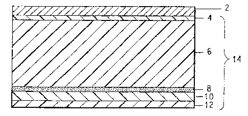
In one embodiment, illustrated in Figure 1, a multilayer polyimide
and fiuoropolymer-substrate 14 in accordance with the present invention is
sealed around a wire or cable 2. In this embodiment, the polyimide core
layer 6 generally provides the dielectric substrafie ~,rith mechanical
2o toughness and dielectric strength at high temperatures. The optionai
pofyimide-to-metal (P T ~) layer 4 generally provides improved adhesion of
the polyimide core layer to the metal wire or surface. The optional
adhesive primer layer 8 generally provides improved adhesive strength
between the high-temperature bonding layer 10 and the polyimide core
2s layer 6. The high-temperature bonding Payer 10 generally provides for
improved mechanical resistance to scrape abrasion and cut through. The
optional outer PTFE layer 12 generally provides improved thermal aging
resistance, chemical resistance, and resistance to electrical arc tracking.
In one embodiment, the polyimide-to-metal ("PTM") bonding layer,
~o polyimide core layer and the adhesive primer layer are formed into a three
layer film, where the fluoropolymer layers are eacl-9 coated onto the
polyimide layer as an aaueous dispersion. in addition, the high-
temperature bonding layer is generally applied to one side of this three-
layer laminate {also by aqueous dispersion). The resulting four-layer
~s dielectric substrate can then be cut into tapes and spiral wrapped around a
wire, cable or other electrical conductor. Thereafter, an outer layer
comprising a PTFE base polymer Layer can be applied separately as a
porous, sinterable laminate tape and then partially or wholly sintered (and
CA 02473824 2004-07-13
heat-sealed) generally under high temperature to wholly or partially densi'ry
and adhere the PTFE exterior Layer to tt~e other layers of fhe present
invention.
Qptional Innermost Layer (Polyimide-to-Metal or "PTM"' E~ondinq Layer):
s Particularly in wire/cabie wrap applications, the optional polyimide-
to-metal ("PTM") bonding layer is oftentimes used as the innermost Layer,
generally intended for placement substantially adjacent tn an electrically
conductive wire (or cable) located substantially at the center of a wrapped
system. In a typical wire/cable wrap application, the wrapped conductive
to elePinent generally comprises copper wire having a metal coating that
serves to protect the copper from oxidation. The metal coating is
oftentimes a high purity tin (typically applied by electroplating), where the
conductive element has an operating temperature rating of up to150°C.
For higher temperature ratings (up to 200°C), sliver is often used
rs and for ratings up to 260°C, a nickel coating is generally used.
Though
the metal coating may be applied by dipping or other electroless method,
the stranded copper wire is typically electroplated, and therefore will be
described throughout as being plated with tin, silver or nickel.
Preferably, the polyirnide-to-metal (''PTM") banding Payer is heat
2o sealed or otherwise reliably bonded to the conductor material as part of
the wirelcable wrap process. Ordinary skill and experimentation may be
necessary in selecting the particular polyimide-to-metal ("PTM") bonding
layer that (optimally) bonds to a particular conductive element to be
wrapped.
2s In one embodiment, a FEP base polymer is used as a substantial
(or entire) portion of the polyimide-to-metal ("PTM") bonding layer. fn
other embodiments, the palyimide-to-metal ("PTM") bonding Layer will
generally have a base polymer comprising about 50, 60, '70, 80, 90, 95,
96, 97, 98,99, 99.5 or 100 weight percent FEP. Additional polymeric
constituent(s); if any, comprise other fluoropolymers including, but not
limited to, polytetrafluoraethylene (PTFE), poiy(tetrafluoroethyiene-co-
perfiluoro[alkyl,vinyl etherj) (PFA) and poly(ethylene-co-tetrafluoroethylene}
(ETFE).
The poiyimide-to-metal ("PTM") bonding Payer is preferably from
~s about 0.25, 0.3, 0.4, 0.5, 0.-l5, 1, 2, 3, 4, or 5 to abo!,~t 15, 20, 22 or
25.0 microns thick, mare preferably from 8, 10 or 12 to about 14, 15, 16 or
17 mPCrOrlS thick.
6
CA 02473824 2004-07-13
The Polvimide Core Laver:
In one embodiment, the second layer (counting in the radial
direction outward from the electrical conductor) the dielectric substrate, or
laminate system; comprisEa one or more polyimides as the base polymer.
s This polyimide layer is generally referred to herein as the "core layer" or
"polyimide core layer".
Generafiy, the polyirnide core layer should be thick enough to
provide electrical insulation properties and structural strength. However,
the polyimide core layer generally must also be thin enough to be flexible
to and easily (and closely) molded to the article to be wrapped. Hence, the
polyimide core layer will generally have a thickness in a range between
(and including) any two of the following thicknesses (microns): 8, 108 12,
15, 20, 25, 30, 40, 50, 60, °70, i5, 80, 90, 95, 100, 120, '125, 130,
135,
140, 145 and 150. In ane embodiment, the core layer will be about 10 to
Is 25 microns thick (e.g. 15 microns).
The polyimide core layer is generally derived from a poiyamic acid
precursor. The polyamic acid precursor can also comprise conventional
(or non-conventional) catalysts andlor dehydrating agent(s). Methods for
converting polyamic acid solutions into polyimide films are well known in
zo the art and need not be discussed further here. Ar~y conventional or non=
conventional method for manufacturing pofyimide film can be used to
manufacture the care Eayer of the present invention.
In one embodiment, a polyamic acid precursor of about 5 to
40 percent by weight polymer solution dissolved in an organic solvent,
2s according to methods Vvell known in the art of polyimide film manufacture.
The polyamic acid solution further comprises dehydrating agents, such as
aliphatic acid anhydrides (acetic anhydride, etc.) or aromatic acid
anhydrides. In such an embodiment, catalysts such as aliphatic tertiary
amines (triethylamine, etc.), aromatic tertiary amines (dirhethylaniline, etc)
and heterocyclic tertiary amines (pyridine, picoline, isoquinoline, etc) are
added to speed the drying process of the acid into a freestanding film. In
such an embodiment, the dehydrating material can be used in slight molar
excess, relative to the amount of amide acid groups in the polyamic acid.
In This particular embcdiment, about 2.0 to 3.0 motes of dehydrating
3s material (per equivalent of polyamic acid) are useful. Generally, a
comparable amount of tertiary amine catalyst is al:>a useful.
In these embodiments, the polyamic acid solution is the (direct or
indirect) reaction product o~f diamines and dianhydrides (or precursors or
7
CA 02473824 2004-07-13
derivative thereof) dissolved in a polar solvent. Common diamines useful
to make the poiyimides of t:he present irwention include:
1. 2,2 bis-(4-amin,ophenyl) propane;
s 2. 4,4'-diaminodiphenyl methane;
3. 4,4'-diaminodiphenyl s~ilfide (4,4'-DDS);
4. 3,3'-diaminodipheny) sulfone (3,3'-DDS);
5. 4,4'-diaminodiphenyl sulfone;
6. 4,4'-diaminodiphenyl ether (4,4'-ODA);
7. 3,4'-diaminodiphenyf ether (3,4'-ODA);
8. 1,3-bis- (4-aminophenoxy) benzene (APB~134);
9. 1,3-bis- (3-amirto~heno>;y) benzene (APB-133);
10. 1,2-bis- (4-aminophenoxy) benzene;
11. 1,2-bis- {3-amir~ophenoxy) benzene;
1s 12. 1;4-bis-(4-aminophenoxy) benzene;
13. 1,4-bis-(3-aminophenoxy) benzene;
14. 1,5-diaminoriaphthalene;
15. 1,8-diaminonaphthalene;
16. 2,2'-bis(trifluoromethyibenzidine)
'17. 4,4'-diaminodiphenyldiethylsilane;
18. 4,4'-diaminodiphenylsilane;
7 9. 4,4'-diaminodiphenylethylphosphine oxide;
20. 4,4'-diaminodiphenyl-~I-methyl amine;
21. 4,4'-diaminodiphenyl-N-phenyl amine;
22. 1,2-diaminobenzene (OPD);
23. 1,3-diaminobenzene {MPD);
24. 1,4-diaminobenzene (PPD);
25. 2,5-dimethyl-1,4-diaminobenzene;
26. 2-(trifluoromethyl)-1;4-phenyfenediamir~e;
27. 5-(trifluoromethyl)-1,3-phenylenediamine;
28. 2,2-Bis[4-(4-aminopnenoxy)phenyl]-hexafiuoropropane;
29. 2,2-bis(3-aminophenyl) 7,1,1,3,3,3-hexaffuoropropane;
30. benzidine;
31. 4,4'-diaminobenzophenone;
3s 32. 3,4'-diaminobenzophenone;
33. 3, 3'-diaminobenzophenone;
34. m-xyfylene diamine;
35. bisaminophenoxyphenylsulfone;
8
CA 02473824 2004-07-13
36. 4,4'-isopropyiidenedianiiine;
37. N,N-bis- (4-aminophenyl) methyiamine;
38. N,N-bis- (4-arr;inophenyl) aniline
39. 3,3'-dimethyl-4,4'-diaminobiphenyl;
s 4Q. 4-aminophenyl-3-aminobenzoate;
41. 2,4-diaminotoiuene;
42. 2,5-diaminotofuene;
43. 2,6-diaminotoluene;
44. 2,4-diamine-5-chlorotoluene;
l0 45: 2,4-diamine-6-chlorotoluene;
46. 4-chloro-1,2~phenylenediamine;
47. 4-chloro-1,3-phenylenediamine;
48. 2,4-bis- (beta-amino-t-butyl) toluene;
49. bis- (p-beta-amino-t-butyl phenyl) ether;
Zs 50. p-bis-2- (2-methyl-4-aminopentyl) benzene;
51. 1-(4-aminophenoxy)-3-(3-aminophenoxy) benzene;
52. 1-(4-aminophenoxy)-4-(3-aminophenoxy) benzene;
53. 2,2-bis-j4-(4-aminophenoxy)phenyl] propane
(BAPP);
54. bis-j4-(4-aminophenoxy)phenyi] sulfone (BAPS);
20 55. 2,2-bis[4-{3-aminophenoxy)phenyl] sulfone
{m-BAPS);
56. 4,4'-bis-(aminophenoxy)biphenyl (BAPB);
57. bis(4-j4-aminophenoxy)phenyl) ether (RAPE);
58. 2,2'-bis-(4-aminophenyl)-hexafluoropropane
(6F diamine);
59. 2,2'-bis-(4-phenoxy aniline) isopropylidene;
2s 60. 2,4,6-trimethyl-1,3-diaminobenzene;
61. 4,4'-diamino-2,2'-trifluoromethyi diphenyloxide;
62. 3,3'-diamino-5,5'-trifluoromethyl diphenyfoxide;
63. 4,4'-trifluoromethyl-2,2'-diaminobiphenyi;
64. 4,4'-oxy-bis-j(2-trifiuoromethyl) benzene
amine];
65. 4,4'-oxy-bis-j(3-trifluoromethyl) benzene
amine];
66. 4,4'-thio-bis-j{2-trifluoromethyl) benzene-amine];
67. 4,4'-thiobis-j(3-frifluoromethyl) benzene
amine];
68. 4,4'-sulfoxyl-bis-j(2-trifluoromethyl) benzene
amine;
69. 4,4'-sulfoxyl-bis-j(3-trifluoromethyl) benzene
amine];
3s 70. 4,4'-keto-bis-j(2-trifluoromethyl) benzene
amine];
71. 9,9-bis(4-aminophenyl)fluorene;
72. 1, 3-d iamino-2,4, 5, 5-tetr of iuor obenzene;
9
CA 02473824 2004-07-13
73. 3,3'-bis(trifluoromethyl)benzidine;
and the Pike.
Common dianhydrides useful to make fhe polyamic acids (and after
s drying and curing the polyimides of the present invention) include:
1. pyromellitic dianl~ydride (PiVfDA);
2. 3,3',4,4'-biphenyl tetracarboxy(ic dianhydride (BPDA);
3. 3,3',4,4'-benzophenone tetracarboxylic dianhydride (BTDA);
4. 4,4'-oxydiphthalic anhydride (ODPA);
5. 3,3',4,4'-diphenyisulfone tetracarboxylic dianhydride (DSDAI;
6. 4,4'-(4,4'-isopropylidenediphenoxy)bis(phthalic anhydride) (BPADA);
7. 2,3,6,7-naphthalene tetracarboxyfic dianhydride;
8. 1;2,5,6-naphthalene tetracarboxylic dianhydride;
9. 1,4,5,8-naphthalene tetracarboxylic dianhydride;
1s 10. 2,6-dichloronapilthalene-1,4,5,8-tetracarboxyfic dianhydride;
11. 2,7-dichioronaphthalene-1,4;5,8-tetracarboxylic dianhydride;
12. 2,3,3',4'-biphenyl tetracarboxylic dianhydride;
13. 2,2',3,3°-biphenyl tetracarboxylic dianhydride;
14. 2,3,3',4'-benzophenone tetracarboxylic dianhydride;
15. 2,2',3,3'-benzophenone tetracarboxylic dianhydride;
16. 2,2-bis(3,4-dicarboxyphenyl) propane dianhydride;
17. 1,1-bis(2,3-dicarboxyphenyl) ethane dianhydride;
18. 1,1-bis(3,4-dicarboxyphenyl) ethane dianhydride;
19. bis(2,3-dicarbo;~yphenyl) methane dianhydride;
2s 20. bis(3,4-dicarboxyphenyl) methane dianhydride;
21. 4,4'-(hexafluoroisopropylidene) diphthaiic anhydride (6FDA);
22. bis(3,4-dicarbaxyphenyl) sulfoxide dianhydride;
23. tetrahydrofuran-2,3,4,5-tetracarboxylic dianhydride;
24. pyrazine-2,3,5,6-tetracarboxylic dianhydride;
25. thiophene-2,3,4,5-tetracarboxylic dianhydride;
26. phenanthrene-1,8,9,10-tetracarboxylic dianhydride;
27. perylene-3,4,9,10-tetracarboxyiic dianhydride;
28. bis-1,3-isobenzofurandione;
29. bis (3,4-dicarboxyphenyl) thioether dianhydride;
ss 30. bicyclo[2.2.2)oct-7-ene-2,3,5,6-tetracarboxylicdianhydride;
31. 2- (3',4'-dicarboxyphenyl) 5,6-dicarboxybenzimidazole dianhydride;
32. 2- (3',4'-dicarboxyphenyl) 5,6-dicarboxybenzoxazole dianhydride;
33. 2- (3',4'-dicarbo;~cypheny() 5;6-dicarboxybenzofhiazole dianhydride;
CA 02473824 2004-07-13
34, bis (3,4-dicarboxyphenyl) 2,5-oxadiazole 1,3,4-dianhydride;
35. bis 2,~-(3',4'-dicarboxydiphenylether) 1,3,4-oxadiazole dianhydride;
36. and the f ike;
37. their acid ester and their acid chloride derivatives.
J
In one embodiment, the prefierred diamines to form the polyamic
acid are 4,4'-diaminodiphenyl ether and p-phenylene diamine. The
preferred dianhydrides are pyromellitic dianhydride and 3,3'4,4'-
biphenyltetracarboxylic dianhydride. Generally, the resulting polyimide
to films formed therefrom are sufficiently flexible to conform as a wire wrap
core layer white also having advantageous modules and mechanical
toughness compared to many other polymer (and poiyimide) systems.
Useful commercially available polyimides core layers include
Kapton~ films, available for E.l. du Pont de Nemours and Company of
is Wilmington, Delaware, USA. In particular, any high modules Kapton~ film
(meaning a film with greater than 700 kpsi modules) is generally
wparticularly useful, due to the desirable mechanical toughness. However,
other polyimide films, fln-~s with lower rr;odulus, may also be used.
The polyimide core layer may have its surface modified to improve
2o adhesion of the core layer to other layers. For example, prior to applying
a
pofyimide-to-metal bonding layer or adhesive primer layer using an
aqueous dispersion coating technique, the polyimide film can be subjected
to a pre-treatment step. These pre-treatments steps include, but are not
limited to, corona treatment, plasma treatment under atmospheric
2s pressure; plasma treatment under reduced pressure, treatment with
coupling agents like silanes and titanates, sandblasting, alkali-treatment,
and acid-treatment. Such pre-treatment steps are well known in the art
and need not be discussed further herein.
To improve the adhesion strength between the core layer and the
so adjacent bonding layers, it i's also possible to add vrarious organic
andlor
inorganic metal compounds (e.g. metal oxides andlor rnetai complexes).
Addition of these metal compounds is disclosed for example in U.S. Patent
No. 4,T42,099 (tin compounds, titanium compounds, etc.). Commonly,
these metal compounds are added to the polyamic acid or are applied to
ss an uncured wet film. Addition of organic compounds, used to improve
adhesion strength between the core layer and the adjacent bonding
layers, is discussed in U.S. patent application Ser. No. 10/150,233 entitled
" A Laminate Structure ~llade From a Highly Dondabie Polyimide, s he
11
CA 02473824 2004-07-13
Laminate Structure Exhibiting Improved Adhesive Strength" pending, filed
May 77, 2002 and U.S. patent application Ser. No. 091848,895 entitled
"Polyimide Composition Having improved Peei Strength With Clad",
pending, filed 05/04/2001.
s The Optional Adhesive Primer Layer and Poiyimide-to-Metal (PTM) Layer
In accordance with one embodiment of the present invention, the
poLyimide core layer's exterior surfaces are optionally coated with an
adhesive primer layer and a polyimide-to-metal bonding layer.
The polyimide-to-metal ("PTM") bonding Layer and the adhesive
zo primer layer can be the same or different, provided however that each
comprise about 50, 60, 70, 80, 90, 95, 96, 97, 98, 99, 99.5 or 100 weight
percent FEP. Additional polymeric constituent(s), if any, comprise other
ffuoropolymers including, but not limited to, polytetrafluoroethylene
(PTFE), poly(tetrafluoroethylene-co-perfluoro[alkyl vinyl etherl) (PFA) and
15 poly(ethylene-co-tetrafluaroethylene) (ETFE).
The adhesive primer Layer and the polyimide-to-metal bonding layer
are preferably from 0.25, 0.5, 0.75, 1, 2, 3, 4, or 5 to 6,8,1fl, 12, 14, 16,
18;
20, 22 or 25 microns thick, and in one embodiment from 8, 10 or 12 to 15,
i 6 or 17 microns thick.
2o In one embodiment, the polyimide-to-metal {"PTM") bonding layer
and the adhesive primer Layer can be conveniently applied to the
polyimide core Layer as an aqueous dispersion comprising a colloidal FEP
polymer. The applied dispersion will generally have a thickness from
about 0.02, 0.05. 0.075, or 0.1 to about 0.12, 0.13, 0.14, or 0.15 mil {about
25 0.5 to about 3.75 microns).
Oftentimes, these layers will be applied from 0.03 to 0.06 mil {about
0.75 to about 1.5 microns) thick. The double side coated polyimide film
can then be heated to a temperature in a range from about 325°C to
about
450°G (preferrably 370°C to 450°C) for about 0.25 to 5
minutes.
30 The optional adhesive primer layer can be specifically designed so
that the bonding temperature of that layer to the adjacent polyimide Layer
is low (i.e. in a range between and including any two of the following
temperatures 375°G, 380, 385, 390, 395, 400, 405, 410, 415, 420 and
425°C). .
ss In many embodiments, a bonding temperature in a range of
between 400 to 410°C can be particularly useful. Oftentimes, optimum
banding temperatures are below 425°C so that the polyimide layer is not
degraded during construction of the overall Laminate.
12
CA 02473824 2004-07-13
The optional adhesive primer layer (e.g., FEP) generally provides
excellent bonding of the poiyimide core layer and the subsequently applied
high-temperature bonding layer , In addition, the polyimide-to-metal layer
provides excellent bonding of the polyimide care layer to the wire,
s electrical conductor, or metal substrate.
The polyimide-to-metal (PTM} layer can also be used in the
multilayer structures of the present invention to facilitate stripping of fhe
insulation from the electrical conductor when used in commercial
applications.
to Hiah-Temperature Bondin Lc~ ayer:
The high-temperature bonding Layer is also referred to herein as the
polyimide-to-fiuoropolyrr~er ("PTF'y) bonding layer in cases where the
(optional) fluoropofymer exterior layer is applied. The resulting PTF
bonding Layer (or high temperature bonding Payer) provides improved
Zs bonding performance between the exterior fluoropoiymer layer (e.g. PTFE)
and the interior polyimide core layer. The PTF bonding layer is preferably
PFA, and may optionally be blended w°ith FEP fluaropoiymer. The
PTF
bonding layer provides the dielectric substrate wifh excellent resistance to
mechanical degradatiar~, especially scrape abrasion and cut-through.
2o In one preferred embodiment, tl7e high-temperature banding layer
(or the PTF Layer) is optionally blended with FEP to form a PFA/FEP
blended fluoropolymer. The high-temperature banding layer has at least
~40, ~5, 50, 55, 60, 65, '~0, 75, 80, 85, 90, 95, or '100 weight percent of
PFA
copolymer. However, up to 60 weight percent of the high-temperature
2s bonding layer may be FEP or a_fluoropolymer selected from the group
consisting of polytetrafluoroethyiene (PTFE) and poly{ethylene-co-
tetraffuoroethylene) (ETFI=).
In one embodiment, the PFAIFEP blend consists of from 50, 55, 60,
65, or 70 wt. percent to about 75,80, 85 or 90 percent by weight PFA. In
this embodiment, the FEP copolymer ranges from 10, 15, 20 or 25 to 30,
35, 40, 45 or 50 weight percent.
Suitable FEP copolymers useful as a blend components are
commercially available as TefIonT"" TE-5582, TefianTM TE-9503, and
T effonTM 720, available from E. I. du Pont de f~emours & Company,
ss Wilmington, Delaware, USA.
PFA may be derived from aqueous dispersion of a commercial PFA
material, such as Teffon0 322J, available from E.l. du Pont de Nemours
and Company of Wilmington, DE, USA.
13
CA 02473824 2004-07-13
The PTF bonding layer (e.g., PFAIFEP blend layer) can be
subsequently applied to the adhesive primer layer (FEP) or directly to the
polyimide core layer as a colloidal aqueous dispersion. These dispersions
typically have a solids content of from about 5, 10, 15, 20 or 25 weight
s percent to about 30, 35, ~.0 ~5, 50, 55; or 60 weight percent. Thereafter
heating is applied to the dispersed layer from 350°C to 500°C
for about
0.50 to 5 minutes.
For the PTF bonding layers (or high temperature bonding layers) of
the present invention, the PFA should generally have a melting point in a
to range between (and including) any two of the following temperatures
(°C):
220, 225, 230, 240, 250, 260, 270, 280, 290, 295, 300, 305, 310, 315 and
320°C.
The PTF bonding layer (e.g., PFAIFEP layer) may be applied by
either coating or iaminatior~ techniques.
is The PTF bonding iae~er (or high-temperature bonding (aver) will
generally have a thickness in a range between (and including) any two of
the following thicknesses (in microns): 0.25, 0.3, 0.~, 0.5, 0.6, 0.7, 0.8,
0.9,
1.0, 1.25, 1.5, 1.75, 2, 3, 4, 5, 10, '11,12, 13, 14, 15, '16, ~17, 18, 19,
20,
21, 22, 23, 24 and 25 microns. A useful thickness range is oftentimes in a
range from about 0.75 microns to 2.5 microns (generally in the range of
about 0.03 to about 0.10 mils). in practice, the desired~thickness can
depend upon the particular wire specifications, particularly for military or
commercial aircraft applications.
In one embodiment, the high-temperature bonding layer contains
2s 90 weight percent PFA where the remainder is FEP. This particular
formulation improves the peel strength for the overall laminate structure.
The peel strengths of the laminate structures using the fCrst e~cterior
layer described above showed peel strengths greater than or equal to 2, 3,
4, 5, 6, 7, 8, 9, or 10 pounds per linear inch ("pfi").
The improved peel values observed at room temperature (as a
result of using the first exterior layers described above) generally correlate
to improved bond values o~f the overall laminate structure at extreme
temperature conditions. Extreme high and tow temperature conditions are
typically encountered in certain high performance (i.e., aerospace and
~s aircraft) applications where wire wrap compositions are heated and cooled
very rapidly. The improved peel strengths discovered in the laminates of
the present invention also dorovide improved resistance to scrape abrasion
14~
CA 02473824 2004-07-13
and ease of stripping of the laminate system from a wire without
delamination of individual layers.
Improved scrape abrasion resistance (i.e. improved resistance to
ultimate mechanical failure of the insulation system) generally can be
s particularly useful in applications where unwanted electrical arc tracking
(seen when the insulation is mechanically degraded) is of great concern.
The Exterior sayer:
In accordance with one embodiment of the present invention, the
PTF bonding layer,.the polyimide core layer, and optional adhesive primer
layer ardd polyimide-to-metal layer is generally applied to the wirelcable as
a wrapped tape. Next, typically in the opposite direction, the exterior layer
is also wrapped around the already insulated elects ical conductor.
In this erribodiment, the exterior layer comprises a sintered or
sinterable fluoropolymer base polymer, such as, polytetrafluoroethylene
is {"PTFE"). PTFE layers can be useful due to their high melting point.
While a pure PTFE layer can provide a melting point greater than
300°C,
other fluoropolymers may be blended with the PTFE to obtain a variety of
desired properties. Typically, the viscosity of the PTFE is a range on the
order of from about 108 GPa-s to 10~~ GPa~s, more preferably from about
10~o GPa~s to 1012 GPa~s, most preferably 1011 GPa~s. I
Other possible fiuoropolymers that can optionally be blended with
the PTFE include FEP, PFA, ETFE, and other thermally compatible TFE
copolymers.
The exterior Gayer can also be a copolymer made of
2s hexafluoropropylene and tetraffuoroethylene (FEP) comprising about 5 to
50 weight percent hexafluoropropylene and about 95 to 50 weight percent
tetrafluoroethylene.
The exterior layer will generally provide some scrape abrasion
resistance, chemical resistance, and thermal durability when the structure
3o is wrapped about a wire or cable or the like. Used as an exterior layer,
the
thickness is generally from 1 to 200 microns. Useful thicknesses are
generally from about 2, 5, 7, 10, 15, or 25 to about 30, 35, ~40, 45 or 50
mrcrons.
Filler Materials:
~s in some embodiments of the present invention, additives can be
incorporated into one or more of the laminate fluoropolymer layers, or the
polyimide core layer, to improve the performance of any particular layer at
elevated temperatures. Useful additives include minerals having outgas
CA 02473824 2004-07-13
properties at the temperature of an electrical arc, such as carbonates that
evolve carbon dioxide (e.g", calcium or magnesium carbonate, or hydrated
fillers or minerals containing water). Other useful additives may include
alumina oxide, titanium dioxide, fumed a(umina oxides, carbon, electrically
s conductive powders, elec~ricalfy conductive polymers and the like.
Yet, other potentially suitable additives would include polymers
which; like PTFE itself, decompose without producing carbonaceous or
other conductive by-products upon decomposition. These additives may
be incorporated into the fluoropolymer layers of the claimed composite,
to particularly in that layer nearest the conductor to be insulated.
For example, one or more pigments may be incorporated into any
of the fluoropo(ymer layers or the polyimide core layer, such as, for
purposes of laser marking. Such pigment may comprise 3 to i5% by
weight or' a fluoropolymer film (or layer), preferably 4 to 1 n% by weight,
is and most preferably ~. to 8% by weight. For example, an exterior
fluoropolymer layer made of 1'TF' may be used which incorporates one
pigment to make the layer white laser markable.
Alternatively, two la)rers can be used for this purpose, each
incorporating different pigments of contrasting colors. ~.aser etching of the
20 outermost pigmented layer could then reveal the contrasting color for
identification of the wire type. !n some embodiments, the outermost
pigmented layer should not be thicker than about 8 microns in order to
obtain sharp definition of the identifying code at the energy density of
lasers presently commercially available.
2s Forming an Electrically fnsulative Tane and Wrap~~n~ a llVire or
Conductor:
The dielectric substrates of the pr esent invention are generally
useful for electrical insulation purposes. The structures can be slit into
narrow widths to provide tapes. These tapes can then be wound around
3o an electrical conductor in spiral fashion or in an overlapped fashion. The
amount of overlap can vary, depending upon the angle of the wrap. The
tension employed during the wrapping operation can also vary widely,
ranging from JUSt enough tension to prevent wrinkling, to a tension high
enough to stretch and neck down the tape.
3s - Even when the tension is low, a snug wrap is possible since the
tape will often shrink under the influence of heat during any ensuing heat-
sealing operation. Heat-sealing of the tape can be accomplished by
treating the tape-wrapped e:onductor at a temperature and time sufficient
16
CA 02473824 2004-07-13
to fuse the high-tempera~ure bonding layer to the other layers in the
composite.
The heat-sealing ternperature required ranges generally from 240,
250, 275, 300, 325 or 350°C to 3 r 5, 400, 425, 450, 475 or
500°C,
s depending upon the insulation thickness; the gauge of the metal
conductor, the speed o. the production line and the length of the sealing
oven.
EXAMPLES
The insulated ~nrires in the following EXAMPLES were tested for
to several properties including resistance to scrape abrasion and lamination
adhesion strength between the polyimide and fluoropolymer layers.
Resistance to mechanical scrape abrasion is measured using a
piece of equipment similar to equipment made available by General
Electric sold as a Repeated Scrape Abrasion Tester, Cat. No.158I238G ~ .
Is In the EXAMPLES below, the scrape abrader was fitted with a 0.5-mm
(0.019-inch) diameter abrading mandrel. T he weight applied to the
mandrel was 800 grams. The wire was positioned in the testing
equipment and the equipment was started. The number of 'cycles'
needed to remove the insulation and expose the conductor was recorded
2o as the scrape abrasion number.
The present inventor has found that adhesion strength in the
dielectric substrate laminate directly correlates to performance in scrape
abrasion resistance as well as the overall usefulness of fhe dielectric
substrate as an insulative vrrap for wire and a substrate for an electronic
2s device.
The test method below is used to measure the adhesion between
various layers of certain polyimide-fluoropofymer laminate structures and
is herein referred to as the "adhesion test method". This i:est uses a
robatic heat-sealing device (similar to Pack Rite Machines Model RT) and
a tensile tesfing machine (similar to Instron Model 1122).
Test materials ar a cut into long narrow strips approximately
six inches Tong and one inc~~ wide. The strips are positioned one directly
on top of the other. This is called a test stack. One end of the test stack
(approximately one-inch long) is placed in a robotic heat sealer where it is
~s pressed between two heated metal bars. The pressure betv~reen these
bars, the temperature of the bars, and the time that the pressure is applied
to the bars, are all carefully controlled. The test stack is pressed together
and removed from the heat sealer. The test specimen has one f used end
1~
CA 02473824 2004-07-13
with a strip ofi each lamination test material protruding outward from the
sealed material.
Next, the test specimen is mounted in a tensile testing machine by
attaching one of the "free" ends of. the lamination strips to one jaw, and the
s other free end of the lamination strips to the other jaw. The tensile tester
is then started and the jaws begin to move in opposing directions. During
this time the tensile force between the jaws is measured and recorded.
The tensile force represents the adhesion between the various
laminate layers (i.e. higher adhesion values will give higher tensile force
to values). The highest tension value is selected and reioorted as the
adhesion value for the specimen. Normally, five specimens are tested and
the average of the five becomes the reported adhesion value of the test
materials.
Nothing within the foregoing discussion is intended to limit the
is present invention. Rather, the scope of the present invention is intended
exclusively according to the: following claims beiovtr.
PXAAAPi F "I
A polyimide-fluoropoiymer insulation tape having a high modulus
polyimide film layer, a high-temperature bonding layer made from a blend
20 of PFA and FEP, and adjacent adi~esive primer layer and a polyimide-to-
metal (PTM) layer made of FEP, and a sintered PTFE layer adjacent to the
high-temperature bonding 4ayer was constructed.
The polyimide film thickness was nominally 0.65 imils in thickness
and had a moduius over X00 kpsi.
2s A thin layer of aqueous based fluorinated ethylene-propylene
(FEP), approximately 0.07 mils thick (final dry thickness) was applied to
bath sides of the pofyimide f ilm layer to form both the adhesive primer
layer and the pofyimide-to-metal (PTM) layer on the pofyimide layer.
These two coating layers were fused to the polyimide film using a vertical
radiant-heat, curing oven at a maximum film temperature of ~-'( 0°C.
A layer containing 10 % by weight FEP and 90% of perfluoroalkoxy-
fluorocarbon (PFA) was coated over the adhesive primer layer as an
aqueous solution to form a high-temperature bonding layer. The high-
temperature bonding layer was approximately 0.07 mils thick. Next, the
~s polyimide layer (and adhesive primer layer and polyimide-to-metal Payer)
and the high-temperature bonding layer was cut into a tape and wrapped
around a wire.
18
CA 02473824 2004-07-13
The wire conductor was a 24 AV'~G nickel-plated 19-36 stranded
conductor. The electrically insulative tape was applied to the conductor in
spiral wrapped manner to allow the tape to overlap itself by more Than
50% forming "double-layer" insulation.
Next, unsintered PTFE tape, measuring 2.0 mils in thickness, was
layered onto the coated v~ire as a tape. The PTFE was adhered to the
high-temperature bonding layer using heat and pressure. The PTFE tape
was white laser markable. 'The PTFE outer tape was applied in much the
same manner as the first tape except it was applied in the opposite
zo direction (cross-v,rrapped).
The heating process was completed in an electric r adiant vertical
oven, 10 feet in heighfi, wish air temperatures ranging from 480 to
540°C.
The processing speed of the coated wire through the oven was about
40 feetlminute.
zs The average number scrape abrasion cycles of EXAMPLE 1 was
111 cycles. This number represents an increase of approxirnatefy 20% in
scrape abrasion compared to similar wires made using high tensile
strength polyimide and standard FEP coatings.
EXAMPLE 2
20 EXAMPLE 2 was constructed as a laminate system and was not
wrapped onto a wire. The difference befiween EXAMPLE 2 and EXAMPLE
1 is discussed below. in EXAMPLE 2, a four-layer composite was
laminated to an exterior P T FE layer. The four-layer composite consisted
of two coating layers (i.e. the adhesive primer layer and the polyimide-to-
2s metal (PTM) layer), the polyimide core layer, and the high-temperature
bonding layer (PFAIFEP). These four Payers were fused to an exterior
layer (PTFE) at a maximum vlm temperature of 375°C, at r 0 psi, for
seconds. However, the five-layer composite was not wrapped around a
wire but kept as a sheet laminate.
3o The pee( strength of the overall laminate structure, without the wire
conductor, was measured at 1988 glin. according to the adhesion test
method.
EXAMPLE 3
EXAMPLE 3 was constructed in accordance with EXAMPLE 2. The
3s difference regarding EXAMPLE 3 is that the lamination conditions had a
maximum film temperature of 375°C, at only 3 psi, far 10 seconds.
19
CA 02473824 2004-07-13
The peel strength of the overall laminate structure, without the wire
conductor, was measured at '( 759 g/in. according to the adhesion test
method.
- COMPARATIVE EXAfvtPLE 1
The electrically insulative substrate of this GOMPARATITVE
EXAMPLE was prepared in accordance with EXAMPLE 1 (i.e. wrapped
around a wire and measure for scrape abrasion resistance) except for the
following.
A thin layer, approximately 0.10 mils thick (final dry thickness) of
to aqueous based fluorinated ethylene-propylene (FEP) was applied to both
sides of the polyimide material to form the poiyimide-fo-metal (PTM) layer
and a ''bonding layer" made of pure FEP (no PFA). The "bonding layer"
took the place of both the adhesive primer layer and the high temperature
bonding layer (the PTF layer) of EXAMPLE 1.
zs The coating fayers were fused to the polyimide film using a vertical
radiant-heated curing oven at a maximum film temperature of
approximately 410°C. The laminate was cut into tapes and wrapped
around a wire in accordance with EXAMPLE 1.
A PTFE tape, 2.O-mfl thsck (nominal} unsintered laser-markable
2o tape, was wrapped in the same manner as EXAMPLE 1.
The fused wire was tested for scrape abrasion resistance. The
average number of cycles to failure with this wire insulation was observed
to be in the range from 65 to 92 cycles.
COMPARATIVE EXAMPLE 2
2s COMPARATIVE EXAMPLE 2 was prepared in accordance with
COMPAP,ATiVE EXAMPLE 1. However, a thin layer, approximately
0.07 mils thick (final dry thickness) of aqueous based fluorinated ethylene=
propylene (FEP), with nc (PFA) was applied fio both sides of the poiyimide
f ilm. The coating layers were fused to the pofyimide film using a vertical
radiant heated curing oven at a maximum film temperature ~f
approximately 410°C.
Next, a second layer of aqueous based FEP fiuoropolymer was top
ccated over the adhesive primer layer of FEP. The thickness of the
topcoat layer was thus increased to the thickness of.approximately
3s 0.'14 mils. The electrically insulative composite was wrapped around a
wire in accordance with EXAMPLE 1.
CA 02473824 2004-07-13
The PTFE tape, 2.0-mil thick (nominal} unsintered laser-markable
tape, was wrapped around the insulated wire in accordance with
EXAMPLE 1.
The taped conductor was then exposed to a heating process to fuse
s the Pi-FP tape and sinter the P'i FE tape. This heating process was
completed in an electric radiant vertical oven, 1 Q feet in height, with the
air
temperatures inside of the oven ranging from 480 to 540°C. The linear
speed of the wire through the oven was 40 feetlminufe.
The fused wire was tested for scrape abrasion resistance. The
o average number of cycles to failure with this wire insulation was observed
as 89 cycles.
COMPARATIVE EXAMPLE 3
COMPARATIVE EXAMPLE 3 was prepared in accordance with
EXAMPLE 2 except that the nigh-temperature bonding layer did not
Is contain any PFA and was made purely of FEP copolymer. The maximum
film temperature used was in accordance with the lamination conditions o~
EXAMPLE 2. The lamination conditions were set at 375°C, 10 psi and
~ 0 seconds.
The peel strength or the overall laminate structure however, again
2o without the wire conductor, was measured at only 12'?5 glin. according to
the adhesion test method. This value is notably tower than the peat
strength number of EXAMPLE 2 (1988 g/in.}.
COMPARATIVE EXAMPLE 4
GOMPARATiVE EXAMPLE 4 was prepared in accordance with
zs EXAMPLE 3 except the maximum film temperature was set at 375°C,
3 psi, and 10 seconds. Again, the high-temperature bonding Layer (the
PTF layer} was pure FEP copolymer.
The peei strength of the overall laminate structure, without the wire
~coriductor, was measured at 1261 g/in. according to the adhesion test
so method. This value is notably iower-than the peel strength number of
EXAMPLE 3 (1759 glin}.
21