Note: Descriptions are shown in the official language in which they were submitted.
CA 02473939 2007-10-02
-1-
PCT/US03/00959
WO 03/63294
ENHANCED BANDWIDTH DUAL LAYER CURRENT SHEET ANTENNA
Background of the Invention
Technical Field
The present invention relates to the field of array antennas and more
particularly to array antennas having extremely wide bandwidth.
Description of the Related Art
Phased array antenna systems are well known in the antenna art. Such
antennas are generally comprised of a plurality of radiating elements that are
individually controllable with regard to relative phase and amplitude. The
antenna
pattern of the array is selectively determined by the geometry of the
individual
elements and the selected phase/amplitude relationship among the elements.
Typical
radiating elements for such antenna systems may be comprised of dipoles, slots
or any
other suitable arrangement.
In recent years, a variety of new planar type antenna elements have been
developed which are suitable for use in array applications. One example of
such an
element is disclosed in U.S. Patent No., 6,512,487 issued to Munk et al.
entitled
Wideband Phased Array Antenna and Associated Methods (hereinafter "Munk").
Munk discloses a planar type antenna-radiating element that has exceptional
wideband characteristics. In order to obtain exceptionally wide bandwidth,
Munk
makes use of capacitive coupling between opposed ends of adjacent dipole
antenna
elements. Bandwidths on the order of 9-to-1 are achievable with the antenna
element
with the Munk et al. design. Analysis has shown the possibility of 10-to-1
bandwidths achievable with additional tuning. However, this appears to be the
limit
obtainable with this particular design. Although the Munk et al. antenna
element ahs
a very wide bandwidth for a phased array
CA 02473939 2004-06-01
WO 03/063294 PCT/US03/00959
antenna, there is a continued need and desire for phased
array antennas that have even wider bandwidths exceeding
10-to-1.
Past efforts to increase the bandwidth of a
relatively narrow-band phased array antenna have used
various techniques, including dividing the frequency range
into multiple bands. For example, U.S. Patent No.
5,485,167 to Wong et al. concerns a multi-frequency phased
array antenna using multiple layered dipole arrays. In
Wong et al., several layers of dipole pair arrays are
provided, each tuned to a different frequency band. The
layers are stacked relative to each other along the
transmission/reception direction, with the highest
frequency array in front of the next lowest frequency
array and so forth. In Wong et al., a high band ground
screen, comprised of parallel wires disposed in a grid, is
disposed between the high-band dipole array and a low band
dipole array.
Wong's multiple layer approach has a drawback.
Conventional dipole arrays as described in Wong et al.
have a relatively narrow bandwidth such that the net
result of such configurations may still not provide a
sufficiently wideband array. Accordingly, there is a
continuing need for improvements in wideband array
antennas that have a bandwidth exceeding 10-to-
SUMMARY OF THE INVENTION
An array of radiating elements including a first set
of antenna elements in an array configuration and
configured for operating on a first band of frequencies,
and a second set of antenna elements in an array
configuration and configured for operating on a second
band of frequencies. The antenna elements can be planar
elements having an elongated body portion and an enlarged
-2-
CA 02473939 2004-06-01
WO 03/063294 PCT/US03/00959
width end portion connected to an end of the elongated
body portion. The enlarged width end portions of adjacent
ones of the antenna elements can have interdigitated
portions capacitively coupled to corresponding end
portions of adjacent dipole elements.
The first set of antenna elements are aligned in a
first planar grid pattern of spaced rows and columns and
the second set of antenna elements are aligned in a second
planar grid pattern of spaced rows and columns, the second
grid pattern can be rotated at an angle relative to the
first grid pattern, for example 45 degrees.
The first set of antenna elements is positioned below
the second set of antenna elements with the first set
acting as an effective ground plane for the second set.
The array can be configured for wideband operation by
having the first band of frequencies adjacent to the
second band of frequencies. The array can include a
dielectric material interposed between the first plurality
of antenna elements and the second plurality of antenna
elements.
The array can further include a set of first feed
organizers for communicating RF signals to the first set
of antenna elements and a set of second feed organizers
for communicating RF signals to the second set of antenna
elements. The first and second feed organizers are
arranged in a common grid pattern and extend upward toward
the antenna elements. A set of RF feeds of the second
feed organizers form a second feed organizer grid pattern
interposed on the common grid pattern. The RF feeds of
the second feed organizers extend through a plane
approximately defined by the first plurality of antenna
elements to communicate RF to the second plurality of
antenna elements. A ground plane can be positioned below
the first set of antenna elements, and a dielectric layer
-3-
CA 02473939 2004-06-01
WO 03/063294 PCT/US03/00959
can be interposed between the ground plane and the first
plurality of antenna elements.
BRIEF DESCRIPTION OF THE DRAWINGS
The various features and advantages of the present
invention may be more readily understood with reference to
the following drawings in which like reference numerals
designate like structural elements:
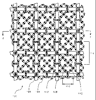
Fig. 1 is a top view of a dual band, dual layer
antenna array having a plurality of high frequency antenna
elements on a first layer and a plurality of low frequency
antenna elements on a second layer.
Fig. 2 is a cross sectional view, taken along line 2-
2, of the dual band, dual layer antenna array of Fig. 1.
Fig. 3 is a top view of a plurality feed organizers
embodied in the present invention.
Fig. 4 is an enlarged detail view of the layout of
the feed organizers of Fig. 3.
Fig. 5 is an enlarged cross sectional view of the
feed organizers of
Fig. 3.
Fig. 6 is a drawing illustrating an exemplary
wideband antenna element for use with the array of Fig. 1.
DETAILED DESCRIPTION OF THE INVENTION
Figs. 1 and 2 illustrate a dual-band, dual layer
antenna array 100. Fig. 1 is a top view of the array.
Fig. 2 is a cross-sectional view taken along line 2-2 in
Fig. 1. Array 100 includes of a plurality of low
frequency antenna elements 104 that are disposed on an
upper antenna surface 204 and a plurality of high
frequency antenna elements 102 that are disposed on a
lower antenna surface 202. The lower antenna surface 202
is positioned below the upper antenna surface 204. (The
-4-
CA 02473939 2004-06-01
WO 03/063294 PCT/US03/00959
high frequency elements 102 are shown in the top view of
Fig. 1 for clarity.) The antenna elements 102 and 104 can
be disposed on their respective surfaces 202 and 204 as
planar arrays, but the present invention is not limited as
other antenna element configurations can be used.
Array 100 can include a plurality of high frequency
feed organizers 208 and a plurality of low frequency feed
organizers 210. High frequency feed organizers 208
contact the high frequency antenna elements 102 at high
frequency feed points 106. Low frequency feed organizers
210 contact the low frequency antenna elements 104 at low
frequency feed points 108. The feed organizers 208 and
210 can be affixed to a surface 212. Optionally, a ground
plane can be positioned below the plurality of high
frequency antenna elements 102 and a dielectric layer can
be interposed therebetween.
An advantage of the present array configuration is
that the high frequency elements 102 can act as an
effective ground plane beneath the low frequency elements
104, thereby increasing the gain of the low frequency
antenna array without necessitating the use of a
conventional ground plane. The operational frequency
range of the ground plane created by the high frequency
elements 102 is determined at least in part by the spacing
110 between respective high frequency elements 102. The
upper end of the frequency range of the effective ground
plane increases as the spacing 110 is decreased. The
elements 102 can provide an effective ground plane
covering the frequency range from DC to the frequency
which has a wavelength approximately ten times the spacing
110.
Operationally, an image of the low frequency elements
104 is made by the effective ground plane, whereby the
effective ground plane can act as a reflector increasing
-5-
CA 02473939 2004-06-01
WO 03/063294 PCT/US03/00959
field strength pointing in an upper direction. The field
strength is in part a function of the distance 214 between
the effective ground plane and the plane of low frequency
elements 104. The particular distance 214 selected can be
determined by a variety of factors including the
operational frequency range of the low frequency elements
104, the desired impedance of the array 100, and the
dielectric constant of the volume defined between the
lower antenna surface 202 and the upper antenna surface
204. It should be noted, however, that some distances may
result in destructive interference and reduced field
strength in the upward direction, as would be known to one
skilled in the art.
In one embodiment, the distance 214 can be equal to
one-quarter of the wavelength of the highest operational
frequency for which the low frequency elements 104 will be
operated. Dielectric material 206 can be provided in the
volume defined between the lower antenna surface 202 and
the upper antenna surface 204. When dielectric material
206 is provided, the wavelength used for the one-quarter
wavelength computation can be equal to the wavelength of
the highest operational frequency as it propagates through
the dielectric inaterial 206. In alternate embodiments the
distance 214 can be determined using computer models and
adjusted to accomplish particular transmission or receive
characteristics.
The particular dielectric material 206 used in the
present invention is not critical and any of a variety of
commonly used dielectric materials can be used for this
purpose, although low loss dielectrics are preferred.
Further, the dielectric can be a gas, liquid or solid. A
dielectric having a dielectric constant greater than 1
reduces the recommended distance between the effective
ground plane and the low frequency elements 104 by
-6-
CA 02473939 2004-06-01
WO 03/063294 PCT/US03/00959
shortening RF wavelengths propagating through the
dielectric material 206. This enables the array 100 to be
more compact.
For example, one suitable class of materials that can
be used as the dielectric material 206 would be
polytetrafluoroethylene (PTFE) based composites such as
RT/duroid 6002 (dielectric constant of 2.94; loss
tangent of .009) and RT/duroid 5880 (dielectric constant
of 2.2; loss tangent of .0007). These products are both
available from Rogers Microwave Products, Advanced Circuit
Materials Division, 100 S. Roosevelt Ave, Chandler, AZ
85226. However, the invention is not limited in this
regard.
A further advantage of the array configuration shown
in Figs. 1 and 2 is that two antenna arrays having two
separate bands of frequencies are integrated to form a
single dual-band array. The frequency range of the high
frequency antenna elements 102 can be adjacent to the
frequency range of the low frequency antenna elements 104
so that the lower frequency range of the high frequency
el'ements 102 begins approximately where the response of
the low frequency antenna elements 104 cuts off. This
provides an antenna array system with an apparently wider
bandwidth than an array formed from a single type of
antenna element. Despite the advantages of the foregoing
arrangement, however, use of conventional narrow-band
antenna elements in such an array will still result in an
overall bandwidth that is somewhat limited. In
particular, the limited frequency range of the respective
high frequency and low frequency antenna elements used in
each array will limit the ultimate combined bandwidth of
the array.
The foregoing limitations can be overcome and further
advantage in broadband performance can be achieved by
-7-
CA 02473939 2004-06-01
WO 03/063294 PCT/US03/00959
proper selection of antenna elements. U.S. Application
Serial No. 09/703,247 to Munk et al. entitled Wideband
Phased Array Antenna and Associated Methods ("Munk et
al.), incorporated herein by reference, discloses such a
dipole antenna element. For convenience, one embodiment
of these elements for use as high frequency dipole pairs
is illustrated in Fig. 6. For example, the dipole pairs
can have an elongated body portion 602, and an enlarged
width end portion 604 connected to an end of the elongated
body portion. The enlarged width end portions of adjacent
ones of the antenna elements comprise interdigitated
portions 606. Consequently, an end portion of each dipole
element can be capacitively coupled to a corresponding end
portion of an adjacent dipole element. The low frequency
elements used in the array are preferably of a similar
geometry and configuration to that shown in Fig. 6, but
appropriately sized to accommodate operation in a lower
frequency band.
When used in an array, the dipole element of Munk et
al., has been found to provide remarkably wideband
performance. The wideband performance of such antenna
elements can be used to advantage in the present
invention. In particular, high frequency band and low
frequency band elements of the type described in Munk et
al can be disposed in an array as described relative to
Figs. 1 and 2 herein. Nevertheless, it should be noted
that the invention is not thus limited. Various types of
antenna elements can be used in the present invention.
For example, antenna elements that do not incorporate
interdigitated portions can also be used.
According to a preferred embodiment, first and second
sets of dipole antenna elements.can be orthogonal to each
other to provide dual polarization, as would be
appreciated by the skilled artisan. Referring to Fig. 1,
-8-
CA 02473939 2004-06-01
WO 03/063294 PCT/US03/00959
a plurality of high frequency dipole pairs 112 can be
aligned on the lower antenna surface 202 in a first grid
pattern of spaced rows and columns. A plurality of low
frequency dipole pairs 114 can be aligned on the upper
antenna surface 204 in a second grid pattern of spaced
rows and columns, as also shown in Fig. 1. Interference
between the two antenna layers can be minimized by
rotating the second grid pattern formed by the low
frequency dipole pairs 114 at an angle of approximately 45
degrees relative to the first grid pattern formed by the
high frequency dipole pairs 112. However, the present
invention is not limited to a 45 degree angle as the grids
may be disposed in other alignments.
Referring to Fig. 3, a plurality of high frequency
feed organizers 208 and a plurality of low frequency feed
organizers 210 are shown, organized in a common grid
pattern 300. The high frequency feed organizers 208
provide high frequency RF signals to the high frequency
antenna elements 102 and the low frequency feed organizers
210 provide low frequency RF signals to the low frequency
antenna elements 104. The grid pattern of the high
frequency antenna elements 102, shown in Fig. 1,
correlates with the feed organizer common grid pattern,
shown in Fig. 3. Further, the second grid pattern formed
by the low frequency antenna elements 104, interposed on
the feed organizer common grid pattern, correlates with a
second feed organizer grid pattern formed by the low
frequency feed organizers 210. (For clarity purposes the
scale of the antenna elements shown is Fig. 1 is slightly
larger than the scale of the feed organizer grid pattern
shown in Fig. 3.)
Referring to Fig. 5, each high frequency feed
organizer includes a high frequency feed organizer base
502, high frequency RF feeds 504, and a high frequency
-9-
CA 02473939 2004-06-01
WO 03/063294 PCT/US03/00959
feed organizer contact 506. Each low frequency feed
organizer comprises a low frequency feed organizer base
512, low frequency RF feeds 514, and a low frequency feed
organizer contact 516.
As can be seen in Fig. 1, the low frequency antehna
elements 104 are physically larger than the high frequency
elements 102. Therefore, the respective low frequency RF
feed organizers 210 are spaced farther apart than the
respective high frequency feed organizers 208.
Nevertheless, the low frequency feed organizer bases 512
can have the same mounting dimensions as the high
frequency feed organizer bases 502, thereby enabling the
low frequency feed organizers 210 to be inter-dispersed
among the high frequency feed organizers 208. High
frequency feed organizers 208 and high frequency antenna
elements 102 can be omitted from locations where the low
frequency feed organizers 210 are located. This omission
results in little adverse impact on the performance of the
antenna array 100 because there are significantly more
high frequency antenna elements 102 in comparison to low
frequency elements 104. Hence, a small number of high
frequency elements 102 can be omitted from the common grid
pattern with little change in antenna array performance.
The high frequency RF feeds 504 connect to the high
frequency antenna elements 102 at high frequency feed
points 106. The low frequency RF feeds 514 connect to the
low frequency antenna elements 104 at low frequency feed
points 108. The high frequency feed organizer contacts
506 and the low frequency feed organizer contacts 516
secure the respective connections.
Fig. 4 is an enlarged detail view 400 of the layout
of the feed organizers 208 and 210. The low frequency RF
feeds 514 can be disposed at a 45 degree angle relative to
the high frequency RF feeds 504 to accommodate the second
-10-
CA 02473939 2004-06-01
WO 03/063294 PCT/US03/00959
grid pattern formed by the low frequency dipole pairs 114
being oriented at an angle of 45 degrees relative to the
first grid pattern formed by the high frequency dipole
pairs 112.
Referring to Figs. 1 and 2, the high frequency RF
feeds 504 connect to the high frequency antenna elements
102 disposed on the lower antenna surface 202. The low
frequency RF feeds 514 can extend through a plane
approximately defined by the lower antenna surface 202 and
through the dielectric 206 to connect to the low frequency
antenna elements 104 disposed on the upper antenna surface
204.
Having described a preferred embodiments of the
present inventiQn, it should be noted that the present
invention is not so limited and can be embodied in other
forms without departing from the spirit or essential
attributes thereof. Accordingly, reference should be made
to the following claims, rather than to the foregoing
specification, as indicating the scope of the invention.
-11-