Note: Descriptions are shown in the official language in which they were submitted.
CA 02474350 2004-07-22
WO 2004/049580 PCT/US2003/002221
1
AN AMPS RECEIVER SYSTEM USING A ZERO-IF ARCHITECTURE
BACKGROUND OF THE INVENTION
Related Applications
[0000] This application claims priority to Provisional Application No.
60/351,868 filed January 25, 2002.
Field of the Invention
[0001] The present invention relates generally to wireless communication
systems and, more particularly, to a system and method for receiving and
processing
forward link AMPS signals.
Description of the Related Art
[0002] Wireless communication systems have increased in number and
complexity in recent years. It is common that a plurality of wireless service
providers may be operating in the same geographic region with overlapping
areas of
coverage. Furthermore, different wireless service providers may be using
different
technologies for their systems. Some service providers may use code division
multiple access (CDMA) wireless systems while others may use such systems as
time division multiple access (TDMA) wireless systems. However, certain
regions
may only have an analog system available such as the Advanced Mobile Phone
Service (AMPS) system. Thus, a wireless communication device (WCD) designed
for the CDMA system may not be able to communicate in a region providing only
AMPS service.
[0003] To solve such problems, many advanced WCDs now have a dual
mode capability that allows the WCDs to communicate in both the CDMA system
CA 02474350 2004-07-22
WO 2004/049580 PCT/US2003/002221
2
and the AMPS system. The AMPS system is a first generation analog cellular
system that uses frequency modulation (FM) for radio transmission.
(0004] A typical dual-mode receiver architecture is heterodyne, which uses
an analog intermediate frequency (IF) automatic gain control (AGC) circuit
consisting of a variable gain amplifier (VGA) in the IF strip to process
received
forward link signals (i.e., a signal from a base station (BS) to a WCD). In a
typical
AMPS receiver, a radio frequency (RF) signal detected by the RF stage in the
receiver is mixed or translated down to the intermediate frequency. The IF
stage
may perform additional amplification and/or filtering. However, a new trend in
wireless communication devices, particularly in dual-mode CDMA wireless
communication devices, is to mix the output of the RF stage directly to
baseband
frequencies in a zero IF (ZIF) architecture or a low-IF architecture. The ZIF
architecture saves cost and circuit space by reducing the total part count.
Specifically, in the ZIF architecture, the IF section is removed including
filters,
VCO (voltage controlled oscillator) etc. However, the utilization of the ZIF
architecture in a traditional CDMA receiver when combined with an analog AGC
as
used in a typical AMPS receiver will be difficult because of DC offset
problems and
mismatches associated with analog circuits. Thus, a CDMA receiver with a ZIF
architecture must use a digital AGC to overcome such problems.
[0005] However, traditional AMPS receivers use analog AGCs to process
the received forward link signals, but having both analog and digital AGCs in
a
dual-mode WCD increases the number of parts, manufacturing cost and circuit
space.
[0006] Therefore, there is a .need for an AMPS receiver that is able to use a
digital AGC to process the received forward link signals and share the digital
AGC
with the CDMA receiver to reduce the number of parts, manufacturing cost and
circuit space. The present invention provides this and other advantages as
will be
apparent from the following detailed description and accompanying figures.
CA 02474350 2004-07-22
WO 2004/049580 PCT/US2003/002221
3
SUMMARY OF THE INVENTION
[0007] This disclosure is directed to an AMPS receiver utilizing a ZIF
architecture and processing received forward link signals in the digital
domain,
which obviate for practical purposes the above mentioned limitations.
[0008] According to an embodiment of the present invention, an AMPS
receiver includes a direct converter for converting received forward link RF
signals
to baseband signals, high dynamic range analog-to-digital (A/D) converters, a
phase
shifter, a digital VGA, an accumulator, a digital FM demodulator and a
controller
for controlling the operation of the AMPS receiver.
[0009] The direct converter includes a low noise amplifier with a single or
multiple gain steps for amplifying the received RF signals, down-mixers for
converting the received RF signals to baseband signals and low pass filters.
The low
noise amplifier changes its gain by changing the gain from one gain step to
another
gain step based on a command from the controller. However, the changing of the
gain causes a phase shift in the phase of the received RF signal amplified by
the low
noise amplifier.
[0010] The controller directs the low noise amplifier to change the gain if
the
controller detects that the input power to the antenna exceeds a programmable
threshold. The controller further directs the phase shifter to change the
phase of the
signals that have been phase shifted by the low noise amplifier when the low
noise
amplifier changed its gain. The phase shifter cancels the phase shift caused
by the
low noise amplifier.
[0011] The digital VGA receives the output of the phase shifter and
amplifies or attenuates the received signals to a level proper for the digital
FM
demodulator. The accumulator receives the output of the digital VGA and
calculates
the average power of the output signal. The controller uses the calculated
average
power to control the gain of the digital VGA and the low noise amplifier.
Finally,
the digital FM demodulator demodulates the received forward link signals to
retrieve
the message signals.
[0012] Other features and advantages of the invention will become apparent
from the following detailed description, taken in conjunction with the
accompanying
CA 02474350 2004-07-22
WO 2004/049580 PCT/US2003/002221
4
drawings which illustrate, by way of example, various features of embodiments
of
the invention.
BRIEF DESCRIPTION OF THE DRAWINGS
[0013] FIG.1 is a functional block diagram of one implementation of the
present invention.
[0014] FIG. 2 illustrates a sample output signal of a low noise amplifier in
an
AMPS receiver system in accordance with an embodiment of the present
invention.
[0015] FIG.3 illustrates sample gain steps of a low noise amplifier in an
AMPS receiver system in accordance with an embodiment of the present
invention.
[0016] FIG. 4 illustrates a sample input voltage signal for a high dynamic
range A/D converter in an AMPS receiver system in accordance with an
embodiment of the present invention.
[0017] FIG. 5 illustrates sample outputs of a digital FM demodulator in an
AMPS receiver system in accordance with an embodiment of the present
invention.
[0018] FIG. 6 illustrates a flow diagram outlining a signal processing
method in accordance with an embodiment of the present invention.
[0019] FIG. 7 illustrates a dual mode wireless communication device in
accordance with an embodiment of the present invention.
DETAILED DESCRIPTION OF THE
PREFERRED EMBODIMENTS
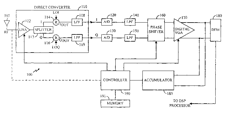
[0020] Fig. 1 illustrates an AMPS receiver system 100 in accordance with an
embodiment of the present invention. The receiver system 100 includes an
antenna
105 for receiving RF forward link signals from various base stations. The
operation
of the antenna 105 is known in the art and need not be described in detail
herein.
The antenna 105 is coupled to a direct converter 110. The direct converter 110
directly converts a radio frequency (RF) signal to a baseband signal without
going
through an intermediate frequency (IF) stage. The forward link signals
received by
CA 02474350 2004-07-22
WO 2004/049580 PCT/US2003/002221
the antenna 105 are RF signals and are converted to baseband signals by the
direct
converter 110. In an embodiment of the present invention, the baseband signals
include zero IF and low IF signals.
[0021] The direct converter 110 includes a low noise amplifier (LNA) 112, a
sputter 113, down-mixers 114 and 116 and filters 118 and 119. The LNA 112
receives the forward link signals from the antenna 105 and amplifies the
forward
link signals. The LNA 112 has a single or multiple gain steps to amplify the
received forward link signals with different gains. The gain of the LNA 112 is
changed by changing the gain from one gain step to another gain step based on
the
strength of the received forward link signal (i.e., the power of the received
forward
link signal), which typically has a range of -25dBm to -125dBm. The strength
(power) of the received forward link signal has a wide range because of
"fading"
such as Rayleigh fading and the variation in the distance from the receiver
system
100 to the base station serving the receiver system 100. The controller 190
selects
the appropriate gain step for the LNA 112, as explained in greater detail
below.
[0022] In the mobile environment, signals are reflected and scattered by
obstacles in their paths including buildings, hillsides, trees, vehicles, etc.
The
scattering of the signals results in multiples copies of the same signal
arriving at the
receiving antenna. These multiple copies, however, take different paths, and
so the
multiple copies arrive at the receiving antenna offset in time. This offset
can cause
the signals to add in a destructive way at one moment and reinforce each other
in the
next moment. This phenomenon is called "fast fading." Thus, fading causes
fluctuation in the strength of the received signals.
[0023] Furthermore, the.rate of fading is related to the wavelength of the ..
received signals and the velocity of a WCD receiving the signals. For example,
a
WCD on a car traveling at 70 m.p.h may experience fading at 200 times per
second.
Therefore, the gain of the LNA 112 needs to be changed at an appropriate rate
to
accommodate the fluctuation of the strength of the received forward link
signals.
[0024] Fig. 3 illustrates the gain steps of the LNA 112. A curve 211 has a
gain of G1, a curve 213 has a gain of G2, and a curve 215 has a gain of G3. In
addition, the LNA 112 may have just an unity gain (i.e., ~H(w)~aB = 0) or may
have a
negative gain (i.e., the input signal is attenuated (e.g., ~H(w)~aB = -20dB)).
Thus, the
CA 02474350 2004-07-22
WO 2004/049580 PCT/US2003/002221
6
gain of the LNA 112 can vary from negative gain to positive gain. For example,
if
the power of a received forward link signal is weak, e.g., -125dBm, the gain
of the
LNA 112 may be increased from G3 to Gl. On the other hand, if the power of a
received forward link signal is strong, e.g., -25dBm, the gain of the LNA 112
may
be decreased from G1 to G2. The LNA 112 may have less or more than the three
gain steps illustrated in Fig. 3, which is used for illustrative purposes. The
gain of
the LNA 112 is controlled by a controller 190 (see Fig. 1), which may be a
processor, a CPU, a DSP processor, a hardware state machine or a micro
controller.
The controller 190 sends a gain control signal to the LNA 112 to change the
gain of
the LNA 112. The operation of the controller 190 will be explained in greater
detail
below.
[0025] When the controller 190 changes the gain of the LNA 112, the LNA
112 also changes the phase of the received forward link signals. In other
words,
when the LNA 112 changes its gain by going to another gain step, the LNA 112
causes a phase shift in the received forward link signals. Thus, the amplified
signal
outputted by the LNA 112 has a phase shift.
[0026] Fig. 2 shows a curve 205 representing an output of the LNA 112. At
a point 206, the controller 190 changes the gain of the LNA 112. As a result
of the
gain change, the LNA 112 causes a sudden phase shift of "0" in the curve 205.
Therefore, instead of following the path traced by a curve 207, the curve 205
follows
a path that has a phase shift of 8. The sudden phase shift in the output of
the LNA
112 may cause certain problems later. However, a phase shifter 160 solves that
problem, as explained in greater detail below.
[0027] As shown in Fig. l, the output of the LNA 112 is coupled to a sputter
113, which splits the output signal into two identical signals for subsequent
quadrature demodulation. The two identical outputs from the splitter 113 are
coupled to identical down-mixers 114 and 116. A conventional down-mixer
receives a radio frequency signal and a local oscillator signal as inputs and
generates
outputs as the sum and difference frequencies of the two input signals. The
down-
mixers 114 and 116 are identical in operation except for the phase of the
local
oscillator. The local oscillator provided to the down-mixer 114 is designated
as a
local oscillator LOI, while the local oscillator provided to the down-mixer
116 is
CA 02474350 2004-07-22
WO 2004/049580 PCT/US2003/002221
7
designated as a local oscillator LOQ. The local oscillators LOI and LOQ have
identical frequency but have a phase offset of 90° with respect to each
other.
Therefore, the output of the down-mixers 114 and 116 are quadrature outputs
designated as IouT and QpUT, respectively. As noted above, the system
illustrated in
the functional block diagram of FIG. 1 uses a direct-to-baseband or a ZIF
architecture. Accordingly, the local oscillators LOI and LOQ are selected to
mix the
RF signal from the LNA 112 directly down to baseband frequency that includes
either zero IF or low IF frequency signals or both.
[0028] The outputs from the down-mixers 114 and 116 are coupled to filters
118 and 119. The filters 118 and 119 are analog low pass filters (LPF) that
select
the desired channel and attenuate out-of-band jammers. The filters 118 and 119
output zero IF or low IF signals.
[0029] The outputs of the filters 118 and 119 are received by analog-to-
digital converters (ADC) 120 and 130, respectively. The ADCs 120 and 130
convert
the received signals to digital form for subsequent processing. The operation
of the
ADCs 120 and 130 are well known in the art and need not be described in any
greater detail herein. Although any type of ADC may be used to implement the
ADCs 120 and 130, the system 100 is ideally suited for operation with high
dynamic
range noise-shaped ADCs, such as a Delta-Sigma ADC, or other noise-shaped
ADCs. Typically, the dynamic range of an ADC is 10*log(maximum signal/noise
of the ADC). The present invention is not limited by the specific form of the
ADCs.
[0031] In an embodiment of the present invention, due to current
consumption constraints, the dynamic range of the ADCs 120 and 130 are limited
to
around 60-75 dB. However, the received forward link signals have a dynamic
range _ ..
of about 100 dB as explained above. Although higher dynamic range ADCs can be
used for ADCs 120 and 130 to accommodate the 100dB dynamic range of the
received forward link signals, the higher dynamic range ADCs increase the
manufacturing cost of the circuit and consume additional battery power.
[0032] As a result of using ADCs having a dynamic range lower than the
dynamic range of the received forward link signals, certain forward link
signals may
saturate the ADCs 120 and 130. Fig. 4 illustrates a curve 220 that represents
the
input voltage of the ADCs 120 and 130. A line 222 represents the upper dynamic
CA 02474350 2004-07-22
WO 2004/049580 PCT/US2003/002221
8
range limit of the ADCs 120 and 130, and a line 224 represents the lower
dynamic
range limit of the ADCs 120 and 130. As discussed above, the range represented
by
the upper limit 222 and the lower limit 224 is less than 100dB. At a point
223, the
input voltage of the ADCs 120 and 130 reaches the upper limit 222, so if the
input
voltage increases above the upper limit 222, the ADCs i20 and 130 will become
saturated.
[0033] Therefore, to prevent such saturation, when the input voltage to the
ADCs 120 and 130 reaches the upper limit 222, the controller 190 sends a gain
control command to the LNA 112 to lower the gain of the LNA 112. The LNA 112
in response to the control command lowers the gain, e.g., from G1 to G2. When
the
gain of the LNA 112 is lowered, the input voltage to the ADCs 120 and 130 is
also
lowered, as shown in Fig. 4 at a point 225. At the point 223, the LNA 112
lowers
the gain step, and the input voltage drops from the voltage at the point 223
to the
voltage at the point 225, thereby preventing the saturation of the ADCs 120
and 130.
On the other hand, if the input voltage drops down to a certain level, the
controller
190 sends a command to the LNA 112 to increase the gain. At a point 226, the
controller 190 sends a command to increase the gain of the LNA 112. Thus, the
input voltage to the ADCs 120 and 130 is increased to the voltage at the point
227.
However, as discussed above, the changing of the gain step in the LNA 112
creates a
sudden change of phase shift in the output of the LNA 112.
[0034] In Fig. 4, the switching point 223 occurs when the input power (i.e.,
the power of the received RF forward link signals) at the antenna 105 is
approximately at -60dBm, and the switching point 226 occurs when the input
power
at the antenna 105 is approximately at -75dBm. ~ However,. in.embodiments of
the
present invention, the switching point 223 may occur when the input power to
the
antenna 105 is above or below -60dBm. Similarly, the switching point 226 may
occur when the input power to the antenna 105 is above or below -75dBm. The
input power points at which the LNA 112 switches the gain step can be
programmed
or changed. For example, the controller 190 may instruct the LNA 112 to lower
the
gain when the input power is at -65dBm and instruct the LNA 112 to increase
the
gain when the input power is at -80dBm as long as such change does not
saturate the
ADCs 120 and 130. In other words, if the input power exceeds a programmable
CA 02474350 2004-07-22
WO 2004/049580 PCT/US2003/002221
9
threshold value, the controller 190 sends a command to the LNA 112 to lower
the
gain, and if the input power dips below a certain programmable threshold
value, the
controller 190 sends a command to the LNA 112 to increase the gain of the LNA
112. The programmable threshold values can be stored in a lookup table in a
memory 191, which is connected to the controller 190. The memory 191 may be
external or internal to the controller 190 and can be a random access memory,
a
read-only memory, EEPROM, a flash memory or any medium used to store the
desired information.
[0035] The instructions for causing the controller 190 to implement the
operational modes described herein may be stored on processor readable media.
By
way of example, and not limitation, processor readable media may comprise
storage
media and/or communication media. Storage media includes volatile and
nonvolatile, removable and fixed media implemented in any method or technology
for storage of information such as processor-readable instructions, data
structures,
program modules, or other data. Storage media may include, but is not limited
to,
random access memory (RAM), read-only memory (ROM), EEPROM, flash
memory, fixed or removable disc media, including optical or magnetic media, or
any
other medium that can be used to store the desired information and that can be
accessed by the controller 190.
[0036] Digital low pass filters 140 and 150 (see Fig. 1) receive the outputs
of
the ADCs 120 and 130, respectively. The filters 140 and 150 attenuate
quantization
noise present in the received signals and perform jammer filtering.
[0037] After the filtering, a phase shifter 160 receives the output of the
filters
140 and 150. The phase shifter 160 may be any ype of phase shifting circuit
that
changes the phase of the received signal such as a cordic rotator. The phase
shifter
160 is not limited to any particular type of phase shifting apparatus. As
discussed
earlier, changing the gain of the LNA 112 changes the phase of the output
signal of
the LNA 112 by "8". In a particular embodiment of the present invention, the
phase
shifter 160 may be a cordic rotator which is a type of digital mixer that
performs
either a dynamic or static phase shift on a signal. In a static phase shift,
the phase
shifter 160 takes the input signal and advances or retards the input signal by
a certain
amount of phase. Basically, the phase shifter 160 removes the phase shift
caused by
CA 02474350 2004-07-22
WO 2004/049580 PCT/US2003/002221
the gain change in the LNA 112. If the gain change causes a phase shift of
"8", the
controller 190 sends a control signal to the phase shifter 160 to impart a
phase shift
of "-A" or approximately "-8" on the phase shifted signal to cancel out the
phase
shift caused by the LNA 112. Thus, when the controller 190 commands the LNA
112 to change the gain step, the controller 190 also sends a command to the
phase
shifter 160 to perform a phase shift to remove the phase shift caused by the
LNA
112. Since the controller 190 knows in advance the amount of the phase shift
change caused by gain step changes, the controller 190 sends a command to the
phase shifter 160 to impart an appropriate amount of phase shift (i.e., a
phase shift
that is approximately equal and opposite to the phase shift caused by the LNA
112)
to the signal received by the phase shifter 160. If the gain in the LNA 112 is
not
changed, the phase shifter 160 does not impart any phase shift to its input
signal. In
other words, the controller 190 does not send any command to the phase shifter
160
to create a phase shift.
[0038] Furthermore, after the controller 190 sends a command to the LNA
112 to change the gain step, the controller 190 waits for a certain time
period before
sending a command to the phase shifter 160 to impart an appropriate phase
shift.
The waiting time period is equal to the signal propagation delay from the LNA
112
to the phase shifter 160. Another term for the propagation delay is group
delay.
Thus, the controller waits for a time period equal to the propagation delay
before
sending out a command to the phase shifter 160 to cause a phase shift so that
the
signal phase shifted by the LNA 112 is given the time to arrive at the phase
shifter
160 before being phase shifted by the phase shifter 160. In other words, the
controller 190 synchronizes the propagation delay from the LNA 112 to the
phase
shifter 160. The actual amount of the propagation delay time is stored in the
memory 191 and is programmable. The removal of the phase shift caused by the
LNA 112 is important for a reason explained in greater detail below.
[0039] Since the AMPS system uses frequency modulation, a forward link
signal can be expressed as follows:
SFM (t) = A~eos 2~z f t + 2~kI f jn(~7)d~7
CA 02474350 2004-07-22
WO 2004/049580 PCT/US2003/002221
11
where A~ = the amplitude of the carrier signal;
f~ = the frequency of the carrier signal;
kf = frequency deviation constant; and
m(t) = the message signal.
[0040] After receiving the forward link signal S~(t), an AMPS receiver
demodulates the forward link signal to retrieve the message signal m(t). A
typical
AMPS receiver in a WCD may have an analog or a digital FM demodulator (DFM)
to demodulate the forward link signal and retrieve the message signal m(t).
The
AMPS receiver system 100 in accordance with an embodiment of the present
invention has a DFM 180 to demodulate the forward link signal. The DFM 180
basically performs an operation equivalent to differentiation (i.e., taking
the time
derivative) of the received forward link signal to demodulate the forward link
signal.
[0041] However, as shown on Fig. 2, the signal 205 outputted by the LNA
112 has a sudden phase shift of 8 at the point 206 because of the gain change
at the
LNA 112. Since the phase was abruptly changed at the point 206, a singularity
point
is created in the derivative at the point 206. As discussed previously, the
DFM 180
performs a differentiation operation to demodulate the received forward link
signals.
When the DFM 180 performs a differentiation operation on a point with abrupt
phase change, such as the point 206, the DFM 180 creates a sudden spike in the
output of the DFM 180. The sudden spike results in a loud "click" noise to the
listener/user of a WCD. Furthermore, if the WCD is traveling at a high speed,
the
rate of fading increases, which results in an increase of the number of
"click" noises.
[0042] Fig. 5 illustrates a curve 230 that represents the output of the DFM
180 for an unmodulated carrier without the removal of the phase shift caused
by the
LNA 112. The curve 230 has a sudden spike at a point 231 that was created by a
differentiation of a singularity point. The spike at the point 231 causes a
"click"
noise to the listener of the WCD. A curve 232 represents the output of the DFM
180 for an unmodulated carrier with the removal of the phase shift caused by
the
LNA 112. The curve 232 does not have any large sudden spikes that may cause
"click" noises since the phase shifter 160 removed any abrupt transition in
phase
caused by the gain step change in the LNA 112.
CA 02474350 2004-07-22
WO 2004/049580 PCT/US2003/002221
12
[0043] Therefore, in order to prevent "click" noises, the phase shifter 160
must remove the phase shift caused by the gain step change in the LNA 112. The
operation of the phase shifter 160 can be expressed mathematically as follows:
l f l cos 8 sin B
LI ~~corrected v LI ~~in
- Sin 9 cOS B
where [I Q]corrected = the output of the phase shifter 160;
[I Q]« = the input of the phase shifter 160.
[0044] In summary, the phase shifter 160 removes the phase shift caused by
the LNA 112 to prevent the creation of "click" noises.
[0045] A digital variable gain amplifier (DVGA) 170 receives the output of
the phase shifter 160. The DVGA 170 amplifies or attenuates the input signal
to a
level proper for the DFM 180, as explained in greater detail below. The DVGA
170
has a control input for receiving control signals from the controller 190 to
control
the gain of the DVGA 170.
[0046] The accumulator 185 receives the output of the DVGA 170 and
calculates the average power of its received input signal over a certain
period of
time. The time period over which the average power is calculated can be easily
determined and implemented by those skilled in the art based on particular
needs
and specifications. In embodiments of the present invention, it is desired to
hold the
calculated average power to be equal to a constant set point.
P = average power = constant set point.
[0047] The controller 190 receives the calculated average power and tries to
maintain the average power to be equal to the constant set point by adjusting
the
gain of the DVGA 170 and the LNA 112. The LNA 112 is used for the coarse
adjustment of the average power, and the DVGA 170 is used for the fine
adjustment
of the average power. The controller 190 sends out respective digital control
signals
to the LNA 112 and the DVGA 170 to control the gain so that the average power
is
maintained at the constant set point.
CA 02474350 2004-07-22
WO 2004/049580 PCT/US2003/002221
13
[0048] The DFM 180 receives the output of the DVGA 170 and demodulates
the input signal to retrieve the message signal m(t) as discussed above. A DSP
processor (not shown) receives the output of the DFM 180 to further filter and
process the output signal of the DFM 180 to produce an audible sound for the
user
of the WCD.
[0049] Fig. 6 illustrates a flow chart outlining a signal processing method
240 in accordance with an embodiment of the present invention. In step 250, a
RF
forward link signal is received. In step 252, the gain of a low noise
amplifier is
adjusted based on the power of the received RF forward link signal. In step
254, the
RF forward link signal is amplified by the low noise amplifier. In step 256,
the
amplified RF forward link signal is converted to a baseband signal. In step
258, the
baseband signal is filtered by an analog filter. In step 260, the baseband
signal is
converted to a digital baseband signal. In step 262, the digital baseband
signal is
filtered by a digital filter. In step 263, it is determined whether the gain
of the low
noise amplifier was changed. If the gain was changed, the control is passed to
step
264, and if the gain was not changed, the control is passed to step 266. In
step 264,
the phase of the digital baseband signal is changed based on the gain change
of the
low noise amplifier. In step 266, the digital baseband signal is amplified by
a digital
amplifier. In step 268, the average power of the amplified digital baseband
signal is
measured. In step 270, the gains of the digital amplifier and the low noise
amplifier
are adjusted based on the average power of the amplified digital baseband
signal. In
step 272, the amplified digital baseband signal is demodulated.
[0050] Fig. 7 illustrates a dual-mode wireless communication device
(DMWCD) 310 in accordance with an embodiment of the present invention. The
DMWCD 310 includes an AMPS receiver 320 and a CDMA receiver 330. The
AMPS receiver 320 and the CDMA receiver 330 share a portion of their circuitry
with each other. The shared circuitry portion is designated as a shaded area
340 in
Fig. 7. The shared portion 340 includes a digital AGC circuit and other
circuitries
that may be shared between the AMPS receiver 320 and the CDMA receiver 330.
In embodiments of the present invention, the shared portion 340 includes the
digital
low pass filters 140, phase shifter 160, digital VGA 170, accumulator 185 and
controller 190 shown on Fig. 1. The digital low pass filters 140, phase
shifter 160,
CA 02474350 2004-07-22
WO 2004/049580 PCT/US2003/002221
14
digital VGA 170, accumulator 185 and controller 190 form a part of the digital
AGC
circuit. The sharing of circuit elements between the AMPS receiver 320 and the
CDMA receiver 330 reduces manufacturing cost and circuit space.
[0051] It is to be understood that even though various embodiments and
advantages of the present invention have been set forth in the foregoing
description,
the above disclosure is illustrative only, and changes may be made in detail,
yet
remain within the broad principles of the invention. Therefore, the present
invention
is to be limited only by the appended claims.