Note: Descriptions are shown in the official language in which they were submitted.
CA 02474444 2006-09-05
METHOD FOR INHIBITING CORROSION OF METAL
FIELD OF THE INVENTION
The present invention relates generally to the process and apparatus for
prevention of oxidation of metal objects in an oxidizing environment. More
particularly,
the present invention relates to apparatus and methods for generating surface
currents
on conducting bodies to inhibit corrosion.
BACKGROUND OF THE INVENTION
In an oxidizing environment, there are substances that under suitable
conditions,
take up electrons and become reduced. These electrons typically come from the
atoms of
metal objects exposed to the oxidizing environment An oxidizing environment is
characterized by the presence of at least one chemical, the atoms of which, in
that
environment, are capable of being reduced by acquiring at least one electron
from the
atoms of the metal. In "donating" an electron, the metal becomes oxidized. As
the
process of oxidation continues, a metal object becomes degraded to the point
that it can
no longer be used for its intended purpose.
On land, oxidation is prevalent in, among other things, bridges and vehicles,
when
they are exposed to salt that is spread on roads to prevent the formation of
ice in cold
climates. The salt melts the snow and ice and, in so doing, forms an aqueous
salt
solution. The iron or steel in the bridges or vehicles, when exposed to the
salt solution, is
readily oxidized. The first visible sign of oxidation is the appearance of
rust on the surface
of the metal object. Continued oxidation leads to the weakening of the
structural integrity
of metal objects. If the oxidation is allowed to continue, the metal object
rusts through and
eventually disintegrates or, in the case of the metal in bridges, becomes too
weak to
sustain the load to which it is subjected. The situation has become worse in
recent years
with increased concentrations of pollutants and the demand for lighter, more
fuel-efficient
vehicles requiring thinner sheet metal and the abandonment of mainframe
construction.
An aqueous salt solution is also the cause of corrosion in a marine
environment
and is responsible for the oxidation of hulls of ships, offshore pipelines,
and drilling and
production platforms used by the oil industry.
- 1 -
CA 02474444 2006-09-05
Early methods of corrosion prevention relied on applying a protective coating,
for
example of paint, to the metal object. This prevents the metal from coming in
contact with the
oxidizing environment and thereby prevents corrosion. Over a long time,
however, the
protective coating wears off and the process of oxidation of the metal can
begin. The only
way to prevent oxidation from starting is to reapply the coating. This can be
an expensive
process in the best of circumstances: it is much easier to thoroughly coat the
parts of an
automobile in a factory, before assembly, than to reapply the coating on an
assembled
automobile. In other circumstances, e.g., on an offshore pipeline, the process
of reapplying a
coating is impossible.
Other methods of prevention of oxidation include cathodic protection systems.
In
these, the metal object to be protected is made the cathode of an electrical
circuit. The metal
object to be protected and an anode are connected to a source of electrical
energy, the
electrical circuit being completed from the anode to the cathode through the
aqueous
solution. The flow of electrons provides the necessary source of electrons to
the substances
in the aqueous solution that normally cause oxidation, thereby reducing the
"donation" of
electrons coming from the atoms of the protected metal (cathode).
The invention of Byrne (U.S. Pat. No. 3,242,064) teaches a cathodic protection
system in which pulses of direct current (DC) are supplied to the metal
surface to be
protected, such as the hull of a ship. The duty cycle of the pulses is changed
in response to
varying conditions of the water surrounding the hull of the ship. The
invention of Kipps (U.S.
Pat. No. 3,692,650) discloses a cathodic protection system applicable to well
casings and
pipelines buried in conductive soils, the inner surfaces of tanks that contain
corrosive
substances and submerged portions of structures. The system uses a short
pulsed DC
voltage and a continuous direct current.
The cathodic protection systems of the prior art are not completely effective
even for
objects or structures immersed in a conductive medium such as sea water. The
reason for
this is that due to local variations in the shape of the structure being
protected and to
concentrations of the oxidizing substances in the aqueous environment, local
"hot spots" of
corrosion develop are not adequately protected and, eventually, cause a
breakdown of the
structure. Cathodic protection systems are of little use in protecting metal
objects that are not
at least partially submerged in a conductive medium, such as sea water or
conductive soil.
As a result, metal girders of bridges and the body of automobiles can not be
effectively
protected by these cathodic systems.
-2-
CA 02474444 2006-09-05
Cowatch (U.S. Pat. No. 4,767,512) teaches a method aimed at preventing
corrosion
of objects that are not submerged in a conductive medium. An electric current
is impressed
into the metal object by treating the metal object as the negative plate of a
capacitor. This is
achieved by a capacitive coupling between the metal object and a means for
providing
pulses of direct current. The metal objeot to be protected and the means for
providing pulses
of direct current have a common ground. In his preferred embodiment, Cowatch
discloses a
device in which a DC voltage of 5,000 to 6,000 volts is applied to the
positive plate of a
capacitor separated from the metal object by a dielectric. Small, high
frequency (1 kilohertz)
pulses of DC voltage are superimposed on the steady DC voltage. Cowatch also
refers to a
puncture voltage of the dielectric material as about 10 kV.
Because of the safety hazards of having the high voltage applied at a place
that
exposes humans and animals to possible contact with the metal object or any
other part of
the capacitive coupling, Cowatch requires limitations on the maximum energy
output of the
invention.
Cowatch discloses a two-stage device for obtaining the pulsed DC voltage. The
first
stage provides outputs of a higher voltage AC and a lower voltage AC. In the
second stage,
the two AC voltages are rectified to give a high voltage DC with a
superimposed DC pulse.
Cowatch uses at least two transformers, one of which may be a push/pull
saturated core
transformer. Because of the use of transformers, the energy losses associated
with the
invention are high. Based on the disclosed values in Cowatch, the efficiency
can be very low
(less than 10%). The high heat dissipation may also require a method of
dissipating the heat.
In addition, the invention requires a separate means for shutting off the
device during
prolonged periods of non-use to avoid discharging the battery.
A somewhat related problem that affects submerged structures is caused by the
growth of organisms. Mussels, for example, are a serious problem with
municipal water
supply systems and power plants. Because of their prolific growth, they clog
the water
intakes required for the proper operation of the water supply system or the
power plant,
causing a reduction in the flow of water. Expensive cleaning operations have
to be carried
out periodically. Barnacles and other organisms are well known for fouling the
hulls of ships
and other submerged parts of structures. Conventional means of dealing with
this include the
use of antifouling paints and thorough cleaning at regular intervals. The
paints may have
undesirable environmental effects while the cleaning is an expensive process,
requiring that
the ship be taken out of commission while the cleaning is done. Neither of
these is effective
in the long run.
-3-
CA 02474444 2006-09-05
It is a goal of the present invention to provide corrosion protection to metal
objects
even when the objects to be protected are not immersed in an electrolyte. It
is a further goal
of the present invention to accomplish this without exposing humans or animals
to the risk of
high voltages. In addition, the device should also be energy efficient,
thereby reducing the
drain on the power source and should not require any special means for heat
dissipation. It
also should, as part of the circuitry, have a battery voltage monitor that
shuts off the pulse
amplifier if the battery voltage drops below a predetermined threshold, thus
conserving
battery power. This is particularly useful because cold weather conditions
under which
corrosion is more likely due to exposure to salt used to melt ice on roadways,
also imposes
greater demands on a battery for starting a vehicle. In addition to cold
weather, high
temperatures and humidity also lead to increased corrosion simultaneously with
increased
demands on battery power for starting a vehicle. It is also a goal of the
present invention to
inhibit the growth of organisms on submerged structures. Finally, it is also a
goal of the
present invention to protect the circuitry from damage if the apparatus is
inadvertently
connected to the battery with reversed polarity.
It is, therefore, desirable to provide an improved control for corrosion
protection.
SUMMARY OF THE INVENTION
It is an object of the present invention to obviate or mitigate at least one
disadvantage
of previous corrosion inhibition methods. In particular, it is an object of
the invention to
provide a method for reducing the rate of corrosion of a metal object.
In a first aspect, the present invention provides a method for reducing a rate
of
oxidation of a metal object. The method includes the steps of generating
electrical
waveforms, coupling the electrical waveforms to the metal object, and inducing
a surface
current over an entire surface of the metal object in response to the
electrical waveforms.
The electrical waveforms have predetermined time-varying characteristics and
are generated
from a DC voltage source, such that each waveform has a temporal AC component.
In an embodiment, of the present aspect, the step of coupling includes driving
the
electrical waveforms through at least two contact points on the metal object,
and the
electrical waveforms can include a resonance frequency of the metal object. In
another
embodiment of the present aspect, the step of coupling can include
capacitively coupling the
electrical waveforms from a first terminal to a second terminal connected to
the metal object,
where the second terminal is connected to a ground terminal of the DC voltage
source.
-4-
CA 02474444 2006-09-05
In yet another embodiment of the present aspect, the step of capacitively
coupling
can include charging a capacitor from the DC voltage source and discharging
stored charge
of the capacitor through the metal object to a ground connection between the
DC voltage
source and the metal object in response to the electrical waveforms. In
alternate aspects of
the present embodiment, the capacitor can be mechanically charged, a first
terminal of the
capacitor can be connected to the metal object and a second terminal of the
capacitor can be
connected to an area of the metal object distant from the ground connection,
and a polarity of
the DC voltage source can be reversed after the stored charge is discharged.
In an alternate embodiment of the present aspect, the step of capacitively
coupling
can include charging a capacitor from the DC voltage source and discharging
stored charge
of the capacitor to a distributed capacitor coupled to the metal object in
response to the
electrical waveforms, where the induced surface current travels in a first
direction in
response to accumulation of stored charge on the distributed capacitor. In an
aspect of the
present embodiment, the step of coupling can include moving a magnetic field
over the metal
object at a frequency corresponding to the predetermined frequency of the
signal pulses.
According to further alternate embodiments of the present aspect, the step of
coupling can include transmitting RF signals corresponding to the electrical
waveforms
through an antenna for receipt by the metal object, the step of generating can
include
generating the electrical waveforms with rise and fall times of about 200
nanoseconds, and
the step of generating can include generating unipolar DC electrical waveforms
or bipolar DC
electrical waveforms.
Other aspects and features of the present invention will become apparent to
those
ordinarily skilled in the art upon review of the following description of
specific embodiments of
the invention in conjunction with the accompanying figures.
BRIEF DESCRIPTION OF THE DRAWINGS
Embodiments of the present invention will now be described, by way of example
only,
with reference to the attached Figures, wherein:
Figs. 1A and 1 B are circuit diagrams of the prior art of Cowatch;
Fig. 2 is a schematic diagram of the apparatus of the present invention;
Figs. 3A, 3B and 3C are circuit diagrams of the preferred embodiments of the
present invention;
Fig. 4 is an alternative embodiment of the present invention;
-5-
CA 02474444 2006-09-05
Fig. 5 is a preferred embodiment of the preferred phase compensation of the
present invention;
Fig. 6 is a circuit for capacitively coupling electrical waveforms to a
metallic
object according to an embodiment of the present invention;
Fig. 7 is a circuit for capacitively coupling electrical waveforms to a
metallic
object according to another embodiment of the present invention; and,
Fig. 8 is a plot of corrosion potential over time for a test panel and a
control
panel.
DETAILED DESCRIPTION
The present invention generally provides a method for reducing the rate of
corrosion
in a metal object by inducing a surface current over the entire surface of the
metal object.
The surface current can be induced by direct or indirect application of
electrical waveforms
having AC components, in response to the electrical waveforms generated from a
circuit.
Electrical waveforms have a time varying component with characteristics such
as frequency
spectrum, repetition rate, rise/fall time, pulses, sinusoids, and combinations
of pulses and
sinusoids. The metal body and the negative terminal of a suitable electrical
source, such as a
DC voltage (battery), are grounded. The positive terminal of the source of DC
voltage is
connected to the electronic circuit that imparts low voltage electrical
waveforms to the
conductive terminal connected to the metal body. The time varying AC
components in the,
electrical waveform responsible for inducing the surface currents are
effective in inhibiting
corrosion, and hence their generation is favoured. Alternate methods of
inducing surface
currents include direct capacitor discharge through the metal body, or
movement of an
electromagnetic field over the metal body, or by generating a signal, with an
appropriate
waveform from an RF source attached to a transmitting antenna such that the
transmitted
signal is received by the metal body.
According to embodiments of the present invention, the generation of
electrical
waveforms having a shape conducive for generating the time varying (AC)
component is
effective for reducing the rate of oxidation. The electrical waveforms may,
but do not
necessarily, include a frequency at which the metal object resonates. It has
been established
that electrical waveforms of a unipolar pulse with a nominal period of 100 uS,
width of 3 uS
and rise and fall times of approximately 200 nanoseconds, are effective at
preventing
corrosion even when an electrolyte is not present. Given that: i) it has been
determined that
the surface currents induced on the metal body by the electrical waveform are
responsible
-6-
CA 02474444 2006-09-05
for the reduction of the rate of corrosion and i) in principle, any electrical
waveform with an
AC component can induce a surface current on a metal object, when properly
coupled to a
metal object. Therefore, it is clear that the possible number of suitable
electrical waveforms
suitable for the reduction of the rate corrosion is virtually infinite. These
surface currents can
be attributed to the skin effect phenomenon, where high frequency electric
current has a
tendency to distribute itself with a higher current density near the surface
of a conductor than
at its core.
The present invention is best understood by first referring to prior art
methods of
preventing oxidation of metal by capacitive coupling. FIG. 1A shows the
circuit diagram of a
push/pull saturated core transformer used in the invention of Cowatch.
Generally, terminal I
is connected to the positive side of the electrical system of a vehicle and
terminal 2 is
connected to the negative side of the electrical system of the vehicle. The
output of the
transformer 81 has three taps, 21, 22 and 23. The tap 21 provides the system
ground, 22
provides 12 volts AC and 23 provides 400 volts AC. The output from the first
stage is fed to
the second stage, a rectifier pulsator, the circuit diagram of which is shown
in FIG. 1 B. The
400 volt AC from 23 is fed to 50, the 12 volt AC from 22 is connected to 51
while the ground
21 is connected to 52. The output of the rectifier pulsator, between 77 and
73, is a 400 volts
DC with 12 volts pulses superimposed on the 400 volts DC.
The specific configuration of the circuits of FIG 1A and FIG 1 B are now
described. In
FIG 1A, terminal I is connected in parallel to core 81 at connection 3,
capacitor 4, and
resistor 5. Resistor 5 is also connected in parallel to transistor 6, diode 7,
capacitor 8, and
resistor 9. Connection 2 to the negative side of the electrical system of the
vehicle, is
connected in parallel to capacitor 4, transistor 6, diode 7, transistor 10,
and diode 11.
Transistor 10 is connected at point 12 (input to the primary winding) to
second winding 14
around saturable ferrite core transformer 81. Transistor 10 is also connected
at point 13 (the
output feedback) to third winding 15 around transformer 81. Capacitor 8 and
resistor 9 are
connected at point 16 (output from feedback) to third winding 15 around
transformer 81.
Transistor 6 is connected at point 17 (input to primary) to first winding 18
around transformer
81. First winding 18 and second winding 14 are each 7 turns of number 20 wire.
Third
winding 15 is 9 turns of number 20 wire. Fourth winding 19 is 225 turns of
number 30 wire,
and fifth winding 20 is 10 turns of number 30 wire.
In FIG 1 B, the 400 volts AC input at point 50 is connected in parallel to
diodes 59 and
60. The 12 volts AC input at point 51 is connected in parallel to diodes 53
and 54. The
system ground input at point 52 is connected in parallel to diodes 55, 56, 57
and 58. Diodes
-7-
CA 02474444 2006-09-05
53, 56, 57 and 60 are connected in parallel to capacitors 61 and 62, resistor
65, SCR 76,
diode 69 and at point 71 to first winding 78 around pulse transformer core 80.
Diodes 54 and
55 are connected in parallel to capacitor 61, resistor 67 and resistor 66.
Resistor 67 is
connected in parallel to capacitor 62 and transistor 75. Resistor 66 is
connected to transistor
75. Transistor 75 is connected in parallel to resistor 65 and SCR 76. Diodes
58 and 59 are
connected in parallel to resistor 68. Resistor 68 is connected in parallel to
SCR 76, diode 69
and capacitor 64. Capacitor 64 is connected at point 72 to first winding 78
around pulse
transformer core 80. Second winding 79 around pulse transformer core 80 is
connected at
point 74 to diode 70. High voltage rectifier diode 70 is connected to output
point 77. The ratio
of the number of turns in the first winding 78 to the number of turns in the
second winding 79
is 1:125, around pulse transformer core 80.
The prior art invention delivers a high voltage DC with low voltage pulses
superimposed on the high voltage DC to a positive plate of a capacitor
connected between
73 and 77. The positive plate of the capacitor is separated from and coupled
to the grounded
metal object by means of a capacitive pad.
FIG. 2 is a functional block diagram illustrating the operation of an
apparatus of the
present invention. The battery 101 is the source of DC power for the
invention. One terminal
of the battery is connected to ground 103. The positive terminal of the
battery is connected to
the reverse voltage protector 105. The reverse voltage protector prevents
application of
reverse battery voltage from being inadvertently applied to the other
circuitry and damaging
the components.
A power conditioner 107 converts the battery voltage to the proper voltage
needed by
the microprocessor 111. In the preferred embodiment, the voltage needed by the
microprocessor is 5.1 volts DC. The battery voltage monitor 109 compares the
battery
voltage with a reference voltage (12 volts DC in the preferred embodiment). If
the battery
voltage is above the reference voltage, then the microprocessor 111 activates
the pulse
amplifier 113 and the power indicator 115. When the pulse amplifier is
activated by a pulse
signal having a positive output of the microprocessor, an amplified pulse
signal having a
positive output is generated by the pulse amplifier and conveyed to the pad
117. The pad
117 is capacitively coupled to the metal object being protected, 119. When the
power
indicator 113 is activated, a power LED in the power indicator is turned on,
serving as an
indicator that the pulse amplifier has been activated. Of course, when the
battery voltage
drops below the reference voltage, all the circuits except the circuit for
detecting the battery
-8-
CA 02474444 2006-09-05
voltage can be turned off to minimize power consumption. The use of the
battery voltage
monitor 109 prevents drain on the battery if the battery voltage is too low.
When the present invention is used to protect a metal object, such as the body
of an
automobile, the pad 117 has a substrate material made of a suitable
dielectric, which in this
case is similar to thin fibre glass and is attached to the object 119 by means
of a high
dielectric strength silicone adhesive. In the preferred embodiment, the
substrate-adhesive
combination has a breakdown potential of at least 10 kilovolts. The adhesive
is preferably a
fast curing one, which will cure sufficiently in 15 minutes to secure the
dielectric material to
the metal object.
With the broad overview of the invention in FIG. 2, the details of the device,
shown in
FIGS. 3A-3C are easier to understand. Nodes numbered 147, 149, 151, 153, 155,
157 and
159 in FIG. 3A are connected to the correspondingly labelled nodes in FIG. 3C.
The unit is
powered from a typical car battery in which the positive terminal of the
battery is connected
to terminal 133 on a connector panel 131. The negative terminal of the battery
is connected
to the body of the car ("ground") and to terminal 137 on the connector panel
131. The pad
117 from FIG. 2 is connected to terminal 139 on the connector panel 131 while
the metal
object 119 being protected in FIG. 2, is connected to the ground. The car
battery, the pad
117 and the metal object 119 being protected and their connections are not
shown in FIG.
3A.
The reverse voltage protection circuit 105 of FIG. 2 comprises of the diodes
D3 and
D4 in FIG. 3A. In the preferred embodiment of the invention, D3 and D4 are
IN4004 diodes.
Those who are familiar with the art will recognize that with the configuration
of the diodes as
shown, the voltage at the point 141 will not be at a significant negative
voltage with respect to
the ground even if the battery is connected to the connector board 131 with
reversed polarity.
This protects the electronic components from damage and is an improvement over
prior art.
As shown in FIG. 3A, a VCC voltage supply is connected to the common terminals
of R1, R2,
Cl, Dl and the VCC input of microprocessor 145.
The power conditioner circuit 107 in FIG. 2, is made of resistor RI, Zener
diode D1
and capacitor C1. These convert the nominal battery voltage of 13.5 volts to
the 5.1 volts
needed by the microprocessor. In the preferred embodiment, RI has a resistance
of 3300,
Cl has a capacitance of 0.1 pF and DI is an IN751 diode. As would be known to
those
familiar with the art, a Zener diode has a highly stable voltage drop for a
very wide range of
currents.
-9-
CA 02474444 2006-09-05
Capacitors C8, C9 and C10 serve the function of filtering the battery voltage
and the
reference voltage. In the preferred embodiment, they each have a value of 0.2
pF. C8 and
C9 could be replaced by a single capacitor with a value of 0.2 pF.
The battery voltage monitor comprises of resistors R2, R3, R4, R5 and R6 and
capacitors C4 and C5. The voltage is monitored by a comparator in the
microprocessor 145.
The voltage divider, comprising of resistors R2 and R3, provides a stable
reference to the pin
P33 of the microprocessor 145. In the preferred embodiment, R2 and R3 each
have a
resistance of 100 Kf2. Accordingly, with the reference voltage of the Zener
diode D1 of 5.1
volts, the voltage at pin P33 of the microprocessor would be 2.55 volts. In
the preferred
embodiment, the microprocessor 145 is a Z86ED4M manufactured by Zilog.
The battery voltage is divided by the resistors R5 and R6 and applied to the
comparator input pins P31 and P32. In the preferred embodiment, R5 has a
resistance of
180K and R6 has a resistance of 100 KU. The comparator in the microprocessor
145
compares the battery voltage divided by R5 and R6, at pins P31 and P32, with
the divided
reference of 2.55 volts at pin P33. Whenever the voltage at pins P31 and P32
drops below
the reference voltage at pin P33, microprocessor senses a low battery voltage
and stops
sending signals to the pulse amplifier (discussed below). The necessity for
connecting pin
P00 to the junction of resistors R5 and R6 through resistor R4 arises because
the
comparator is responsive only to transitions wherein the voltage at pins P31
and P32 drops
below the reference voltage at pin P33. The pin P00 is pulsed approximately
every one
second or so between 0 volts and 5 volts by the microprocessor. When the pin
P00 is at zero
volts, then with a resistance of 100 K0 for resistor R4 in the preferred
embodiment, the
voltage at pins P31 and P32 is below the 2.55 volts reference voltage at pin
P33 when the
battery voltage is below 11.96 volts. When the pin P00 is at 5 volts, the
voltage at P31 and
P32 is above 2.55 volts. By this means, the microprocessor is able to sense a
low battery
voltage in continuous operation. Capacitors C4 and C5 provide AC filtering for
these
voltages.
Those familiar with the art would recognize that the requirement for cycling
pin P00
between two voltage levels, and the requirement for resistor R4, would not be
necessary in
other microprocessors in which the comparator may be responsive to actual
differences
between a reference voltage and a battery voltage, rather than to a transition
of the battery
voltage below the reference voltage.
The use of a microprocessor to generate pulses of DC voltage and the use of a
battery voltage monitor to shut down the apparatus when the battery voltage
drops below a
-10-
CA 02474444 2006-09-05
reference level are improvements over prior art methods. However, those of
skill in the art
will understand that there are well known logic circuits in the art, such as
oscillator/pulse
generator circuits, that can be used to generate the pulses. The Power
Indicator comprises
an LED D2, transistor Q5 and resistors R7, R8 and R9. The transistor Q5 is
driven on by a
positive output of the microprocessor at pin P02. When the transistor Q5 is
on, the LED D2 is
lit. If the battery voltage is reduced to a nominal 12 V, the microprocessor
does not have a
positive output at pin P02 and the LED D2 is turned off. When the battery
voltage rises above
a nominal 12 volts, the microprocessor has a positive output on pin P02 and
the LED D2 is
turned on.
In the preferred embodiment, Q5 is a 2N3904 transistor, R7 has a resistance of
3.9
Ki2, R8 has a resistance of I Kf2 and R9 has a resistance of 10 Kf2.
When the battery voltage is above the nominal 12 V, the microprocessor also
produces an output pulse on pin P20. This is sent to the Pulse Amplifier,
comprising of
resistors R11-R16 and transistors Q1-Q4. In the preferred embodiment, Q1, Q3
and Q5 are
2N3904 transistors, Q2 and Q4 are 2N2907 transistors; R11 has a resistance of
2.7 Kt2, R12
and R13 each have a resistance of 1 Kf2, R14 and R15 have resistances of
390f2, and R16
has a resistance of 1 Kf2. The capacitor C7 provides AC filtering for the
pulse amplifier circuit
and, in the preferred embodiment, has a capacitance of 20 pF. The output of
the pulse
amplifier is applied, through 139 in the connector panel 131, to the coupling
pad 117 that is
attached to the car body. The output has a nominal amplitude of 12 volts.
With the complete absence of any transformers in the invention, high
efficiency can
be readily achieved. This reduces the drain on the battery and is an
improvement over the
prior art. In a presently preferred embodiment, the signal from pin P20 of the
microprocessor
comprises of a pulse with nominal characteristics of a 5 V amplitude, a 3
microsecond width
and a 10 kHz repetition rate. For electrical waveforms of the pulse type, the
rise and fall
times of the amplified pulse signal that is applied to the pad 117 determines
its high
frequency content and hence the temporal variation in the electrical waveform.
In a presently
preferred embodiment, the rise time and the fall times of each pulse that
forms the amplified
pulse signal are about 200ns.
The clock frequency for the microprocessor in the presently preferred
embodiment is
determined by the resonant circuit comprising capacitors C2 and C3 and the
inductor L1.
Use of this circuit is more cost effective than a quartz crystal for
controlling the
microprocessor clock. This is an improvement over the prior art. In the
preferred
embodiment, C2 and C3 have a capacitance of 100 pF while the inductor LI has
an
- 11 -
CA 02474444 2006-09-05
inductance of 8.2 pH. Those familiar with the art would recognize that other
devices or
circuits could be used to provide the timing mechanism of the microprocessor.
Turning now to FIG. 4, an alternative embodiment of the present invention is
illustrated which utilizes an internal capacitor 160, lead 161 and fastener
162 to deliver
pulses to the metal object 119, instead of capacitive pad 117. In FIG. 4, the
output of pulse
amplifier 113 is attached to the positive side of capacitor 160. The negative
side of capacitor
160 is attached to lead 161, which is attached to fastener 162. The output
pulses from pulse
amplifier 113 are thus transmitted to metal object 119 via the path formed by
capacitor 160,
lead 161 and fastener 162, which is attached to metal object 119.
Turning now to FIG. 5 a preferred embodiment of the present invention is shown
illustrating the phase sensor and adjustment circuitry for a system provided
with two or more
electrodes. The present invention provides two or more electrodes for
attachment to large
metallic structures, such as water storage tanks and metallic storage sheds or
large vehicles.
A first and second electrode are attached to the metallic structure or vehicle
being treated so
that the effects of the invention are applied simultaneously at two or more
points. Each of the
electrodes apply a time varying electrical waveform to the object being
treated. A sinusoidal
waveform is an example of a preferred waveform which can be applied, however
any
suitable waveform can be applied with equal effectiveness. A first electrode
on a short cable
is applied at one point on the metal object and a second electrode attached to
a longer cable
is applied at a second point on the metal object being treated. A phase sensor
is used to
adjust the signal so that the impedance difference of the long cable and short
cable does not
affect the phase synchronous relationship of the two applied signals. That is,
the phase
relationship of the signals applied to the metal object and complex impedance
of the first and
second cable is determined and the signal applied to each cable is phase
compensated and
adjusted so that the signals at the distant end of each cable are phase
synchronous or are in
phase when applied to the metal object. A high voltage protection circuit is
provided to
protect the present invention from damage from a high voltage spike or surge.
A variable
speed blinking light emitting diode (LED) is provided to indicate battery
power levels of full,
marginal and low.
As shown in FIG. 5, a first lead 161 and a second lead 166 are driven by pulse
amplifier 213 via signal lines 216 and 214 respectively, in response to the
signal pulses
provided by microprocessor 111. Pulse amplifier 213 contains phase delay
circuitry to adjust
for any phase delay due to impedance differences between cable 161 and cable
166 which
may be of different lengths and thus exhibit different impedances and phase
delays. Different
-12-
CA 02474444 2006-09-05
impedance in each cable tends to independently shift the phase of each output
signal at the
distant end of the cable as applied to the object via fastener 162 or 167.
Thus, the present
invention provides phase compensation, that is, phase sensing of each output
signal at the
fastener or application point to an object and appropriate phase compensation
or delay to
bring each output signal into phase synchronization. Thus, the present
invention monitors
and adjusts the phase of the output signal at each fastener 162 and 167.
Otherwise, the
applied signals can be out of phase syrichronization and cause the application
of the output
signals to be less effective. It is more electrically efficient to adjust the
phase of each fastener
applied signal so that the peak of each fastener signal is coincident with the
peak of other
fastener signals applied to a metal object. Thus, the present invention
insures that each
signal at each fastener applied to a metal object is phase synchronous.
The phase of each signal at each fastener can be determined by attaching each
fastener 162 and 167 to a phase sensor 170 to determine the phase relationship
of each
signal at each fastener 162 and 167, after the signal has passed through the
delivery cables
161 and 166 and capacitors 160 and 165. The microprocessor 111 determines a
phase
difference and sends a phase delay signal to pulse amplifier 213, which
applies a phase
delay signal to pulses sent to each cable so that the signals are in phase
synchronization
when applied to an object through the fasteners. The phase sensor and pulse
amplifier can
also sense and adjust for differences in the complex impedance between two
applied
signals. A similar circuit is used to adjust the phase of applied signals in
the embodiment
where capacitive coupling is used to apply the signals to an object.
Power indicator 215 comprises a voltage sensing circuit, a flasher and a
voltage
indication and LED. The power indicator circuit causes the LED to flash at %
Hertz when the
supply voltage is twelve volts, at % Hertz when the supply voltage is less
than twelve volts
and greater than 11.7 volts, and at'/ Hertz when the supply voltage is less
than 11.7 volts. A
surge protection circuit 172 is provided to protect the present invention from
high voltages
due to regulator failure or other sources of high voltage.
As previously mentioned in the description of the invention shown in FIG. 5,
the
microprocessor 111 can generate an electrical waveform, such as a train of
pulses for
example, for application to the metallic structures. As previously discussed,
an electrical
waveform has a time-varying component and can be of a pulse type or a sinusoid
type, and
have various characteristics such as a specific frequency spectrum, repetition
rate and
rise/fall times. In this present embodiment, the generation or inducement of a
surface current
on the metallic structure is effective for inhibiting corrosion of the
metallic structure. While
-13-
CA 02474444 2006-09-05
surface currents can be generated in response to a time varying electrical
waveform, applied
to the metallic structure, the microprocessor 111 and the pulse amplifier 113
provide unipolar
pulsed DC based signals. However, a Fourier transform of such a signal
indicates that in
addition to a DC component, the signal also includes many AC components.
Generally it has
been observed that the highest frequency components are found to be about
0.35/Trf, where
Trf is the rise/fall time of the pulse, which ever is smaller. While a
unipolar DC signal is used
in the present embodiments, a bipolar DC signal can be used instead with equal
effectiveness. A unipolar signal refers to a signal that makes voltage or
current excursions in
only the positive or the negative direction, while a bipolar signal refers to
a signal that makes
voltage or current excursions in both the negative and positive directions,
such as a
sinusoidal waveform for example.
Those of skill in the art will understand that in the field of digital signal
communications, wires carrying digital signals can exhibit undesired
inductance and
capacitive characteristics. Hence they can behave as a resonant LC circuit
which can cause
undesired transients, and ringing of the signal at the receiving end of the
circuit. At high
transmission speeds where the rise and fall times are very, short this can
pose a serious
problem. While practitioners in the digital signal communications field have
been working
towards minimizing this effect, such transients are preferred for the
embodiments of the
present invention. These transient AC components of the electrical waveforms
of a pulse
type will enhance the frequency component at which the effective LC circuit
oscillates, and
hence enhance surface current generation that reduces the corrosion rate. It
is noted that the
electrical waveforms can have any shape, as long as they possess a time
varying (AC)
component. Naturally, for waveforms of a pulsed type, the microprocessor 111
can be set to
provide the pulse signals at a high frequency, and short rise/fall times, to
generate the time
varying (AC) components. Of course, those of skill in the art will understand
that any suitable
high-speed pulse generation circuit can be used instead of microprocessor 111.
It is noted that surface current generation can be enhanced if the electrical
waveform
contains frequencies at which the metallic object resonates. Since a vehicle
is a complex
electrical structure with respect to AC electrical excitation, it can have an
electrical resonance
at many of the frequencies generated by the electrical waveform. The exact
resonant
frequencies of the vehicle are determined by the structure of the vehicle and
the parasitic
capacitances and inductances present in the electrical circuit and the wires
used to attach
the circuit. Not only will large surface currents result, the surface currents
will radiate
efficiently, turning the metallic object into an effective antenna. Thus, by
selecting the
-14-
CA 02474444 2006-09-05
appropriate waveform shape, and hence frequency spectrum, optimum corrosion
inhibition
can be obtained. However, those of skill in the art will understand that it is
preferable to
control this process in order to avoid RF interference problems.
In an alternate embodiment where high frequency components are not possible,
or
undesired, the high frequency components can be minimized by reducing the
maximum rate
of change present in the electrical waveform. For pulse waveforms this means
the reduction
of the rise and fall times of the pulse. It is noted that low duty cycle pulse
waveforms with
modest rise and fall times are effective for inducing surface currents in the
metal body being
protected. A modest rise and fall time refers to times similar to those
disclosed in the present
embodiments of the invention. In particular, it is noted that the rise and
fall times of
appropriate duration, for a pulsed waveform are primarily responsible for
generation of the
surface currents. Circuit techniques for minimizing signal rise/fall times are
well known to
those of skill in the art.
An alternate technique for generating surface currents in a metallic object is
to
capacitively couple the electrical waveforms directly to the metallic object
to induce surface
current generation. This can be accomplished through direct discharge through
the metal
object or through field induced surface current generation. Following is a
description of
circuits for capacitively coupling electrical waveforms to a metal object
according
embodiments of the present invention.
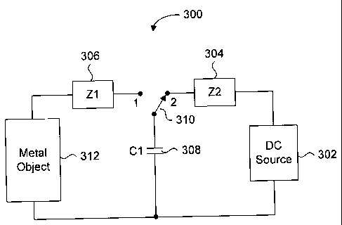
Figure 6 shows a schematic of a circuit for coupling an electrical waveform to
a
metallic object by direct discharge according to an embodiment of the present
invention. The
circuit includes a charge circuit having a DC voltage source for providing a
capacitive
discharge, and a current generation circuit coupled to the metal object for
receiving and
shaping the capacitive discharge from the charge circuit. A terminal of the DC
voltage source
is connected to the metal object, and the current generation circuit applies
the shaped
capacitive discharge to the metal object for inducing a surface current
therein. The capacitive
coupling circuit 300 includes a DC voltage source 302, such as a battery,
impedance devices
304 and 306, capacitor 308, switch 310 and the metallic object 312. In the
present example,
DC voltage source 302, impedance device 304, capacitor 308 and switch 310 form
the
charge circuit for providing the capacitive discharge from capacitor 308 via
switch 310. In
particular, capacitor 308 is arranged in parallel to DC voltage source 302,
and switch 310
couples capacitor 308 to DC voltage source 302 in a charging position for
charging the
capacitor, and to an output in a discharging position for discharging
capacitor 308. In the
present example, the output can be node "1" of switch 310, and the current
generation circuit
-15-
CA 02474444 2006-09-05
includes impedance device 306. Impedance device 304 limits current while
capacitor 308 is
charged, and impedance device 306 is used to shape the current waveform to be
applied to
the metallic object 312. While not shown, voltage source 302 includes a
polarity switch circuit
to reverse its polarity. Switch 310 is controlled to electrically connect the
plate of capacitor
308 to either position 1 or position 2 in Figure 6. Preferably, the two
terminals of capacitor
308 are connected some distance away from each other on the metallic object
312. Those of
skill in the art will understand that the specific type and values of
impedance devices 304,
306, capacitor 308, and voltage source 302 are design parameters. In other
words, their
values are selected to ensure that surface currents effective for reducing the
rate of corrosion
in the metallic object 312 are induced.
In operation, switch 310 is set to position 2 to charge capacitor 308 by
voltage source
302 via impedance device 304. It is assumed in this example that the voltage
source 302
starts with the negative terminal connected to the bottom plate of capacitor
308. Once
charged, switch 310 is toggled to position 1 to discharge the stored charge
through the
metallic object 312 via impedance device 306. Thus, a surface current is
generated through
the metallic object as the positive charge on the top plate of capacitor 308
is discharged
through the metallic object 312. Switch 310 is then toggled back to position 2
and the polarity
of voltage source 302 is reversed via the polarity switch circuit, such that
the bottom plate of
capacitor 308 becomes positively charged. When switch 310 is toggled to
position 1, a
surface current in the opposite direction is generated through the metallic
object 312.
Therefore, charge is applied to and drawn from the metallic object 312 as
switch 310 is
toggled between positions 1 and 2, and the polarity of voltage source 302 is
reversed each
time switch 310 returns to position 2.
Accordingly, the frequency at which capacitor 308 is charged and discharged
can be
controlled by microprocessor 111, and in particular by the electrical waveform
provided by
microprocessor 111. More specifically, switch 310 and the switch circuit of
voltage source
302 can be controlled by the electrical waveform. Therefore, the electrical
waveform is
effectively coupled to the metallic object since the discharge voltage of
capacitor 308
corresponds to an active phase of the electrical waveform. In alternate
embodiments, many
capacitors working in parallel can be selectively connected to the metallic
object to ensure
that surface currents are induced throughout the metallic object 312, and the
capacitor(s) can
be charged mechanically by doing work on the dielectric separating the
capacitor plates.
Furthermore, those of skill in the art will understand that a bipolar voltage
source can be
-16-
CA 02474444 2006-09-05
used instead of the unipolar voltage source 302 described for Figure 6 to
obviate the need
for a polarity switch circuit.
Figure 7 shows a schematic of a circuit for coupling an electrical waveform to
a
metallic object by field induced surface current generation according to an
embodiment of the
present invention. The circuit includes a charge circuit having a DC voltage
source for
providing a capacitive discharge, and a current generation circuit coupled to
the metal object
for receiving and shaping the capacitive discharge from the charge circuit. A
terminal of the
DC voltage source is connected to the metal object, and the current generation
circuit applies
the shaped capacitive discharge to the metal object for inducing a surface
current therein.
Circuit 350 includes the same elements as shown in circuit 300 of Figure 6,
and arranged in
the same configuration, but adds a third impedance device 352, a second switch
354, and a
distributed capacitor plate 356. In the present example, DC voltage source
302, impedance
device 304, capacitor 308 and switch 310 form the charge circuit for providing
the capacitive
discharge from capacitor 308 via switch 310. In particular, capacitor 308 is
arranged in
parallel to DC voltage source 302, and switch 310 couples capacitor 308 to DC
voltage
source 302 in a charging position for charging the capacitor, and to an output
in a
discharging position for discharging capacitor 308. In the present example,
the output can be
node "1" of switch 310. The current generation circuit includes impedance
device 306,
distributed capacitor plate 356, and a discharge circuit including impedance
device 352 and
switch 354. Impedance device 352 shapes the current signal as it is discharged
through
switch 354, and distributed capacitor plate 356 can be many individual
capacitor plates
located at different locations along the metallic object 312. In a variant of
the present
embodiment, each individual capacitor plate forming distributed capacitor
plate 356 can have
its own impedance 352 and switch 354. As in Figure 6, those of skill in the
art will understand
that the specific type and values of impedance devices 304, 306, 352,
capacitor 308, and
voltage source 302 are design parameters selected to ensure effective surface
current
generation. Furthermore, the surface area of each individual capacitor can be
tailored to yield
a desired magnitude of surface current for a specific location on the metallic
object 312.
Tailoring may be required to compensate for the shape of the metallic object
312 and/or
components connected to the metallic object 312, which may affect the
distribution of the
surface current.
In operation, switch 310 is set to position 2 to charge capacitor 308 by
voltage source
302 via impedance device 304, while switch 354 is open. It is assumed in this
example that
the voltage source 302 is configured such that its negative terminal is
connected to the
-17-
CA 02474444 2006-09-05
bottom plate of capacitor 308. With switch 354 open, switch 310 is toggled to
position 1 to
distribute, or share, the stored charge with the distributed capacitor plate
356 via impedance
device 306. Therefore, surface currents are generated through the metallic
object as the
distributed capacitor plate 356 is charged. More specifically, surface
currents flowing in a first
direction are induced as the distributed capacitor plate 356 is charged. With
switch 310 in
position 2, switch 354 is toggled to the closed position to discharge the
distributed capacitor
plate 356 and induce surface currents that flow in a second and opposite
direction.
Accordingly, when switch 310 is in position 2, capacitor 308 begins to charge.
The cycle then
ends by setting switch 354 to the open position.
Accordingly, the frequency at which capacitor 356 is charged and discharged
can be
controlled by microprocessor 111, and in particular by the electrical waveform
provided by
microprocessor 111. More specifically, switches 310 and 354 can be controlled
by the
electrical waveform, to maintain the aforementioned switching operation
sequence.
Therefore, the electrical waveform is effectively coupled to the metallic
object since the
distributed capacitor plate 356 is charged and discharged at a frequency that
is related to the
frequency of the electrical waveform. Those of skill in the art will
understand that
microprocessor 111 can be configured to generate more than one electrical
waveform such
that each electrical waveform controls switches 310 and 354 in the proper
sequence.
An advantage of the present embodiment is the flexibility in customizing
surface
currents at different locations of the metal object by adjusting the values of
the individual
capacitors of the distributed capacitor plate 356, and the values of the
components. Hence,
corrosion reduction throughout the entire surface of the metallic object can
be maximized
regardless of its shape or size.
The previously described techniques for generating a surface current in a
metallic
object require a physical connection between the pulse signal generator
circuit and the
metallic object. A non-contact method for generating a surface current can
involve the
generation of an electromagnetic field to induce a surface current. For
example, a magnetic
field being moved over a metallic surface can induce eddy currents, some of
which would be
surface currents. Such a magnetic field can be provided by a permanent magnet,
which can
be passed over the metallic object surface at a frequency that can be
controlled by the
microprocessor 111. Therefore, the signal pulses are effectively coupled to
the metallic
object since the device generating the magnetic field is moved over a
particular area of the
metallic object in response to an active phase of the signal pulse.
-18-
CA 02474444 2006-09-05
Another non-contact technique for generating a surface current involves
transmitting
a signal with an appropriate shape (waveform) from an RF source through an
antenna such
that the transmitted signal is received by the metallic object. Accordingly,
the signal pulses in
this alternate embodiment can be used to generate the RF signals using well
known RF
circuits, which are then coupled to the metallic object via the transmitted
signals.
Therefore, according to an embodiment of the present invention, the rate of
corrosion
or oxidation of a metal object can be reduced by generating electrical
waveforms with
predetermined characteristics from a suitable waveform generating circuit
powered by a
suitable source of electrical energy, such as a DC voltage source. By coupling
the generated
electrical waveforms to the metal object, surface currents are induced over
the entire surface
of the metal object. While the electrical waveforms are not directly coupled
to the metallic
object in the capacitive coupling and non-contact techniques, they are
considered to be
indirectly coupled to the metal object as they can be used to control other
components for
inducing the surface currents. Those of skill in the art will understand that
the circuit design
and device parameters would be carefully selected to ensure that there is no
interference
with neighbouring systems that may be sensitive to time varying digital
signals.
Because the surface current can be generated with low DC voltage sources, the
embodiments of the present invention can be used in many practical
applications since low
voltage batteries, such as 12 volt DC batteries, are readily available and
more pervasive than
the high voltage sources required in the prior art.
To validate the corrosion inhibition effectiveness of the embodiments of the
present
invention, a corrosion test was conducted upon metal panels prepared for use
as automobile
body panels. A surface current test was conducted upon an automobile to ensure
that
surface currents were present while the apparatus was active to inhibit
corrosion.
The corrosion inhibition effectiveness of the circuit embodiments of the
present
invention, referred to from this point forward as the module, was tested by
scribing the panel
to expose bare metal. The module, being powered by a standard car battery, had
its
terminals connected to the back of the metal panel. This test panel and a
similarly scribed
"control" panel were both continuously sprayed with a salt solution for a
duration of over 500
hours. Electrodes mounted to each panel at the scribe locations monitored the
potential of
each panel over the duration of the test period. A visual inspection clearly
showed that the
test panel had experienced significantly less corrosion than the control
panel, as evidenced
by the lack of rust stains. Furthermore, the potential measurements of each
panel showed
that the test panel eventually attained a potential by about 150mV more
negative than that of
-19-
CA 02474444 2006-09-05
the control panel. The plotted results of the voltage potential (in Volts)
versus time (in hours)
are shown in Figure 8, where the test panel potentials are shown as diamonds
and the
control panel potentials are shown as squares. Therefore, it is concluded that
the more
negative potential of the test panel induced by the embodiments of the present
invention,
contributes to corrosion inhibition.
The surface current test involved connecting the module to an automobile and
measuring the surface currents using well known techniques. In particular, one
terminal of
the module was connected to a drivers side ground bolt of the automobile and
the other
terminal of the module was connected to a fender body panel bolt on the
passenger side of
the automobile. A radio receiver with a calibrated loop current probe was used
to detect and
measure the surface current at different locations of the automobile body. The
test concluded
that surface current was detected over the entire surface of the automobile.
Therefore, the tests confirm that corrosion can be inhibited through the
generation of
surface currents, according to the previously described embodiments of the
present
invention.
While the above-described embodiments of the present invention are effective
for
reducing the rate of corrosion of a metal in the absence of an electrolyte,
they are equally
effective in the presence of an electrolyte. Furthermore, while low voltage DC
voltage
sources have been illustrated in the previously described embodiments of the
present
invention, high voltage DC voltage sources can be used with equal
effectiveness too.
Therefore, the embodiments of the present invention can be applied to large
metal structures
such as sea vessels with metal hulls.
The above-described embodiments of the present invention are intended to be
examples only. Alterations, modifications and variations may be effected to
the particular
embodiments by those of skill in the art without departing from the scope of
the invention,
which is defined solely by the claims appended hereto.
-20-