Note: Descriptions are shown in the official language in which they were submitted.
CA 02474856 2004-08-06
TITIoE OF THE INVENTION
METHOD AND APPARATUS FOR GENERATING A STREAM CIPHER
This application is a divisional of Canadian patent
application Serial No.2,305,264 filed internationally on
May 21, 1998 and entered nationally on April 7, 2000.
BACKGROUND OF THE INVENTION
Field of the Invention
This invention generally relates to secure
~ transmission of digital voice and data communications . More
particularly, the invention relates to a stream cipher with
a plurality of linear feedback shift registers generating
large pseudo-random bit sequences and having multiple
security keys.
Description of the Prior Art
Code division multiple access (CDMA) is a type of
spread-spectrum communication system wherein each
subscriber unit is distinguished from a1.1 other subscriber
units by the possession of a unique code. In order to
communicate with a particular subscriber unit, a
transmitter unit imprints the unique code upon transmission
CA 02474856 2004-08-06
-2-
and the receiver uses the same code to decode the
transmission.
The unique codes used by a CDMA communication system
to transmit voice and data communications appear noise-like
and random. Since the random sequences are generated by
standard deterministic logic elements, the generation of
the bit sequences are predictable and repeatable. It is
the use of these repeatable binary random sequences that
permits easy modulation with any information-bearing
signal. These predictable random sequences are called
pseudo-random sequences.
Each transmitter within a CDMA communication system
includes a stream cipher generator which uses a key to
encipher the voice and data communications . An identical
stream cipher generator at the receiver deciphers the
received enciphered communications using the same key.
As is well known in the prior art, the simplest stream
cipher generator is the linear feedback shift register. A
shift register of a finite bit length is .clocked at a fixed
rate. An exclusive-OR (XOR) gate gene rates the serial
input signal from the XOR combination of some bits of the
shift register. The circuit then proceecLs through a set of
states, eventually repeating itself after a finite number
CA 02474856 2004-08-06
-3-
of clock pulses. However, the stream cipher generated by
linear feedback shift register is related to the length of
the shift register and which bits are combined in the XOR
to generate the next input. If a complex stream cipher is
desired, an expensive shift register having a cumbersome
length must be used.
Zeng et al . , "Pseudo Random Bit Generators in Stream-
Cipher Cryptography", Computer, Vol. 24, No. 2, February 1,
1991, pages 8-17 discloses various circuits using~linear
feedback shift registers for producing stream ciphers. WO-
A-80 02349 discloses a system for encod~_ng and decoding a
dato signal. To encode the data signal, the data signal is
summed with a pseudo random bit sequence. To decode the
encoded data, the encoded data stream is summed with a
pseudo random sequence to recover the data signal.
Accordingly, it is an object of the present invention
to provide a method for generating pseudo-random sequences
with increased complexity.
Accordingly, there is a need for a simple method of
increasing the complexity of stream ciphers to increase security
of enciphered messages.
CA 02474856 2004-08-06
SUN~ARY OF THE INVENTION
A stream cipher generating circuit for use in wireless
communications systems includes at least two mutually coupled
linear feedback shift register (LFSR) circuits, wherein one LFSR
circuit is used to control the clock of the other. This
combination of LFSR circuits generates a stream cipher having a
very large linear complexity and a very large period. The total
output .is balanced with respect to the individual outputs of the
LFSR circuits . The stream cipher generating circuit can be used
in a multiple stage configuration, in which case security is
greatly enhanced since the linear complexity and period of the
stream cipher output increase exponentially.
Other aspects and advantages will become apparent to those
skilled in the art after reading the detailed description of the
preferred embodiments.
BRIEF DESCRIPTION OF THE DRAWINGS
Figure 1 is a block diagram of a conventional spread
spectrum transmitter;
Figure 2 is a block diagram of a conventional spread
spectrum receiver;
Figure 3 is a timing diagram of a pseudo-noise (PN) sequence
used in Figures 1 and 2;
Figure 4 is a diagram showing a conventional cipher stream
generator;
CA 02474856 2004-08-06
-5-
Figure 5 is a block diagram of an embodiment of the spread
spectrum transmitter of the present invention;
Figure 6 is a block diagram of a first embodiment of cipher
stream generator of the present invention;
Figure 7 is a flow chart of the steps for generating a
cipher stream in the first embodiment of the present invention;
Figure 8 is a block diagram of an embodiment of the spread
spectrum receiver of the present invention; and
Figure 9 is a second embodiment of the cipher stream
generator of the present invention.
DESCRIPTION OF THE PREFERRED EN~ODIMENTS
The preferred embodiments are described with reference to
drawing figures wherein like numerals represent like elements
throughout.
A typical prior art spread spectrum transmitter 10, as shown
in Figure 1, includes an analog-to-digital (A/D) converter 12 and
a switch 14. The A/D converter 12 receives an analog vaice
signal, digitizes the signal and outputs the digitized signal to
the switch 14. The switch 14 receives the digital voice signal
from the A/D converter 12 and a digital data signal from a data
terminal (not shown) . It should be readily understood by those
of skill in the art that the data terminal may comprise a
facsimile machine, a computer or any other type of electronic
device that can send or receive digital data. The switch 14
CA 02474856 2004-08-06
-6=
connects the spread spectrum transmitter 10 with an input for
either digital voice data or digital data. The digital voice
data and digital data are hereafter collectively referred to as
digital data.
A mixer 16 combines data from the switch 14 to the cipher
stream generated by the cipher stream generator 17, which has at
least one key 18. After combining the cipher stream to the data,
the mixer 16 outputs the enciphered digital data to a spreader
20, which may be a mixer. A pseudo-random sequence generated by
pseudo-random sequence generator 30 is applied to a first
terminal of the spreader 20. The pseudo-random sequence
generator 30 and the spreader 20 are shown as being contained
within a spread spectrum encoder 40.
The spreader 20 performs a frequency spectrum spreading
function by multiplying the data by the pseudo-random sequence in
the time domain, which is equivalent to convolving the bimodal
spectrum of the data sequence with the approximately rectangular
spectrum of the pseudo-random sequence in the frequency domain.
The output of the spreader 20 is applied to a low-pass filter 50,
whose cutoff frequency is equal to the system chip rate, Fcr:
The output of the low-pass filter 50 'is then applied to one
terminal of a mixer 60 and up-converted, as determined by the
carrier frequency Fc which is applied to its other terminal. The
up-converted signal is then passed through a band-pass filter 70.
CA 02474856 2004-08-06
-7-
The filter 70 has a bandwidth equal to twice the chip rate and a
center frequency equal to the-center frequency of the spread
spectrum system's channel bandwidth. The output of the filter 70
is applied to the input of an RF amplifier 80, .whose_output
drives an antenna 90.
A prior art spread spectrum receiver 100 is shown in Figure
2: An antenna 110 receives the transmitted spread spectrum
signal, which is filtered by a bandpass filter 120. The filter
has a bandwidth equal to twice the chip rate, and a center
frequency equal to the center frequency of the spread spectrum
system's channel bandwidth. The output o:~ the filter 120 is
subsequently down-converted by a mixer,l~t0, possibly in two
stages, to a baseband signal using a local oscillator having a
constant frequency which is approximately the same as the carrier
frequency Fc of the transmitter 10. The output of the mixer 130
is then despread by applying it to a first terminal of the
de spreader 140 while applying the same or similar pseudo-random
sequence as delivered to the spreader 20 to a second terminal of
the despreader 140. The pseudo-random sequence is generated by
20- a despreading code generator 150. The despreader 140 and the
despreading code generator 150 are contained within a spread
spectrum decoder 160 as shown in Figure 2.
More particularly, it will be appreciated that the pseudo-
random sequence used in the receiver 100 o f a spread spectrum
CA 02474856 2004-08-06
_g_
communication system must be synchronized with the pseudo-random
sequence .used in the transmitter 10. The output of the
de spreader 140 is applied to a mixer 170. The decipher stream
generator 172 generates the same cipher ;stream as the cipher
stream generator 17 to decipher the enciphered digital data. In
the prior art, the key 18 used in the transmitter 10 is the same
as the key 174 used in the receiver 100. The receiving key 174
is applied to the cipher stream generator 172 to decipher the
enciphered digital data. The output of the mixer 170 is applied
to a low-pass filter 180, which has a cutoff frequency at the
data rate of the data input to the spread spectrum transmitter
10. The output of the low-pass filter 180 is a replica of the
voice or digital data input as shown in E'igure 1.
A conventional spreading sequence is a pseudo-random digital
sequence as shown in Figure 3. The sequence typically attains
two constant values over time, (+1). The sequence is used to
spread the signal being transmitted and to despread the signal
being received. The stream cipher is generated by a cipher
stream generator 17, as shown in Figure 4. An enciphered data
stream can be deciphered if the key 18 to the original cipher
stream is known and is duplicated at the receiver. The bits are
generated by the cipher stream generator 17 and the data bits are
XOR'ed to encipher the data. The original data stream is
CA 02474856 2004-08-06
-9-
recovered when the enciphered data is XOR' ed with the same cipher
stream as shown by Equation l: '
bimcioci=bi Equation (1)
where bi is the original data stream and ci is the original cipher
stream.
As is well known in the prior art, the simplest cipher
stream generator 17 is the linear feedback shift register 34.
The shift register 34 'comprises a finite number of bits, 33, 35,
37, or finite bit length, which is clocked by a clock circuit 32
at a predetermined fixed rate. A combination of LFSR bits 35, 37
are XOR' ed to generate the next input bit to the LFSR 34 by XOR
gate 38. Coefficients of a primitive polynomial determine which
bits to XOR. An XOR 36 gate combines the output of the LFSR 34
and the digital data stream 39 to encipher the data. The LFSR 34
then goes through a set of states eventually repeating itself
after a finite number of clock pulses supplied by clock circuit
32.
A conventional three b.it LFSR 34 is an example of a cipher
stream generator 17 as shown in Figure 9:. An n-bit shitt
register has a period of 2n-1. Accordingly, far the three bit
shift register 34, the period is seven. Each initial value of
zero or one loaded into each bit of register 34 forms a key,
except for all zeros. For example, if the key is 111, the shift
CA 02474856 2004-08-06
-10-
registex 34 will generate the following values:
Initial loading -~ 111
011
001
100
010
101
110
Repeat ~ 111
011
The three bit LFSR 34, as shown above, has a very small
period (i.e. seven) . Accordingly, a LFSR of this size does not
provide very secure transmission of data..
A spread spectrum transmitter 200 made in accordance with
the present invention is shown in Figure 5. The transmitter 200
includes all of the components of the spread spectrum transmitter
10 shown in Figure 1, which function in the: same manner except
for the cipher stream generator 220 and keys 210 which will be
explained in further detail hereinafter. Although Figure 5 shows
a transmitter 200 for transmitting one channel, multiple channels
may be combined and then enciphered by cipher stream generator
220.
CA 02474856 2004-08-06
-11-
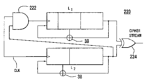
Referring to Figure 6, the cipher stream generator 220
includes twa LFSR circuits, (L~, L2) . The output of the second
LFSR circuit L2 is used to control the clc>ck of the first LFSR
circuit, Ll. For example, the output of the second LFSR L2 is
preferably connected to an AND gate 222, which is connected to
the clock input of the first LFSR Ll. The AND gate 222 could be
replaced by a HAND gate. Other gates such as OR, NOR, XOR, etc.
or a combination of gates may also be used in place of the AND
gate 222. Exclusive-OR gates 38 provide feed back to shift
registers L1, L2. The cipher stream generator 220 also includes
an exclusive-OR gate 224, which is connected to the outputs of
the LFSRs Ll, L2. The exclusive-OR gate 224 combines the outputs
of the LFSRs Ll, L2 and then outputs the cipher stream. The
initial states of the two LFSRs L1, L2 are the two keys that are
shared between the cipher stream generator 220 and decipher
stream generator 320. The decipher stream generator 320, which
will be explained in more detail hereinafter, is preferably the
same as the cipher stream generator 220. The cipher stream
generator 220 and decipher stream generator 320 are preferably
used in synchronous mode (as opposed to self.- synchronous mode)
because the self-synchronous mode is subject to error propagation
due to single bit errors common in wireless transmission. In
self-synchronous stream ciphers, the enciphered digital data is
used as a part of the key for enciphering the following data
CA 02474856 2004-08-06
-12-
bits. The problem with this approach :is that if a bit is
corrupted.during transmission and it is deciphered. incorrectly,
it corrupts the foll owing. bits as well since it is also used as
the cipher key for the following data bits. All ciphering
schemes other than a one time hookup table are periodic. In
order to send a secure transmission, the cipher stream generator
220 and decipher stream generator 320 should have as long a
period as practical. The two LFSRs L1, L2 generate the maximum
period if the tap coefficients of the feedback correspond to a
primitive polynomial. Such a sequence is called a maximum length
sequence (m-sequence).
Although it is not required, in one embodiment, the maximum
period is obtained when the periods of the individual outputs of
the two LFSRs Ll, LZ are relatively prime (the periods of the
individual outputs do not have a common factor) . For example, if
the first LFSR L1 has a bit length of three, the individual
output period is seven. If the second LFSR LZ has a bit length
of two, the individual output period is three. Therefore, the
output periods do not have the same common factor.
A primitive polynomial, which is well known in finite field
algebra, generates a period 2z-1 if it is of. degree L. A set of
polynomials form a finite field. A finite field has at least one
primitive element such that all nonzero elements of the field are
powers of this primitive element.. A polynomial that ha.s a
primitive element as a root is called a primitive polynomial.
CA 02474856 2004-08-06
-13.
Therefore, when the .LFSR circuits L1, ,L2 have lengths LEl and LE2
respectively, the output of both the cipher stream generator 220
and decipher stream generator 320 have the period:
I,EI -j- I,E2
Output period ~2 Equation (2)
When lengths of the two LFSRs ,hl, T~ are in the order of ~20, the
period of the stream cipher is 1012 bits. This means that a 32
kbits/sec data stream can be encrypted continuously for over a
year without repeating the stream cipher.
The linear complexity of the cipher stream generator 220 is
the length of the shortest LFSR that can generate the output of
the cipher stream generator 220. It is often used as a measure
of randomness of the cipher stream generator 220 output. The
linear complexity of this cipher stream generator 220 is in the
order of
Linear complexity -~. (2~E') Le2 f (2~E2) LEx Equatian (3)
If the output of the cipher stream generator 220 were to be
repeated using a single equivalent LFSR, the register would have
to be over 20 million stages long (for LE1 and LE2 ~20 as above) .
A cipher stream generator 220 is called balanced if its
output is the same as the output of each internal LFSR circuit ~1,
Z2 with the same probability. Preferably, the output value should
CA 02474856 2004-08-06
be the same as the output of either one of the ZFSR circuits Zi,
.h2, i . a . a probability of 0 . 5 . It is important to have a cipher
that is balanced because it is easier to break ciphers that are
not balanced. If the combinations of the outputs of the LFSR
circuits Z1, La and the output of the cipher stream generator 220
are considered, it can be seen that the cipher stream is
perfectly balanced and is the same as each Z;FSR ZI, I~ output half
of the time.
The initial state of the cipher stream generator 220 is
determined by the two keys K1 and ICz, which are the initial states
of the twa LFSRs ZI, ZZ respectively. To protect against
insertion attacks, the keys K~ and K2 should be changed often,
(preferably at least once every period of the cipher) . The more
combinations for the keys K1 and K2, the more secure the
transmission. The number of key combinations in this example is
1'EI + ~'E2
Key combinations ~ 2 Equation (4)
which is an extremely large number.
The cipher stream generator 220 of the present invention has
the following advantages: 1) it has a very large linear
complexity: 2) it has a very large periods 3) its output is
balanced with respect to the outputs of the two LFSR circuits L1,
L2; 4) it is implemented with minimal hardwareo and 5) it takes
two keys K1 and K2 which increases its security.
CA 02474856 2004-08-06
-15-
For example, as shown in Figure 6, it is assumed that the
first LFSR circuit Ll has a bit length of 3 and the second LFSR
circuit L2 has a bit length of 2. Further., it is assumed that
key Kl is "111" and key RZ is "11. " The keys Kl and K2 are loaded
into Ll and L2 respectively. Table 1 below provides the states of
the LFSR circuits Li, 7G2; the outputs of the LFSR circuits Ll, L2
and the cipher stream for several consecutivewclock cycles.
Output Output Cipher
Clock L1 Z2 of L1 of L2 Stream
Cycle state state
1 111 11 1 1 0
2 011 O1 - 1 1 0
3 001 10 l 0 1
4 001 11 1 1 0
5 100 01 0 1 1
6 010 10 0 0 1
7 010 12 0 1 1
8 101 01 1 1 0
9 110 10 0 0 1
20 110 11 0 1 1
11 111 01 1 1 0
12 011 10 1 0 1
13 011 I1 1 1 0
14 001 01 1 1 0
15 100 10 0 0 1
16 100 11 0 1 1
17 010 01 0 1 1
18 101 10 1 0 1
19 'l 101 I 11 , 1 ~ 1 0
CA 02474856 2004-08-06
_16_
Output Output Cipher
Clock Ll L2 of L1 of L2 Stream
Cycle state state
20 110 01 0 1 1
21 111 10 ~ 1 ~ 0 1
_ _ _ _ _ _ _ _ _ _ _ _ _ _ _ _ _ - _ - end of one period
22 111 11 1 1 0
23 011 01 1 1 0
24 001 10 1 0 1
25 001 11 1 1 0
a ~ y r ~ ~ n
TABLE 1
From Table 1, the period of the cipher stream is 21 clocks,
which is a multiplication of the individual periods of the LFSR
circuits Ll(7) and Lz(3).
The cipher stream may also be generated using software as
shown in the flow diagram of Figure 7. The initial states, which
are the two keys Kl and K2, are loaded into registers or memory
locations (S1) . If the current output of thE: second LFSR circuit
L2 is ~~1" (S2) , the value of the first LFSR circuit' Ll is updated
(S3), and then the second LFSR circuit L2 is updated (S4).
However, if the current output of LFSR circuit L2 is zero (S2) ,
then the LFSR circuit Ll is not updated and only LFSR circuit L2
is updated (S4) . The outputs of the LFSR circuits Ll, L2 are then
CA 02474856 2004-08-06
-17-
forwarded to an XOR gate, which outputs the cipher stream (S5) .
Steps (S2) through (S5) are then repeated.
A spread spectrum receiver 300 made in accordance with the
present invention as shown in Figure 8 includes all of the
components of the spread spectrum receiver .100 of Figure 2, which
function in the same manner, except for the decipher stream
generator 310 and the keys 320.
The cipher stream generator 220 or the decipher stream
generator 320 can be used in a multiple stage configuration, as
shown in Figure 9, in which case the security is greatly enhanced
since the linear complexity and period increase exponentially.
If LZ~L2~L, then the linear complexity of the multiple stage
configuration with N stages is approximately ~2L2~° and the period
of the output becomes approximately ~22zNw The stream cipher
algorithm explained above can be used in a cascade structure as
in Figure 9 to further increase its security. Each stage may
have the same bit length or the stages may have different bit
lengths. In cascade form, prior stages-generate clocks for the
following stages. As shown in Figure 9, the output of the first
LFSR circuit Ll from stage 1 and the output of the second LFSR
circuit L2 from stage 2 are coupled to an AND gate to form a
digital signal which is, used as the clock for the first LFSR
circuit Ll of stage 2. Similarly, output of the second LFSR
circuit L2 from stage 1 becomes the clock for the second LFSR
CA 02474856 2004-08-06
-18-
circuit L2 of stage 2. More stages can be added in the same
manner. An LFSR is clocked when the signal in its clock input
changes from O to 1. Although the LFSRs LI, L2 at each stage
preferably have the same bit length, they may also be different.
Although the invention has been described by making detailed
reference to certain specific embodiments, such details are
intended to be instructive rather than restrictive.' It will be
appreciated by those skilled in the art that many variations may
be made in a structure and mode of operation without departing
from the scope of this invention as disclosed in the teachings
herein.