Note: Descriptions are shown in the official language in which they were submitted.
CA 02475282 2004-07-16
hoc No: 102-1 CA Patent
VOLUME HOLOGRAM
CROSS-REFERENCE TO RELATED APPLICATIONS
[1] This application claims priority of U.S. Provisional Application No:
60/487,612 filed July
17, 2003, entitled "Thick Volume Hologram for Microwave Frequency Band and
Estimation
of Unreliable Digital Speech Samples via Composite Modelling and Adaptive
Filtering",
which is incorporated herein by reference for all purposes.
FIELD OF THE INVENTION
[2] The present invention generally relates to holographic elements for
modifying
electromagnetic beams, and in particular relates to volume multilayer
artificial dielectric
holograms for modifying microwave beams.
BACKGROUND OF THE INVENTION
[3] Holographic elements have been extensively used in the optical frequency
band for a
variety of applications such as beam switching, beam shaping, data storage,
etc. In a
traditional holographic scheme, an interference of two beams, which are
usually referred to
as a reference beam and an object beam, in a photosensitive film is used to
fabricate a
hologram for applications in the optical frequency band. The interferen<;e
pattern of the two
beams can be imprinted in the photosensitive volume of the film by a post-
processing,
resulting in a modulation of the refractive index in a transverse plane, or in
other words to an
appearance of a grating-like pattern of dielectric perturbations in the film.
A holographic
element fabricated thereby, when illuminated by the reference beam, will
reproduce the
object beam due to diffraction of the former on the grating pattern. In some
applications such
as beam switching or beam shaping the reference beam can therefore be referred
to also as an
input beam, and the object beam - as an output beam.
[4] Holograms are often divided into two categories, depending on a thickness
of the grating
structure and on a beam conversion efficiency defined as a ratio of the output
beam power to
1
CA 02475282 2004-07-16
Doc No: 102-1 CA Patent
the input beam power: thin holograms, having an essentially two-dimensional
(2D) pattern of
dielectric perturbations typically thinner than a wavelength of the input
beam, and thick or
volume holograms, which typically have thickness on the order of the
wavelength or more.
Generally, only a portion of the input beam power is converted to the output
beam power by
a hologram, with the rest being either lost due to material attenuation and
spurious
reflections, or transferred into a set of detrimental side beams formed by
waves diffracted
into lower- and/or higher-order diffraction directions. Thin holograms wherein
every part of
the input beam radiation within its aperture experiences a substantially
single diffraction
event while propagating through the film, have a limited conversion
efficiency, generally not
exceeding 36%, and most of the beam power is lost to the side beams
propagating in other
diffraction orders. Conversely, in thick volume holograms multiple consecutive
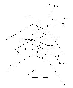
diffraction
events on the dielectric perturbations can theoretically increase the
conversion efficiency to
up to 100%, so that most of the input beam power can be transferred into the
output beam.
Therefore thick volume holograms have a considerable advantage over thin
holograms as
being potentially much more efficient in beam modifying applications.
(5] In a microwave frequency band, sometimes also referred to as a radio-
frequency band
and understood herein as including the cm, mm and sub-mm wavelength range
corresponding to a frequency range 10-1000 GHz, holographic elements for such
applications as beam steering or beam shaping have been exploited to a much
lesser degree
than in optics, mostly due to difficulties of transferring the well-developed
optical
technologies for hologram fabrication into the microwave region.
[6] First, traditional methods of holographic fabrication by imprinting the
interference
pattern of two beams in a photographic material is not easily transferable
into the microwave
frequency band due to a lack of efficient photo-imprinting technologies for
wavelengths
much higher than optical. This difficulty has been overcome in computer-
generated
holograms, wherein a binary or m-ary grating pattern for converting an input
beam into an
output beam is generated by a computer after appropriate diffraction
sinnulations, and then
transferred into either an appropriate surface profile of a dielectric film or
plate for phase
2
CA 02475282 2004-07-16
I~oc No: 102-1 CA Patent
holograms, or into a pattern of opaque obstacles with a spatial period about
or exceeding half
of the beam wavelength for amplitude holograms.
(7] Computer-generated holograms of this type for shaping and re-directing
microwave
beams in the mm and cm wavelength bands were described for example by J.
Meltaus et al.
in an article " Millimeter wave beam shaping using holograms", IEEE
Transactions on
Microwave Theory and techniques, vol. 51, No.4, April 2003. US Patent
5,670,965 to
Tuovinen et al. discloses a compact antenna test range for performing antenna
and radar
cross-section measurements having a transmitter for transmitting an
electromagnetic
wavefront and at least one radio frequency hologram of the aforedescribed type
for receiving
the wavefront, converting the wavefront into a plane wave, and passing on the
plane wave at
an oblique angle with respect to a central axis of the hologram for
illuminating a piece to be
tested.
(8] However, to the best of the inventors' knowledge, no thick volume hologram
for the
microwave frequency band wherein the detrimental side beams are suppressed has
been
disclosed so far. Furthermore, heretofore low loss efficient holograms having
a desirable
thick three-dimensional pattern of dielectric perturbations for the microwave
frequency band
have been difficult to manufacture.
[9] On the other hand, a 3D profiling of the dielectric constant at microwave
frequencies can
be achieved in such materials as artificial dielectrics. An artificial
dielectric can be viewed as
a large-scale model of an actual dielectric, obtained by arranging in a host
dielectric material
a large number of identical conducting or non-conducting inclusions in a
regular or irregular
three-dimensional lattice so that spacing between centers of the inclusions is
much smaller
than a wavelength of microwave field therein. Depending on the spacing of the
inclusions
from each other and on their size, a range of values can be realised for a~,
dielectric
permittivity of the structure, which is different from the dielectric
permittivity of the host
material. Similar to natural dielectrics which owe their higher than unity
refractive index to
an electrical polarisation of its constituent molecules in an external
electric field, the
inclusions in artificial dielectrics give rise to the same effect if their
size and spacing are
3
CA 02475282 2004-07-16
Patent
I~oc No: 102-1 CA
much smaller than the wavelength ~, of the exerted time varying electric
field, typically about
or less than x,/10.
[10] The ability of a dielectric material to be electrically polarized by an
external
electromagnetic field is commonly expressed in terms of relative permittivity,
commonly
defined as a ratio of permittivity of the material to permittivity of free
space. The relative
permittivity is also referred to as a dielectric constant. For purposes of
this application,
permittivity means relative permittivity or the dielectric constant unless
otherwise indicated.
[l l] Artificial dielectrics have been used for fabrication of microwave
lenses, either by
appropriate shaping of the input/output surfaces of a block of an artificial
dielectric as
commonly done in conventional lenses, or by creating a non-homogenous medium
wherein a
3D shaping of the effective dielectric constant, or the effective
permittivity, is obtained by
appropriately varying the size and/or spacing between the inclusions to
achieve a focusing
effect in a flat block of artificial dielectric.
[12] A known method of fabricating an artificial dielectric, wherein a 3D
shaping of the
effective dielectric constant can be conveniently obtained, uses periodic
patterns of metallic
patches printed upon stacked dielectric layers. If a separation between layers
and a size of
metallic print is less than about a tenth of a wavelength of an incident
electromagnetic wave,
dielectric properties of the structure at the wavelength of the incoming wave
can be
characterized by an equivalent dielectric constant whose value can be changed
by varying
geometrical parameters of the structure such as an inter-layer spacing, size
and separation of
the metallic patches.
[13] The aforedescribed layered artificial dielectric materials have been used
for the
manufacturing of flat inhomogeneous microwave lenses, wherein the effective
dielectric
constant is gradually changed on a scale of several wavelengths by a gradual
variation of the
inclusions' size or spatial density, so to produce a focusing effect for an
incident microwave
beam by means of refraction.
4
CA 02475282 2004-07-16
I~oc No: 102-1 CA
Patent
[l4] An object of this invention is to provide a volume hologram having a 3D
lattice of
inclusions arranged to form a volume dielectric grating for modifying an
electromagnetic
beam by diffraction thereupon.
[15] Another object of this invention is to provide a volume hologram
fabricated in an
artificial dielectric comprising a plurality of dielectric sheets with 2D
lattices of inclusions
arranged to form a staked plurality of modulated dielectric layers for
modifying a microwave
beam.
[16] Another object of this invention is to provide a method of fabrication of
volume
holograms for applications in the microwave frequency band using artificial
dielectric
technology.
SUMMARY OF THE INVENTION
[17] In accordance with the invention, a volume hologram for modifying an
input
electromagnetic beam having a wavelength ~, and propagating in an input
direction is
provided comprising a host material having a dielectric constant and a beam
receiving region
for receiving the input electromagnetic beam, a 3D lattice of isolated
inclusions incorporated
in the beam receiving region of the host material, each said inclusion having
a size and a
center, wherein said inclusions are disposed with a characteristic spacing
between centers
thereof about or smaller than one tenth of the wavelength for providing the
volume hologram
with an effective dielectric constant s different from a dielectric constant
of the host material,
and wherein said 3D lattice of inclusions is modulated for inducing a pre-
determined 3D
pattern of dielectric perturbations in the beam receiving region of the host
material, said pre-
determined 3D pattern of dielectric perturbations having multiple regions of
increasing
dielectric constant alternating with regions of decreasing dielectric constant
in a direction
normal to the input direction, for modifying the input electromagnetic beam by
diffraction
thereupon.
5
CA 02475282 2004-07-16
Doc No: 102-1 CA Patent
[18] In accordance with a further aspect of this invention, the host material
of the volume
hologram comprises a plurality of M _> 10 dielectric sheets disposed
sequentially in a first
direction and forming a stacked layered structure crossing the input
direction, wherein each
of the N dielectric sheets incorporates a 2D modulated lattice of the
inclusions with a lattice
period about or less than 0.1~, arranged for inducing a 2D pattern of
dielectric perturbations,
and wherein the M 2D patterns of dielectric perturbations thereby provided
form the pre-
determined 3D pattern of dielectric perturbations.
[19] In accordance with a further aspect of the invention, the volume hologram
is for
modifying at least one of a direction or a shape of a microwave beam having
the wavelength
corresponding to frequency range between lOGHz and 1000GHz.
[20] In accordance with another aspect of the invention, a method of
fabrication of a
volume microwave hologram for modifying a microwave beam is provided, said
method
comprising steps of (a) identifying parameters of input and output microwave
beams, said
parameters including a wavelength, an input direction and an output direction
of the
microwave beam, an input wave front shape and an output wave front shape of
the
microwave beam; (b) identifying a plurality of 2D patterns of dielectric
perturbations and a
spatial separation between said 2D patterns for forming a 3D pattern of
dielectric
perturbations from the plurality of stacked 2D patterns of dielectric
perturbations for
changing at least the direction of the microwave beam from the input direction
to the output
direction by diffraction on the 3D pattern of dielectric perturbations, said
2D patterns of
dielectric perturbations including multiple regions of increasing dielectric
constant
alternating with regions of decreasing dielectric constant in at least one
direction therein; (c)
fabricating a plurality of dielectric sheets, each having a thickness and
comprising a layer of
host material and a 2D lattice of inclusions therein, said inclusions
comprising a conducting
material and having a characteristic spacing between their centers about or
less 1/10 of the
wavelength, wherein the inclusions are arranged to form a 2D pattern of
dielectric
perturbations from the plurality of 2D patterns of dielectric perturbations;
(d) arranging the
plurality of dielectric sheets in a stacked layered arrangement to form a
volume hologram
comprising the 3D pattern of dielectric perturbations.
6
CA 02475282 2004-07-16
Doc No: 102-1 CA Patent
BRIEF DESCRIPTION OF THE DRAWINGS
[21] Exemplary embodiments of the invention will now be described in
conjunction with
the drawings in which:
[22] FIG. 1 is a diagram of a prior art volume hologram.
[23] FIG. 2 is a side view of a volume multilayer artificial dielectric
:hologram in
accordance with an embodiment of the invention.
[24] FIG. 3 is a front view of the volume multilayer artificial dielectric
hologram shown in
FIG.2.
[25] FIG.4 is a plot of dielectric constant of an artificial dielectric.
[26] FIG. 5 is a diagram of a multiplexed volume hologram.
[27] FIG. 6 is an experimental plot of hologram efficiency.
[28] FIG. 7 is an experimental plot of a multiplexed hologram efficiency.
DETAILED DESCRIPTION OF THE PREFERRED EMBODIMENT
[29] In a context of the present invention, a lattice of elements is said: to
be spatially
modulated if one or more of lattice parameters are varied in space in a
periodical or quasi-
periodical manner. The lattice parameters that can be varied include lattice
constant and size
of the constituent elements.
[30] To facilitate a better understanding of the invention, a short overview
of basic
features of volume holograms for changing a characteristic of an
electromagnetic beam will
now be given following an approach and notations of a monograph by Goodman, J.
W.,
"Introduction to Fourier optics", McGraw-Hill, NewYork, 1996, which is
incorporated herein
by reference.
(31) FIG. 1 schematically shows a side view of a volume hologram 5 for
transforming an
input electromagnetic beam 10 impinged upon a beam receiving surface. 15 of
the hologram
into an output electromagnetic beam 20. The act of transforming is understood
herein as an
act of modifying one or several characteristics of the input beam so that a
transmitted or
7
CA 02475282 2004-07-16
Doc No: 102-1 CA Patent
reflected beam has the modified characteristics. A transmission type hologram
is shown as an
example. The electromagnetic beam is approximately monochromatic and has a
spectral
width d~, much smaller than a central wavelength ~, of the beam's spectrum.
The hologram is
formed by a slab of dielectric material transmissive for the input beam and
incorporating a
pre-determined grating-like 3D pattern of dielectric perturbations Os(r) in a
beam receiving
region 40. The pre-determined 3D pattern of dielectric perturbations Bs(r),
where a vector r
denotes a location within the hologram, will also be referred herein as a
dielectric pattern or a
holographic pattern. The dielectric pattern can be designed to modify one or
several
characteristics of the input beam by diffraction upon the pattern, thereby
transforming at least
part of the input beam into the output beam having pre-determined
characteristics. Beam
characteristics that can be modified by a hologram commonly include a
propagation direction
of the beam and a beam shape understood herein as a spatial shape of a
wavefront of the
beam-forming radiation. In some cases, for example when the dielectric pattern
is formed in
a non-linear frequency-doubling material or by a running acoustic wave,
frequency
characteristics of the beam can also be modified.
[32] In accordance with a holographic principle commonly employed in optics,
the
dielectric pattern required for producing a pre-determined output beam upon
illumination of
the hologram by an input beam can be obtained by imprinting an interference
pattern of the
two beams created in the beam receiving region of the dielectric slab into the
dielectric
constant of the slab. The two beams, which are in this context referred to as
an object beam
and a reference beam, are mutually coherent. Denoting an amplitude and a
wavevector of the
input or reference beam at a location r in the beam receiving region of the
hologram as
respectively EI(r) and kl(r) and an amplitude and a wavevector of the output
or object beam
as respectively E2(r) and k2(r), the dielectric pattern formed thereby can be
described by a
proportionality expression (1)
[33] ~E(r) ~ ~E1(r)I2+IE2(r)IZ + ( Ei(r)* E2(r) exp[i(r~~k(r))+i~P] +c.c) (1)
8
CA 02475282 2004-07-16
Poc No: 102-1 CA Patent
[34] wherein a wavevector difference Ok(r) = kl(r)- k~(r), (a,b) denotes a
scalar
multiplication of vectors a and b, cp is a constant wave shift between the two
interfering
waves, and "c.c." denotes a complex conjugate.
[35] With reference to FIG.l, in an illustrative example considered herein the
input and
output beams are plane waves, and the hologram 5 is designed to modify a
propagation
direction of the input beam, transforming the input beam incident on one side
of the
hologram with an incidence angle 8;" into the output beam 20 propagating away
from the
hologram in a direction 21 forming an output angle 8o"t with a direction
normal to an output
surface of the hologram. In a Cartesian coordinate system (x',y',z') having y'
axis directed
in a direction of the wavevector difference ~k, which in this case is
independent on the
location, and axis z' directed normally to a plane of vectors kl,k2, the
dielectric pattern can
be described by a following relationship:
[36] s(r) = Eo + sl(r) cos (Ky
[3TJ where so is an average dielectric constant of the hologram, K = IDkI = A
defines a
spatial period Aof the dielectric pattern, and sl (r) is an amplitude of the
dielectric
perturbations which can slowly vary in space within the beam-receiving region.
The
dielectric pattern has multiple regions of increasing dielectric constant
alternating with
regions of decreasing dielectric constant along a line 111 crossing the beam
receiving region
in the y' direction and can therefore be described as a volume grating with
the grating period
A >_ ~,'/2, which in the case of plane interfering waves described herein is a
one-dimensional
volume grating. If at least one of the input or output beams is not a plane
wave, the dielectric
pattern has a shape of a volume grating which ridges 35 are curved surfaces
defined by
equations (r,~k(r)) = 2~n with integer n. The pattern of dielectric
perturbations will therefore
also referred to herein as a holographic grating.
[38] An important characteristic of a hologram is its efficiency r~, which can
be defined as
a fraction of the input beam power transferred to the pre-defined output beam
by the
holographic grating. It is known in the art that relatively thick gratings
having a grating
9
CA 02475282 2004-07-16
Doc No: 102-1 CA Patent
thickness d > 7~ and operating in a Bragg regime of diffraction are typically
required to
achieve high efficiency, for example above 50%. Such high-efficiency gratings
are referred
to herein us volume or three-dimensional (3D) gratings, and holograms
incorporating such
gratings are referred to herein as volume holograms as opposed to thin
holograms having a
theoretical diffraction limit of 36% which is a maximum of a first order
Bessel function JI(y).
[39] When absorption of the input beam in the hologram material is small, the
efficiency
of the aforedescribed transmission type volume hologram formed by an
interference of two
plane waves can be estimated by using a relationship (3):
[4~] ~-sinz(~ 1+x2/~Z)
1+x2 /~,2
[41] In (3), x and ~ are defined as
_ Sd
[42] x - 2 cos 8 (4)
[43] ~ - Tcnld
~,cos~
[44] where ~ is a mismatch factor, described for example by Goodman, J. W.,
1996,
accounting far possible directional misalignment of the input beam with
respect to the
reference beam used to produce the grating, 8 is an incidence angle of the
input beam within
the hologram satisfying Snell's law
[45] sin(8) = sin(9;n~)/n, n = ~co,
[46] d is the hologram thickness, and nl is a representative of a modulation
of a refractive
index of the hologram corresponding to the modulation of the dielectric
constant of the
hologram:
CA 02475282 2004-07-16
Patent
LZoc No: 102-1 CA
[47] y = s~ (6)
2
[48) A maximum efficiency for a given grating achieved when the mismatch
factor ~ = 0
can be computed from an equation (7)
[49] ~ = sine ~ (7)
[50] It follows from (7) that there is an optimum thickness dopt of the
hologram for which
the efficiency is maximized; this optimum thickness is defined by an equation
- ~ cos(B)
[51] dopt
2n1
[52) The optical technology of the interference pattern imprinting in a photo-
sensitive
material such as photo-refractive glasses (PRG) typically produces relatively
weak gratings
characterized by the refractive index modulation nl ~ 10-2 - 10-4
corresponding to dopt / ?~
50 . . .. 5000. A high-efficiency optical volume hologram can nevertheless be
implemented in
a physically relatively thin slab due to smallness of optical wavelength,
typically on the order
or less than a micron, corresponding to dopt ~ 0.05 ...5 mm.
[53] No similar technology of direct interference pattern imprinting exists
however for the
microwave region of radiation corresponding to frequencies between ~ l OGHz
and ~ lTHz,
where alternative methods of holographic pattern fabrication are required.
These alternative
methods for creating a hologram for microwave radiation should preferably
provide stronger
gratings to realize high holographic efficiency in a physically thin
structure, with dopt
preferably not exceeding several centimeters.
[54] The present invention is directed firstly towards providing an efficient
volume
hologram for modifying a microwave input beam, wherein the 3D holographic
pattern of
11
CA 02475282 2004-07-16
L?oc No: 102-1 CA Patent
dielectric perturbations is formed in a multilayer artificial dielectric.
Another aspect of the
invention is directed towards a method of hologram fabrication enabling the
fabrication of
volume microwave holograms having high efficiency.
[55] An exemplary embodiment of a volume hologram for modifying a
characteristic of an
input microwave beam having a central wavelength ~, is hereafter described
with reference to
FIG. 2 and FIG. 3 respectively depicting side and plane views of a section of
the hologram.
[56] The thick volume hologram 200, disposed to receive an input beam
propagating in an
input direction 201 through a beam receiving surface 204, is formed by M
dielectric sheets
230 disposed in a sequential order one after another in a first direction 203
in a stacked
layered arrangement. FIG. 2 depicts a side view of an illustrative embodiment
of the
hologram in which M = 6; note that M >=10 is normally required to obtain a
high efficiency
hologram. Each dielectric sheet 230 has a plurality of inclusions 210 disposed
on one side
thereof, whereby a 2D lattice of the inclusions is formed on each of the
dielectric sheets. A
set of the M stacked 2D lattices of the inclusions formed on each of the
dielectric sheets
forms a 3D lattice wherein the inclusions are spaced apart from each other,
and wherein a
distance between adjacent inclusions is less than 7~'/3, and preferably less
than x,'/10, where
~,' is a central wavelength of the input beam in the hologram, ~,' _ ~,/n.
7Che set of M
dielectric sheets 230 form a host dielectric material having a layered
structure wherein the 3D
lattice of inclusions 210 is incorporated.
[57) The material, size, and a lattice density of the inclusions, i.e. a
number of inclusions
per unit volume, are selected to affect the dielectric properties of the host
material at the
wavelength of the input beam rather than to cause diffraction or scattering of
the input beam
on individual inclusions. The inclusions 210 are polarized in an electric
field of the input
electromagnetic beam 201 differently than the surrounding host dielectric
material 205;
when a large number of inclusions 210 is present on a scale of one wavelength
~,' of the input
beam in the hologram 200, they provide an average polarization field having an
effect on the
input beam 201 approximately equivalent to changing the dielectric constant of
the medium.
The host dielectric material with a permittivity Eo and the 3D lattice of the
inclusions
12
CA 02475282 2004-07-16
L~oc No: 102-1 CA Patent
incorporated therein form therefore an artificial dielectric having an
effective dielectric
constant sr that can be expressed as a sum of the dielectric constant of the
host material so
and a contribution ~E'(r) from the 3D lattice of inclusions:
$ [rJg] ~r = ~p + DE'(r)
[59] If the 3D lattice is regular and uniform, the contribution 4E'(r) of the
3D lattice of
inclusions into the dielectric constant of the hologram at the wavelength ~,
is approximately
location-independent, provided that the size of the inclusions and the
distance between
centers of the adjacent inclusions is much smaller than 7~'. However if the
size of the
inclusions, the spacing between their centers or their shape is spatially
changing; ~s'(r) can
vary depending on a spatial location r within the hologram. Therefore by
spatially varying or
modulating the shape, size or spacing of the inclusions 210 in the 3D lattice,
a pre-
determined holographic 3D pattern of dielectric perturbations required i:or
modifying the
input beam can be induced. This 3D pattern of dielectric perturbations c;an be
computer-
generated to approximate a holographic 3D pattern that would have been created
by photo-
imprinting a volume interference pattern of the reference and object beams,
and therefore can
be used for modifying characteristics of the input beam in a pre-determined
way.
[60] Although within the scope of present invention the 2D lattices and the 3D
lattice can
be irregular, regular lattices are preferred since it is advantageous to avoid
random spatial
variations of the lattice constant, the size and the shape of the inclusion
which can cause
unwanted scattering of the input beam thereby detrimentally affecting the
efficiency of the
hologram 200.
[61] Different embodiments of the hologram can be envisioned wherein the
inclusions can
have different shape and be either non-conducting with a dielectric constant
different from
the dielectric constant of the host material, or conducting, for example
fabricated from a
metal or a semiconductor. The inclusion can also be in the form of voids in
the host material.
13
CA 02475282 2004-07-16
I~oc No: 102-1 CA Patent
[62] In an exemplary embodiment of the volume hologram schematically shown in
FIG.2
and FIG.3, the inclusions are conducting disks of radius "b" disposed on
sheets of dielectric
material 205 in a regular cubic 2D lattice with a lattice constant "a". A non-
exclusive list of
possible dielectric materials 205 can for example include polymers, ceramics
or composite
materials such as such as Rogers 3003 material commercially produced by Rogers
Corporation commonly used for microwave circuit boards. The dielectric sheets
with the
conducting discs are laminated with a bonding material 215 having a
permittivity close to the
perrnittivity of the dielectric sheets, and bonded to each other to form a
layered structure,
with a distance "c" between the 2D lattices of the metallic disks on adjacent
dielectric sheets
less than ~,'/3 and preferably about or less than x,'/10. The 2D lattice
parameters "a" and "b"
satisfy a condition 2b < a < x,'/10.
[63] The effective permittivity of the artificial dielectric composed of. the
disk inclusions
can be calculated from relations provided by Brown, J., and Jackson, W. in a
paper entitled
"The relative permittivity of tetragonal arrays of perfectly conducting thin
discs", published
in Proc. IEE, paper 17028, Jan.1955:
~ a
[64] sr = so + ~ ~ for c l a >_ 0.6 ( 12)
(1.5(b)3 -0.36)
[65] sr = sa + ~ for c l a <_ 0.6 (13)
1 2(s )
0
(66] where N is a number of disks per unit area, and a is defined as
~csob2 0.441c 2 0.058c3 0.441c
L671 a= 2 ~1- b ~ + g3 Cl+ b ~ . (14).
14
CA 02475282 2004-07-16
Dnc No: 102-1 CA Patent
( 6 8 ] A dependence of the effective permittivity of the multilayered volume
hologram of
the aforedescribed type having c = 0.5 mm, a = 0.6 mm and Eo = 3 on the disk
diameter 2*b
is depicted in FIG. 4. This set of disk and lattice parameters is appropriate
for providing an
artificial dielectric for application in a wavelength range of ~, >_ 1 cm,
corresponding to
frequencies about 30GHz or less. It is evident from FIG.4 that a wide range of
permittivity
values can be realized in this artificial dielectric by changing the disk
diameter. In particular,
by spatially modulating the diameter of disk inclusions in a mufti-layer slab
of the artificial
dielectric, a volume diffraction grating with the refractive index modulation
parameter nl
0.1 or larger can be fabricated, enabling the realization of a high-efficiency
mufti-layer
volume hologram for operation in the microwave frequency range with an optimal
thickness
dopt defined by expression (8) of a few centimeters or less.
[69] Note that the microwave hologram of the present inventions can be
fabricated to
modify not only the input direction, but also other characteristics of the
input beam such as
the shape of the input beam. Fox example, embodiments wherein the 3D
dielectric pattern is
designed to simultaneously re-direct and collimate a diverging microwave beam
can be
realized.
[70] In other embodiments, a multiplexed dielectric pattern can be realized
for
simultaneously modifying characteristics of two or more input microwave beams.
FIG. 5
shows an application of such a hologram, wherein two diverging microwave beams
410 and
420 impinge on the same surface area of a volume microwave hologram 400
incorporating a
multiplexed 3D volume grating pattern induced in the beam receiving region by
an
appropriate modulation of the 3D lattice of inclusions. The hologram
simultaneously
transforms the input beams 4I 0 into a collimated beam 41 S having a direction
different from
the input direction of the beam 410, and transforms the input beams 420 into a
collimated
beam 425 having a direction different from the input direction of the beam
420. The
multiplexed 3D grating pattern can be designed by computer simulations from a
multiplexed
interference pattern of the four beams; and consequently adjusting the pattern
to minimize
cross-coupling between the input/output beam pears.
CA 02475282 2004-07-16
I3,oc No: 102-1 CA Patent
[71] In other embodiments, the volume microwave hologram can be used for beam
splitting and beam combining applications, wherein the 3D pattern is designed
from
multiplexed interference patterns of a single input beam and multiple output
beams, or vice
versa multiple input beams and a single output beam. Generally, embodiments
wherein the
volume microwave hologram of the present invention wherein N input beams are
directed
into M output ports can be envisioned wherein the 3D holographic patterns are
produced by
multiplexing multiple interference patterns.
[72] In other embodiments, the present invention can be used for providing
volume
I O holograms for modifying characteristics of an input electromagnetic beam
having a
wavelength outside of the microwave range. An optic mufti-layer volume
hologram
incorporating a holographic pattern induced by appropriate modulation of a 3D
lattice of
inclusions in accordance with present invention can be envisioned. Such a
hologram can be
realized, for example, using dielectric or semiconductor materials and modern
high-
I S resolution lithographic technologies.
[73] In another aspect of the invention, a method of fabrication of a
multilayer volume
microwave hologram for modifying a microwave beam is provided. The method
includes the
steps of:
[74] I) Identifying target characteristics of the input and output microwave
beams. These
target characteristics include a center wavelength, the input and output
directions of the
microwave beam, an input wave-front shape and an output wave-front shape of
the
microwave beam.
[75] 2) Computing an interference pattern of the input and output microwave
beams and
using it to determine a 3D pattern of dielectric perturbations dE(r) for
transforming the input
microwave beam into the output microwave beam.
[ 7 6 ~ 3) Fabricating a set of M dielectric sheets, each sheet having a 2.D
lattice of closely
spaced inclusions imbedded within or upon it, said inclusions in each sheet
arranged to
I6
CA 02475282 2004-07-16
D,oc No: 102-1 CA Patent
induce the 3D pattern of dielectric perturbations ~s(r) when the dielectric
sheets are
assembled together in a stacked layered arrangement having a pre-determined
spacing
between the adjacent 2D lattices of inclusions.
[77] 4) Bonding the set of M dielectric sheets together one after another in
the stacked
layered arrangement to form a volume mufti-layer hologram comprising the 3D
pattern of
dielectric perturbations.
[78] In the aforedescribed exemplary embodiment shown in FIG. 2,3 wherein the
inclusions are conducting disks supported by dielectric sheets, relationships
(12)-(13) can be
used to compute a 3D pattern of spatial variations of the disk diameter
consisting of M 2D
patterns of spatial variation of the disk diameter required to produce the 3D
pattern of
dielectric perturbations for modifying the input microwave beam. The 3D
pattern of the
dielectric perturbations can be computer-generated using computer simulations
of the
interference pattern of the reference and object beams. The process of
computing the set of M
2D patterns of spatial variations of the disk diameter can include, for
example, the steps of
[79] a) computing an interference pattern of the reference and object beams,
[80] b) determining a starting 3D pattern of dielectric perturbations ~E;~k
approximating the
computed interference pattern, wherein indexes i and~j determine location of a
disk inclusion
in k-th dielectric sheet when the dielectric sheets are assembled in a mufti-
layer hologram, for
a selected lattice period "a" of the disk inclusions and a selected sheet
thickness "c", wherein
both "a" and "c" are less than ~ x,/10,
[81] c) computing a 3D matrix b with elements b;~k specifying disk diameters
for all disk
inclusions of the 3D lattice of inclusions required for inducing the starting
3D pattern of
dielectric perturbations in a mufti-layer structure formed by the assembled
stack of M
dielectric sheets,
[82] d) performing computer simulations of diffraction of the input beam in
the mufti-layer
hologram,
[83] e) if required, optimizing the holographic pattern for example to
increase the
hologram efficiency by iteratively adjusting spatial modulation of the disk
diameter
described by the matrix b;~k and repeating step d).
17
CA 02475282 2004-07-16
I~oc No: 102-1 CA Patent
[84] Diffraction of the input beam in the mufti -layer hologram can be
computed using a
relatively simple method suggested by Alferness, R.in "Analysis of optical
propagation in
thick holographic gratings", Applied Physics, Vol. 7, 1975, pp. 29-33, which
employs a
known transfer matrix representation of a hologram. Following this method,
each dielectric
sheet incorporating a 2D lattice of inclusions can be considered as a thin,
essentially 2D,
grating operating in a Raman-Nath regime of diffraction, which transfer matrix
can be
computed using well-known straightforward methods. A transfer matrix of the
volume
mufti-layer hologram is then computed from the M transfer matrixes of the thin
holograms by
matrix multiplication.
[8S] The aforedescribed method of present invention was verified by
fabricating two
microwave volume holograms for modifying characteristics of microwave beams at
30GHz
frequency, corresponding to ~, = 1 cm in the air.
[86] First, a volume hologram with a single interference pattern designed to
couple an
input plane wave having 0;"~=+55° into a first order transmit mode
having 6°"t=+55°, with a
sign convention as shown in FIG.1.
[87] The hologram was made by laminating 81 layers of Rogers 3003 material of
0.020"
thickness with so =3Ø Arlon CLTE-P bonding material with E = 2.94 was used
to laminate
the layers. Careful consideration was given to the selection of the bonding
material, which
was chosen to minimise a dielectric constant difference between the host
Rogers 3003
material and the bonding film. A metallized side of each layer of the Rogers
3003 material
was patterned and etched to form a pre-determined 2D lattice of conducting
disks. The
volume holographic pattern of dielectric perturbation was designed with the
average
dielectric constant s = 3.6 and E1 = 0.4. The number of layers was chosen so
that the
hologram thickness would be close to an optimum value which was calculated
using
expression (8) to be ~ 4.2 cm.
18
CA 02475282 2004-07-16
r~~c No: 102-i CA Patent
[88] The hologram was measured with a setup composed of two similar microwave
lenses
fed by two horn antennas connected respectively to a microwave source and a
microwave
receiver. By setting the lenses at the proper distance from each other, their
beam waists
coincided with the mid-point of the line that connects the lenses, where the
hologram was
placed. FIG. 5 shows a plot of the measured diffraction efficiency versus
angular orientation
of the receive antenna. It can be seen that about 70% of the power has been
coupled with
high angular selectivity into the transmit output beam propagating away from
the hologram
along 0°"t = 52°. The measured efficiency, although lower than
100%, was considerably
higher than the maximum achievable efficiency of 36% for a thin hologram.
[89] Second, a multiplexed volume hologram was fabricated wherein the 3D
pattern of
dielectric perturbations was designed to change directions of two input beams
as shown in
FIG.4. A method described by Alferness, R., Case, S. K.in "Coupling in doubly
exposed
holographic grating", j. Opt. Soc. Am., Vol. 65(6), 1975, pp. 730-73.9 was
used to design the
multiplexed volume grating for the hologram. A computer code was developed to
determine
design parameters such as so, sl, and d to achieve high coupling between the
reference and
object beam pairs 410, 415 and 420,425 and a low cross coupling between the
two pairs. The
multiplexed hologram was designed to operate at 30 GHz. The volume grating
pattern was
generated from two superimposed incoherent interference patterns corresponding
to two
object and reference beams at 0incl,2 =~ 45° to 0out1,2 =~ 10°.
Index modulation was set at
0.12 for both interference patterns. The structure was composed of 86 layers
of 3003 Rogers
material of Eo=3.0 and 0.15" thickness bonded together by CLTE-P prepreg
material of
so=2.94 and 0.0024" thickness. Two prepreg sheets were used per interface to
keep the
thickness of each layer at a design value of 0.020". FIG. 6 shows measured
angular
distribution of the output beams demonstrating high efficiency and low cross-
coupling
between the beams. The labels "(0,-1) mode" and "(-1,0) mode" refer to output
beams
excited respectively by an input beam having 8inc = -45° and 8inc =
+45° .
(90] The apparatus and method of present invention can be utilized to
translate many
optical applications of volume holograms into the microwave band, including
separation of
two beams having the same frequency and polarization but different angles of
arrival that
19
CA 02475282 2004-07-16
L'n~c No: 102-i CA Patent
proved to be a difficult problem in the microwave band, for beam combining
which translates
into power combining in the microwave band, or for data processing in the
microwave band
similar to holographic data processing in optics.
[91] Of course numerous other embodiments may be envisioned without departing
from
the spirit and scope of the invention.