Note: Descriptions are shown in the official language in which they were submitted.
CA 02475420 2004-08-05
WO 03/067743 PCT/DE02/02563
Title
Circuit arrangement for power factor correction
Technical Field
The present invention relates to a circuit arrangement
for power factor correction.
Power factor correction serves the purpose of reducing
the harmonic content of the input current of a circuit
arrangement. Depending on the power consumption of such
a circuit arrangement, specific requirements apply in
this case. The requirements for ballasts having a power
consumption of more than 25 W are outlined, for
example, in the standard EN 61000-3-2, Part A 14.
Prior Art
A circuit known from the prior art for power factor
correction is described in DE 199 23 238.5.
Further circuit arrangements known from the prior art
for power factor correction serve the purpose of
driving a boost converter having integrated circuits,
of driving a boost converter at a fixed frequency in
intermittent operation using discrete components or of
using a charge pump in the resonant circuit of a
downstream converter without using an upstream
converter for power factor correction.
CA 02475420 2004-08-05
WO 03/067743 - 2 - PCT/DE02/02563
The disadvantage of the circuit arrangements known from
the prior art for power factor correction by means of a
charge pump in the resonant circuit consists in the
fact that they result, in particular in the case of
electronic ballasts having higher ratings, in high
wattless currents in the load circuit. The disadvantage
of the arrangement known from the prior art using
fixed-frequency driving in intermittent operation is
the unfavorable noise spectrum according to EN 55015.
The object of the present invention is therefore to
provide a circuit arrangement for power factor
correction which does not have these disadvantages and,
moreover, can be realized cost-effectively.
Summary of the Invention
This object is achieved according to the invention by a
circuit arrangement for power factor correction having
the features of patent claim 1.
The invention is based on the knowledge that the above-
described object can be achieved by a design using a
self-oscillating boost converter in continuous
operation. Power factor correction is achieved by means
of the constant On time of the central switching
element in the transition mode of operation. The
constant On time and identification of the current zero
crossing in the inductance as is required for operation
in the transition mode is realized with minimum use of
components. The provision of the first capacitor
between the working electrode of the first switching
element and the control electrode of the second
switching element results in both the constant On time
and in the first switching element being switched off
in the zero crossing of the current in the inductance.
At the same time, the first capacitor performs positive
feedback in the switching phases and thus reduces the
switching losses owing to steep switching edges.
CA 02475420 2004-08-05
WO 03/067743 - 2a - PCT/DE02/02563
The solution according to the invention also has the
advantage that, as a result of the continuous operation
and the resulting frequency modulation by the input
voltage, the requirements placed on the components,
including an upstream
CA 02475420 2004-08-05
WO 03/067743 - 3 - PCT/DE02/02563
EMC filter, are minimized. If the circuit arrangement
according to the invention is used for operating a
lamp, in particular in interaction with a cold-start
electronic ballast, the high lamp impedance during the
glow phase in the circuit arrangement according to the
invention does not result in a severe increase in the
intermediate circuit voltage as would be the case,
however, with pump circuits known from the prior art.
The current source, to which the control electrode of
the first switching element is coupled, is preferably
realized either by a second nonreactive resistor, which
is coupled to the first connection terminal of the
input and/or output, or by a separate low-voltage
source having a series resistor.
A limiter network, for example realized by means of a
first zener diode, is preferably connected in parallel
with the first nonreactive resistor and/or the second
switching element such that it can be used to limit the
output voltage. This measure takes into account the
fact that, in the case of the circuit arrangement
according to the invention, during load shedding, for
example during the starting phase or when removing a
connected lamp during operation, the output voltage
rises inversely proportional to the load. The parallel
circuit comprising a first zener diode and the first
nonreactive resistor prevents this by the input power
being controlled downward when the zener voltage of
this first zener diode is reached, to such an extent
that the output voltage of the circuit arrangement
cannot exceed the zener voltage. As an alternative to
this, the output voltage can be limited using a limiter
network in parallel with the second switching element
or oscillation can be completely prevented when an
output threshold voltage is reached.
the' first switching element may comprise an nmos
transistor, and/or the second switching element may
CA 02475420 2004-08-05
WO 03/067743 - 3a - PCT/DE02/02563
comprise an npn transistor. Alternatively, the first
switching element may comprise a pmos transistor,
and/or the second switching element may comprise a pnp
transistor.
The circuit arrangement is preferably designed such
that, during a zero crossing of the current through the
inductance, the first switching element opens. This
measure prescribes a simple condition for starting an
CA 02475420 2004-08-05
WO 03/067743 - 4 - PCT/DE02/02563
oscillation. The zero crossing of the charge current,
which flows through the inductance and the first diode
into the load circuit when the input voltage is
applied, thus causes the circuit to start to oscillate.
A third nonreactive resistor is preferably coupled
between the control electrode of the second switching
element and the first connection terminal of the input.
This additional path increases the length of the On
time in the region of the zero crossing of the input
voltage, which has an advantageous effect on the
harmonic content of the input current.
The series circuit comprising a second diode and a
second zener diode can preferably also be coupled
between the control electrode and the reference
electrode of the second switching element such that the
second zener diode limits the voltage between the
control electrode and the reference electrode of the
second switching element in the reverse direction. The
second diode prevents a current from flowing in the
direction forward of the second zener diode. The
reverse voltage of the zener diode critically
determines the duration of the On time of the first
switching element and thus, at a given load, the level
of the output voltage. If the two diodes are dispensed
with, the reverse voltage is determined by the negative
breakdown voltage of the junction between the control
electrode and the reference electrode of the second
switching element.
Furthermore, the control electrode of the first
switching element and the working electrode of the
second switching element is preferably coupled to the
reference potential by means of a third zener diode,
the third zener diode being arranged such that it can
be used to protect the control electrode of the first
switching element against overvoltages.
CA 02475420 2004-08-05
WO 03/067743 - 4a - PCT/DE02/02563
Further advantageous embodiments are described in the
subclaims.
Brief Description of the Drawings
Exemplary embodiments of the invention will now be
explained in more detail below with reference to the
attached drawings, in which:
CA 02475420 2004-08-05
WO 03/067743 - 5 - PCT/DE02/02563
figure 1 shows a circuit diagram of a first embodiment
of a circuit arrangement according to the
invention;
figure 2 shows a circuit diagram of a second
embodiment of a circuit arrangement according
to the invention;
figure 3 shows a schematic illustration of the time
characteristics of various signals in figures
1 and 2;
figure 4 shows the measured time characteristic of
three signals of a realized exemplary
embodiment;
figure 5 shows the time characteristic, associated
with figure 4, of the input current ie; and
figure 6 shows a circuit diagram of a third embodiment
of a circuit arrangement according to the
invention.
Identical elements and elements having identical
functions in the various exemplary embodiments are
given identical reference numerals throughout in the
text which follows.
Preferred Embodiment of the Invention
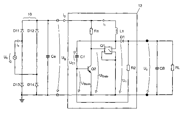
Reference will first be made to the circuit arrangement
according to the invention which is illustrated in
figure 1. Without restricting the possible applications
for the circuit arrangement according to the invention,
it will be described below using the example of an
arrangement for driving an electronic ballast for a
lamp. The associated, basic signal characteristics can
be seen in figure 3.
CA 02475420 2004-08-05
WO 03/067743 - 5a - PCT/DE02/02563
A voltage ue is made available to the circuit
arrangement 12 according to the invention by a voltage
source, in particular a system voltage source. Firstly,
it supplies a current ie to a rectifier network 10,
which comprises four diodes D11, D12, D13, D14. The
voltage ug which is made available
CA 02475420 2004-08-05
WO 03/067743 - 6 - PCT/DE02/02563
at the output of the rectifier network 10 is stabilized
by a capacitor Ce and supplied to the circuit
arrangement 12 according to the invention for power
factor correction.
The capacitor C1 shall be charged at time to to the
negative base/emitter breakdown voltage of the
transistor QZ. The transistor QZ is thus in the off
state, and the transistor Q1 is in the on state via a
pull-up resistor R1, i.e. the voltage ul across the
drain terminal of the transistor Q1 is zero. The
current il through the inductance L1 shall likewise be
equal to zero at time to. The output voltage uZ across
the load RL shall be constant, for example with the aid
of a sufficiently large bulk capacitor CB.
The capacitor C1 is now recharged via R2 during the time
T1 = tl - to, T1 being given by
du~l/T1=1/C1* (uZ/RZ) . (1)
During the time period T1, the current il in the
inductance L1 rises linearly. The gradient of the
current ramp is given by
ll,max/T1 = 1/L1*u9~ (2)
in which ug is the input voltage of the circuit
arrangement according to the invention.
At time tl, the voltage ubase of transistor Qz reaches
the forward voltage and switches the transistor Qz on.
The voltage ugare of transistor Q1 thus becomes zero, and
the transistor T1, for example a MOSFET here, turns
off. At time tl, the current il through the inductance
L1 first commutates onto the capacitor C1 and recharges
said capacitor C1 to the output voltage uZ. Then, the
current il commutates onto the rectifier diode D1 and is
thus supplied to the output circuit. Up to time t2, the
CA 02475420 2004-08-05
WO 03/067743 - 6a - PCT/DE02/02563
current il in the inductance L1 decreases linearly. The
gradient of the negative current ramp can be calculated
from
I-l,max~T2 = l~Ll* (ug-uZ) r
CA 02475420 2004-08-05
WO 03/067743 - 7 - PCT/DE02/02563
in which, disregarding an On time for the transistor
Tl, the following equation applies: T2 = t2 - tl. At
time t2, the current zero crossing in the diode D1 is
reached, see figure 3b), and the diode D1 turns off.
The capacitor C1 is discharged by means of the
inductance L1 and in this manner depletes the base of
the transistor Q2. The transistor QZ thus turns off, and
the voltage ugate across the gate of the transistor Q1 is
pulled up by means of the pull-up resistor R1. Q1 thus
turns on and pulls the voltage ul across its drain to
zero. The capacitor C1 is discharged by means of the
drain/source junction of the transistor Q1 up to the
negative base/emitter breakdown voltage of the
transistor Q2. This positive feedback makes it possible
for the transistor Q1 to switch off rapidly, and thus
minimizes the switching losses. The state at time to is
thus reached, and the cycle begins from the beginning.
The circuit arrangement according to the invention
provides for the time T1 = tl-to to be constant
independently of the input voltage u9 and thus
independently of the voltage ue. It can be seen
directly from equation (2) that in this case il,max is
proportional to the input voltage ug. Furthermore, the
rms value of the current il is equal to the active
component of the input current ig. In continuous
operation, the peak value for the current il in the
inductance L1 is proportional to the input current ig
according to the equation
ll,max = ~ * 1g
The circuit principle in which the transistor Q1 is
opened again at the zero crossing of the current il at
time t2 prescribes continuous operation. The condition
for power factor correction is as follows:
(5)
ue "' le
CA 02475420 2004-08-05
WO 03/067743 - 7a - PCT/DE02/02563
and, from (3) and (4) where ug = luel and ig = lief , is
thus met by the circuit arrangement according to the
invention.
To start the oscillation:
CA 02475420 2004-08-05
WO 03/067743 - 8 - PCT/DE02/02563
Once a voltage ug has been applied, the capacitor C1 is
charged by means of the inductance L1 and the diode D1.
The base of the transistor Q2 is driven via the
resistor RZ whilst the output voltage uZ is built up,
as a result of which the transistor QZ turns on. The
voltage ugate across the gate of the transistor Q1 is
thus equal to zero and in this phase turns the
transistor Q1 off.
Once the capacitor C1 has been recharged when the first
voltage peak value for the input voltage has been
reached, the current il through the inductance L1 passes
through zero. As has already been explained above, this
results in the capacitor C1 being recharged and a cycle
starting, as shown in figure 3. The circuit arrangement
according to the invention thus begins to oscillate
automatically once the input voltage has been applied.
With reference to the embodiment illustrated in figure
2 of a circuit arrangement according to the invention,
further refinements of the circuit principle according
to the invention are described below: the time TZ
decreases inversely proportionally to the increasing
output voltage uZ. The input power is thus pulled back
as the output voltage uZ increases, which is
advantageous for the circuit arrangement. In order to
completely adjust the output voltage uZ in the case of
a resistive load, the input power would need, however,
to be pulled back in proportion to the square of the
output voltage uz. This means that the output voltage uZ
during load shedding, for example during the starting
phase of a lamp or when removing a lamp during
operation, nevertheless increases inversely
proportionally to the load. In order to prevent this, a
zener diode D4 can be introduced. Said zener diode DQ is
in parallel with the nonreactive resistor R2 and limits
the output voltage uZ by the time T1 and thus the input
pourer being controlled downward when the zener voltage
across the zener diode D4 is reached, to such an extent
CA 02475420 2004-08-05
WO 03/067743 - 8a - PCT/DE02/02563
that the output voltage uz cannot exceed the zener
voltage of the diode D4,
A nonreactive resistor R3 is coupled between the
control electrode of the second transistor QZ and the
first connection terminal of the input. This resistor
can be used to further reduce the harmonic content of
the input current, since the converter cannot otherwise
transmit any power in the region of the zero crossing
of the input voltage when On times are too short.
CA 02475420 2004-08-05 I
WO 03/067743 - 9 - PCT/DE02/02563
Continuous operation of the circuit arrangement
according to the invention is used to limit the current
amplitude of the current il t0 ll,max ~*Ig . This reduces
the requirements in terms of components, in particular
for saturation of the inductance L1.
The switching frequency f in the circuit arrangement
according to the invention is f = 1/(T1+TZ). Since,
according to equation (3), TZ is dependent on the input
voltage ug, the spectrum of the conducted, emitted
noise during operation using the system voltage ue is
smoothed. The lowest frequency is reached at high input
voltages ug. Since at high input voltages the highest
currents il in the inductance L1 need to be
disconnected, the circuit can be dimensioned such that,
below the step change in the evaluation curve, this
frequency is 50 kHz.
According to equation (1), the capacitor C1, together
with the nonreactive resistor RZ, determines the time
constant T1. The capacitor C1, however, has even further
advantageous functions in the circuit arrangement
according to the invention:
- The capacitor C1 makes it possible to rapidly
deplete the base of the transistor QZ at time t2 by
means of positive feedback in the switching phase.
Conversely, at time tl, the capacitor C1 assists,
likewise by means of the effect of positive
feedback, in switching the transistor QZ on and
thus in a ~~hard" turn-off of the transistor Q1.
Depending on the dimensions, it may be necessary
to protect the base of the transistor QZ against
overcurrent when the capacitor C1 is recharged, by
means of two diodes DZa, DZb, see figure 2, in
parallel with the base/emitter path of the
transistor Q2. The zener diode DZb limits the
CA 02475420 2004-08-05
WO 03/067743 - 9a - PCT/DE02/02563
negative base/emitter voltage of the transistor
Q2. The time T1 is thus independent of component
scatter and temperature behavior of the breakdown
voltage of the transistor Q2.
- The capacitor C1 limits the edge steepness when
the polarity of the voltage across the inductance
L1 is reversed.
CA 02475420 2004-08-05
WO 03/067743 - 10 - PCT/DE02/02563
The transistor QZ advantageously clamps the gate of the
transistor Q1 "hard" at zero volts. This is necessary
for recharging the gate capacitance of the transistor
Q1 rapidly and for causing the transistor Q1 to turn off
rapidly. In addition, the switching losses in the
transistor Q1 can thus be kept low. Conversely, the
transistor Q1 is switched on by means of the pull-up
resistor R1. This may take place "softly", since the
current il in the inductance L1 at this time must first
be built up starting from zero.
In order to protect the gate in this circuit against
overvoltages, a zener diode D3, see figure 2, can be
connected between the gate terminal and the reference
potential for the transistor Q1.
In one advantageous development of the invention, the
pull-up resistor R1 is connected to an internal
low-voltage supply. The zener diode D3 may thus be
dispensed with. Furthermore, this measure makes it
possible to dispense with the high voltage requirements
for the resistor R1.
Figure 4 shows the time characteristic of the output
voltage uZ of the current il and of the voltage uba5e
across the base of the transistor Q2 over time using an
experimental design for a circuit arrangement according
to the invention. The voltage peaks in the
characteristics for the voltages uZ and ubase result from
the recharge currents of the capacitor C1 and lead to
losses in the transistor Q2, as long as they are not
derived using optionally inserted diodes DZa and Dzb.
Figure 5 shows the time characteristic of the input
current ie when driving using a sinusoidal system
voltage ue. In the region of the zero crossing of the
system voltage ue, the voltage across the inductance L1
rio Jlonger reaches the output voltage uZ. Power transfer
is thus not possible in this region for a very short
CA 02475420 2004-08-05
WO 03/067743 - 10a - PCT/DE02/02563
period of time. These current distortions result in a
harmonic content which can be tolerated depending on
requirements. The additionally introduced third
resistor R3 between the base of the transistor QZ and
the rectified input voltage can be used to largely
compensate for this effect.
CA 02475420 2004-08-05
WO 03/067743 - 11 - PCT/DE02/02563
Figure 6 shows a further exemplary embodiment of the
invention. In contrast to figure 2, a second capacitor
C2 is connected between the control electrode and the
reference electrode of the second switching element Q2.
In addition, the reference electrode of the second
switching element Q2 is connected to the reference
potential via a fourth resistor R4. The second
capacitor C2 eliminates one disadvantage which arises
owing to the multiple function of the first capacitor
Cl. Firstly, the value of the first capacitor Cl
determines the On time T1 of the first switching
element Ql, and secondly the first capacitor C1
represents the positive feedback which maintains the
oscillation of the entire circuit arrangement. In
practice, changes in the voltage of several hundred
volts occur across-the first capacitor C1. As well as
the desired value for the first capacitor C1,
undesirably high charge and discharge currents result
which entail high component loads. According to the
invention, the second capacitor cancels out the
multiple function of the first capacitor Cl. The value
for the second capacitor C2 is selected such that it
essentially determines the On time T1 of the first
switching element Q1. The value for the first capacitor
C1 can then be selected to be so small that only its
positive feedback function is maintained. The
abovementioned charge and discharge currents can thus
be reduced. The value for the fourth resistor R4
represents a further possible way of influencing both
the positive feedback function of the first capacitor
C1 and the On time T1 of the first switching element
Ql. Fine tuning is thus possible. The value for the
fourth resistor R4 may also be zero, however.
In summary, the circuit arrangement according to the
invention results in particular in the following
advantages:
CA 02475420 2004-08-05
T~TO 03/067743 - 11a - PCT/DE02/02563
- depletion, by virtue of the principle, of the
transistors, brought about by the positive
feedback by means of the capacitor C1 when the
transistor Q1 turns off, makes possible low-loss
switching of high currents;
- the capacitor CI or the capacitors C1 and C2 are
responsible for dimensioning of the time T1 and at
the same time cause the transistor Q1 to turn off
in the zero crossing of the current il in the
inductance L1;
CA 02475420 2004-08-05
WO 03/067743 - 12 - PCT/DE02/02563
- the capacitor C1 or the capacitors C1 and CZ make
possible a "soft" commutation of the current il at
time tl;
- the variation in the output voltage uZ as a result
of a variation in the load is partially, i.e.
linearly instead of quadratically, adjusted by the
dependence of the time T1 on the output voltage uZ.