Note: Descriptions are shown in the official language in which they were submitted.
CA 02475974 2004-08-11
WO 03/069865 PCT/US03/04384
FREQUENCY TIMING CONTROL LOOP FOR WIRELESS
COMMUNICATION SYSTEMS
BACKGROUND
Field
[1001] The present invention relates generally to data communication, and more
specifically to a frequency-timing control loop for wireless (e.g., CDMA)
communication
systems.
Background
[1002] In a wireless communication system, an RF modulated signal transmitted
from
a source may reach a receiver at the destination, via a number of propagation
paths (e.g., a
line-of-sight path and/or reflected/scattered paths). In a multipath
environment, the signal
at a given receiver may thus include a number of instances of the transmitted
signal. Each
signal instance (or multipath component) may be associated with a different
Doppler
frequency shift due to movement of the receiver (or more precisely, due to
relative motion
between the receiver and the transmitter/reflector/scatterer associated with
the signal
instance). Each signal instance may further be associated with a different
arrival time
determined by the propagation path.
[1003] At the receiver, the received signal is conditioned and digitized to
provide data
samples. Conventionally, a rake receiver is used to process the data samples
for multiple
signal instances in the received signal. The rake receiver includes a number
of finger
processors, each of which may be assigned to process a respective signal
instance based
on the data samples. Each finger processor may include a rotator and an
interpolator used
to respectively provide frequency and time tracking for the assigned signal
instance. In
particular, the frequency error of the signal instance may be estimated with a
frequency
control loop and the rotator may then be used to remove this estimated
frequency error
from the data samples to provide frequency-translated data samples. Similarly,
the timing
error of the signal instance may be estimated with a timing control loop and
the
interpolator may then be used to re-sample the frequency-translated data
samples at the
optimal or near-optimal sample timing for the signal instance (i.e., the
sample timing
associated with the highest signal-to-interference-and-noise ratio (SINR) for
the signal
CA 02475974 2011-07-29
74769-936
2
instance) to provide on-time samples. The on-time samples within each finger
processor would then have the frequency and timing errors associated with the
assigned signal instance removed.
[1004] The use of separate frequency and timing control loops to individually
track the frequency and timing of a given signal instance provides good
performance
when the SINR of the received signal is low (such as for an IS-95 CDMA
system).
When such is the case, the SINR of the processed data samples (i.e., after
rotation
and interpolation) is not quite as sensitive to the rotation and interpolation
of the data
samples to remove the frequency and timing errors. However, for a system
designed
to operate at high SINRs (such as for an IS-856 CDMA system), the rotation
and/or
interpolation may result in noticeable degradation in the SINR of the
processed data
samples, which may then degrade performance.
[1005] There is therefore a need in the art for techniques to acquire and
track
the frequency and timing of a given signal instance, that are optimized for
high SINR
operating environments.
SUMMARY
[1006] Techniques are provided herein to acquire and track both the frequency
and timing of a given signal instance such that re-sampling is not needed for
the
signal instance. This may then provide improved performance, especially at
high
SINR operating environments.
[1006a] According to one aspect of the present invention, there is provided a
frequency-timing control loop comprising: a timing control loop operative to
process
data samples for a received signal to derive a first control indicative of
timing error in
the data samples for a particular signal instance in the received signal; and
a
frequency control loop coupled to the timing control loop and including a
frequency
discriminator operative to derive a second control indicative of frequency
error in the
data samples for the signal instance, and a first loop filter operative to
filter the first
CA 02475974 2011-07-29
74769-936
2a
and second controls to provide a third control for adjusting frequency and
phase of a
periodic signal used to process the received signal to provide the data
samples.
[1006b] According to another aspect of the present invention, there is
provided
in a wireless communication system, a method of acquiring and tracking
frequency
and timing of a signal instance in a received signal, comprising: first
processing data
samples for the received signal to provide a first control indicative of
timing error in
the data samples for the signal instance; second processing the data samples
to
provide a second control indicative of frequency error in the data samples for
the
signal instance; and filtering the first and second controls to provide a
third control for
adjusting frequency and phase of a periodic signal used to process the
received
signal to provide the data samples.
[1006c] According to still another aspect of the present invention, there is
provided a frequency-timing control loop comprising: means for deriving a
first
control indicative of timing error in data samples for a particular signal
instance in a
received signal; means for deriving a second control indicative of frequency
error in
the data samples for the signal instance; and means for filtering the first
and second
controls to provide a third control for adjusting frequency and phase of a
periodic
signal used to process the received signal to provide the data samples.
[1006d] According to yet another aspect of the present invention, there is
provided in integrated circuit comprising: a timing control loop operative to
process
data samples for a received signal to derive a first control indicative of
timing error in
the data samples for a particular signal instance in the received signal; and
a
frequency control loop coupled to the timing control loop and including a
frequency
discriminator operative to derive a second control indicative of frequency
error in the
data samples for the signal instance, and a first loop filter operative to
filter the first
and second controls to provide a third control for adjusting frequency and
phase of a
periodic signal used to process the received signal to provide the data
samples.
[1006e] According to a further aspect of the present invention, there is
provided
a receiver unit in a wireless communication system, comprising: a front-end
unit
CA 02475974 2011-07-29
74769-936
2b
comprising at least one of an amplifier and a filter, a down converter, and an
analog-
to-digital converter (ADC); the front-end unit operative to process a received
signal to
provide data samples; and a digital signal processor including a frequency-
timing
control loop operative to derive a first control indicative of timing error in
the data
samples for a particular signal instance in the received signal, derive a
second control
indicative of frequency error in the data samples for the signal instance, and
filter the
first and second controls to provide a third control for adjusting frequency
and phase
of a periodic signal used to process the received signal to provide the data
samples.
[10069 According to yet a further aspect of the present invention, there is
provided a receiver apparatus in a wireless communication system, comprising:
means for downconverting a received signal with a local oscillator (LO) signal
to
provide a downconverted signal; means for digitizing the downconverted signal
with a
clock signal to provide data samples; means for deriving a first control
indicative of
timing error in the data samples for a particular signal instance in the
received signal;
means for deriving a second control indicative of frequency error in the data
samples
for the signal instance; means for filtering the first and second controls to
provide a
third control; means for adjusting a frequency of the LO signal based on the
third
control; and means for adjusting a phase of the clock signal based on the
third
control.
[1006g] According to still a further aspect of the present invention, there is
provided a terminal comprising a signal generator operative to provide a local
oscillator (LO) signal and a reference signal; a clock generator operative to
provide a
clock signal based on the reference signal; a front-end unit comprising an
amplifier
and a filter, the front-end unit operative to downconvert a received signal
based on
the LO signal and to digitize the downconverted signal based on the clock
signal to
provide data samples; and a digital signal processor including a frequency-
timing
control loop operative to derive a first control indicative of timing error in
the data
samples for a particular signal instance in the received signal, derive a
second
control indicative of frequency error in the data samples for the signal
instance, and
filter the first and second controls to provide a third control, wherein the
frequency of
CA 02475974 2011-07-29
74769-936
2c
the LO signal and the phase of the clock signal are both adjusted based on the
third
control.
[1007] In an aspect, a frequency-timing control loop comprising a frequency
control loop and a timing control loop is provided. The frequency control loop
is used
to acquire and track the frequency of a given signal instance (e.g., the
strongest
signal instance) in the received signal. The timing control loop is used to
acquire and
track the timing of the same signal instance and to adjust the phase of the
ADC
sampling clock so that the clock ticks are approximately aligned to the
"optimum"
sampling instants for the signal instance.
[1008] In a specific embodiment, the timing control loop includes a timing
discriminator, a first loop filter, and a transfer gain element. The timing
discriminator
(which may be implemented as an early-late detector) processes data samples
for
the received signal to provide a timing error metric. The first loop filter
then filters the
timing
CA 02475974 2004-08-11
WO 03/069865 PCT/US03/04384
3
error metric (e.g., based on a second-order loop filter). In an embodiment,
the transfer
gain element applies a non-linear function to the first loop filter output to
provide a first
control (a phase adjustment term) indicative of the timing error in the data
samples for
this given signal instance.
[1009] In a specific embodiment, the frequency control loop includes a
frequency
discriminator and a second loop filter. The frequency discriminator derives a
second
control (a frequency error metric) indicative of the frequency error in the
data samples for
the signal instance. The second loop filter then filters both the first and
second controls
(e.g., based on a first-order loop filter) to provide a third control. This
third control may
be used to adjust (1) the frequency of a local oscillator (LO) signal used to
downconvert
the received signal from RF to baseband, and (2) the phase of a clock signal
used to
digitize the downconverted signal to provide the data samples. In a typical
implementation, the clock signal is derived by dividing down the LO signal, in
which case
alternatives (1) and (2) are equivalent.
[1010] Various aspects and embodiments of the invention are described in
further
detail below. The invention further provides control loops, methods, program
codes,
digital signal processors (DSPs), receiver units, terminals, base stations,
systems, and
other apparatuses and elements that implement various aspects, embodiments,
and
features of the invention, as described in further detail below.
BRIEF DESCRIPTION OF THE DRAWINGS
[1011] The features, nature, and advantages of the present invention will
become
more apparent from the detailed description set forth below when taken in
conjunction
with the drawings in which like reference characters identify correspondingly
throughout
and wherein:
[1012] FIG. 1 is a block diagram of an embodiment of a receiver unit capable
of
implementing various aspects and embodiments of the invention;
[1013] FIG. 2 is a block diagram of an embodiment of a DSP that may be used to
acquire the frequency and timing of a given signal instance using a frequency-
timing
control loop;
CA 02475974 2004-08-11
WO 03/069865 PCT/US03/04384
4
[1014] FIG. 3 is a diagram of a model for a frequency-timing control loop
(i.e., a
frequency control loop coupled with the outer/inner timing control loop)
capable of
acquiring and tracking both the frequency and timing of a given signal
instance; and
[1015] FIG. 4 is a block diagram of a specific design for a frequency-timing
control
loop.
DETAILED DESCRIPTION
[1016] FIG. 1 is a block diagram of an embodiment of a receiver unit 100
capable of
implementing various aspects and embodiments of the invention. Receiver unit
100 may
be implemented within a terminal (e.g., a cellular phone) or a base station. A
terminal
may also be referred to as a mobile station, a remote terminal, an access
terminal, or some
other terminology, and a base station may also be referred to as an access
point, UTRAN,
or some other terminology. Receiver unit 100 may also be used in various
wireless
communication systems such as, for example, IS-95, cdma2000, IS-856, W-CDMA,
TS-
CDMA, and GPS systems.
[1017] In FIG. 1, one or more RF modulated signals transmitted from one or
more
transmitters (e.g., base stations, GPS satellites, broadcast stations, and so
on) are received
by an antenna 112 and provided to a front-end unit or front-end circuitry. In
this
embodiment, the front-end unit comprises amplifiers/filters 114 and 118, a
downconverter
116, and analog-to-digital converters (ADCs) 120. Amplifier/filter 114
amplifies the
received signal with one or more low noise amplifier (LNA) stages and further
filters the
amplified RF signal to remove noise and spurious signals. Downconverter 116
then
performs quadrature downconversion of the filtered RF signal from RF down to
baseband
(e.g., based on a heterodyne or a direct downconversion receiver design). The
downconversion may be achieved by multiplying (or mixing) the filtered RF
signal with a
complex local oscillator (LO) signal to provide a complex baseband signal
comprised of
an inphase (I) component and a quadrature (Q) component.
[1018] Amplifier/filter 118 then amplifies the I and Q baseband components to
obtain
the proper signal amplitude for quantization and further filters the amplified
components
to remove spurious signals and out-of-band noise. ADCs 120 then digitize the
filtered I
and Q components to provide I and Q samples, respectively. In a specific
embodiment,
ADCs 120 provide I and Q samples at 2 times the chip rate (i.e., chipx2), with
the chip
CA 02475974 2004-08-11
WO 03/069865 PCT/US03/04384
rate being 1.2288 Mcps for some CDMA systems. The pair of I and Q samples for
each
chipx2 sample period is referred to herein as an ADC sample or a data sample.
The data
samples are provided to a digital signal processor (DSP) 130 for processing
and/or may be
stored to a sample buffer (not shown in FIG. 1).
[1019] DSP 130 may perform a number of functions such as filtering, rotation,
re-
sampling, demodulation, decoding, and so on. DSP 130 may also implement
various
control loops used to provide the proper sample timing and frequency control
for each
signal instance being processed, as described below. DSP 130 may also
implement a rake
receiver that can concurrently process multiple signal instances in the
received signal.
[1020] A signal generator 122 provides the LO signal used by downconverter 116
and
a reference signal (e.g., a chipxl6 signal) to chip-clock generator 124.
Signal generator
122 may include a frequency-accurate signal source (e.g., a voltage-
controlled,
temperature-compensated crystal oscillator (VC-TCXO)), frequency dividers, and
integral/fractional-N phase lock loops (PLLs) (for frequency synthesis). Chip-
clock
generator 124 may divide down and/or buffer the reference signal to provide
the sampling
clocks for ADCs 120.
[1021] Controller 140 directs various operations of receiver unit 100 and may
provide
various controls for DSP 130 and signal generator 122. For example, controller
140 may
provide a first set of controls to direct DSP 130 to acquire the frequency and
timing for
one or more signal instances, a second set of controls to direct signal
generator 122 to
move to another carrier frequency, and so on. A memory 142 provides storage
for data
and program codes for controller 140 and DSP 130.
[1022] In a typical RF receiver design, the conditioning of the received
signal may be
performed by one or more stages of amplifier, filter, mixer, and so on. In
addition, these
stages may be arranged in various configurations. For simplicity, the various
signal
conditioning stages are lumped together into the blocks shown in FIG. 1. Other
RF
receiver designs may also be used and are within the scope of the invention.
[1023] As noted above, in a multipath environment, each transmitted signal may
be
received via multiple propagation paths, and the received signal may thus
include multiple
instances of each transmitted signal. The received signal at the receiver unit
may thus
include multiple signal instances of one or more transmitted signals. Each
signal instance
is associated with a respective amplitude, frequency, and arrival time at the
receiver unit.
CA 02475974 2004-08-11
WO 03/069865 PCT/US03/04384
6
[1024] FIG. 2 is a block diagram of an embodiment of a DSP 130a that may be
used
to acquire the frequency and timing of a given signal instance using the
techniques
described herein. DSP 130a may implement a rake receiver capable of
concurrently
processing multiple signal instances. The rake receiver typically includes a
searcher and
multiple finger processors. The searcher is typically used to search for
strong signal
instances in the received signal. Each finger processor may then be assigned
to process a
specific signal instance, as determined by the searcher. Each finger processor
may
include a pilot processor 210 used to process the data samples to acquire the
pilot for the
assigned signal instance. Each finger processor typically further includes
other elements
used for data demodulation, which are not shown in FIG. 2 for simplicity.
[1025] FIG. 2 shows a specific embodiment of pilot processor 210 within DSP
130a.
Within pilot processor 210, the data samples from ADCs 120 are provided to a
rotator
212, which performs a complex multiply of the data samples with a complex
sinusoidal
signal to provide frequency-translated (or rotated) data samples. The
frequency of the
complex sinusoidal signal is determined by a frequency control, Fctrl2.
Rotator 212 may
be used to remove phase rotation in the data samples due to downconversion
frequency
error and/or Doppler frequency shift in the signal instance being processed.
The
frequency of the complex sinusoidal signal used by rotator 212 is an estimate
of the
frequency error of the assigned signal instance, as determined by a frequency
control loop
230.
[1026] Referring back to FIG. 1, the baseband signal from amplifier/filter 118
is
initially sampled at a suitable rate (e.g., chipx2), and then quantized to a
finite number of
amplitude levels. The combination of sampling and quantization is referred to
as analog-
to-digital (A-to-D) conversion, and is performed by ADCs 120. In general, the
sample
timing used by the ADCs may not be aligned with the optimal sample timing of a
given
signal instance. Hence, the output of the ADCs is subsequently subjected to
(e.g., linear)
interpolation and decimation. The net effect of the interpolation and
decimation is to
change the "apparent" sampling time of the original baseband signal. This
process may
be referred to as "re-sampling" or "virtual" sampling. The interpolation-based
re-
sampling should be distinguished from the "real" sampling, that is performed
by the
ADCs prior to quantization. The pre-quantization sampling at the ADCs will
henceforth
be referred to as "ADC-sampling". Typically, the re-sampling instants may be
offset
CA 02475974 2004-08-11
WO 03/069865 PCT/US03/04384
7
from the ADC-sampling instants by certain discrete amounts (e.g., multiples of
chipx8
period).
[1027] A timing control loop is used to track the timing of the signal
instance being
processed. This timing control loop may be conceptually decomposed into an
"inner"
loop and an "outer" loop. The inner timing control loop attempts to adjust the
re-
sampling instants (i.e., the re-sampler timing) so as to match the true signal
delay of the
selected signal instance. The outer timing control loop attempts to change the
ADC-
sampling instants (i.e., the ADC-sample timing), so as to match the true
signal delay,
thereby eliminating the need for re-sampling, for that signal instance.
Conventional
designs use only the inner loop, which is described below.
[1028] An interpolator 214 may re-sample the frequency-translated data samples
to
provide interpolated samples for the signal instance being processed. The re-
sampling is
performed based on a re-sampler timing control, Tetrl, provided by a timing
loop filter
240. This re-sampler timing control indicates the specific time offset, tadj ,
to be used for
re-sampling the frequency-translated data samples, and is typically provided
with a
particular time resolution (e.g., chipx8 or TJ8 resolution). For each chip
period,
interpolator 214 provides an "early" interpolated sample to a despread and
integrate and
dump (I & D) element 222a, a "late" interpolated sample to a despread I & D
element
222b, and an "on-time" interpolated sample to a despread I & D element 222c.
The on-
time interpolated samples are approximations of the data samples that would
have been
provided by ADCs 120 had the ADC-sampling clock been aligned to the "optimum"
sample timing, which is the timing that would have produced the highest signal-
to-
interference-and-noise ratio (SINR) for the signal instance. The early and
late
interpolated samples are approximations of the data samples at -T,/2 and +TJ2,
respectively, from the on-time sampling instants.
[1029] A PN generator 216 provides to each despread I & D element 222 a' PN
sequence having a specific PN state (or PN phase) corresponding to the arrival
time of the
signal instance being processed. This PN state may be determined by the
searcher in its
search for strong signal instances in the received signal and is then provided
to PN
generator 216. Each despread I & D element 222 despreads its received
interpolated
samples with the PN sequence to provide despread samples, and further decovers
the
despread samples with the channelization code used for the pilot. For many
CDMA
CA 02475974 2004-08-11
WO 03/069865 PCT/US03/04384
8
systems, the channelization code for the pilot is a sequence of zeros (e.g.,
Walsh code
zero), in which case the decovering may be omitted. Each despread I & D
element 222
further accumulates (i.e., integrates) despread samples for a particular time
duration to
provide a complex pilot symbol, PI + jPQ. For a continuous pilot structure
such as the
ones used in IS-95 and cdma2000, the accumulation time duration may be an
integer
multiple of the channelization code length (i.e., 64=N, where N can be any
integer). And
for a gated pilot structure such as the ones used in IS-856 and W-CDMA, the
accumulation time duration may correspond to each pilot burst or a portion of
the pilot
burst. For IS-856, each pilot burst covers a 96-chip period for each 1024-chip
half-slot.
[1030] The pilot symbols derived from the on-time interpolated samples are
used by
frequency control loop 230 to derive the frequency controls Fctrll for signal
generator
122 and/or Fctrll for rotator 212. In particular, within frequency control
loop 230, the
pilot symbols from despread I & D element 222c are provided to a frequency
discriminator and used to derive a frequency error metric, Ferr, which is an
estimate of
the instantaneous error in the frequency of the signal instance being
processed. A loop
filter then filters the frequency error metric to provide the frequency
controls, Fctrll
and/or Fctrll, which is then provided to rotator 212. Frequency control loop
230 is
described in further detail below.
[1031] The pilot symbols derived from the on-time interpolated samples are
also
provided to a pilot filter 228 and a receive signal strength indicator (RSSI)
232. Pilot
filter 228 filters the pilot symbols based on a particular lowpass filter
response to provide
a filtered pilot, which may be used for data demodulation and other purposes.
RSSI 232
processes the pilot symbols to provide an estimate of the signal strength of
the pilot
(which is also indicative of the pilot SINR since the total noise is known or
can be
ascertained). The pilot strength estimate is provided to controller 140 and
may be used to
select a particular signal instance for frequency and time tracking based on a
frequency-
timing control loop.
[1032] The pilot symbols derived from the early and late interpolated samples
are
used by the timing control loop to derive the re-sampler timing control,
Tctrl, for
interpolator 214. The timing control loop may implement a delay lock loop
(DLL) or
some other design. The pilot symbols from despread I & D elements 222a and
222b are
provided to a timing discriminator (e.g., an early/late detector) and used to
derive a timing
CA 02475974 2004-08-11
WO 03/069865 PCT/US03/04384
9
error metric, Terr, which is an estimate of the instantaneous error in the re-
sampler timing
(relative to optimal sampler timing) for the signal instance being processed.
Timing loop
filter 240 then filters the timing error metric and further quantizes the loop
filter output to
provide the updated re-sampler timing control, Tctrl.
[1033] For the embodiment shown in FIG. 2, the timing discriminator includes
magnitude squarers 224a and 224b and summer 226. Magnitude squarers 224a and
224b
receive the pilot symbols from despread I & D elements 222a and 222b,
respectively.
Each magnitude squarer 224 computes the energy, EP , of each pilot symbol as
EP = P2 + PQ2 . Magnitude squarer 224a then provides the early pilot energy,
EP early
derived based on the early interpolated samples, and magnitude squarer 224b
provides the
late pilot energy, EP,iate , derived based on the late interpolated samples. A
summer 226
then subtracts the late pilot energy from the early pilot energy and provides
the difference
(i.e., EP early - EP,late) to timing loop filter 240. Other types of timing
discriminator may
also be used for the timing control loop, as is known in the art.
[1034] The output from the timing discriminator (which is the timing error
metric,
Terr, from summer 226) is then filtered by timing loop filter 240 to provide
an output
indicative of the fine-grain error, tdif, between the ADC-sampling instants
and the
"optimum" sampling instants for this signal instance. Timing loop filter 240
then
quantizes the fine-grain timing error, tdlf, to provide a coarse-grain time
offset, tadj, that is
used for re-sampling the frequency-translated data samples. Timing loop filter
240 then
provides to interpolator 214 the re-sampler timing control, Tctrl, indicative
of this time
offset, tadj=
[1035] Referring back to FIG. 1, a given signal instance in the received
signal having
a carrier frequency of f,t is downconverted with an LO signal having a
frequency of font
(which is the "effective" downconversion frequency for a heterodyne receiver
with
multiple frequency downconversion stages). The resultant baseband signal for
this signal
instance would then have a residual frequency offset (or a frequency error) of
Of . Each
signal instance may have a different Doppler frequency shift and may thus be
associated
with a different input frequency, f,,. Since the same LO frequency, fo,tt, is
used for all
signal instances, each signal instance may then have a different frequency
error, 4f . The
CA 02475974 2004-08-11
WO 03/069865 PCT/US03/04384
rotator within the finger processor is then used to remove the frequency
error, Af , of the
assigned signal instance.
[1036] Each signal instance is also associated with a respective arrival time
at the
receiver unit. The optimum sampling instants for a given signal instance may
be
represented as z, The received signal is sampled at some particular ADC-
sampling
instants, represented as roõt, which may or may not be time-aligned with the
optimum
sampling instants for any given signal instance. The difference between the
ADC-
sampling instants and optimum sampling instants, zd~j, for a given signal
instance is
estimated by the timing control loop used for that signal instance, and the
difference is
quantized to provide a time offset, zadj. The interpolator within the finger
processor
assigned to process the signal instance is then used to re-sample the data
samples from the
ADCs (or the frequency-translated data samples from the rotator) based on the
time offset,
radj, to provide estimates of the samples that would have been obtained at the
optimum
sampling instants. However, because of quantization of the timing difference,
rdlff, the
interpolated samples have a timing error of Mz.
[1037] In a conventional design, one frequency control loop may be used to
lock the
frequency of the LO signal to the frequency of one of the signal instances in
the received
signal (e.g., the strongest signal instance). The frequency error of each
individual signal
instance to be processed is then estimated and removed by a respective
frequency control
loop operating in conjunction with the rotator for the assigned finger
processor. In
addition, a delay lock loop (time-tracking loop) is used to derive and track
the timing for
each signal instance to be processed.
[1038] The conventional design (employing only the inner loop for time
tracking)
provides good performance when the SINR of the received signal is low, which
is
generally true for a CDMA system designed to concurrently transmit to multiple
terminals. For a system designed to operate at high SINRs (e.g., greater than
0 dB), such
as the IS-856 system, the re-sampling may result in noticeable degradation in
the signal
SINR, which may then degrade demodulation and decoding performance. The
degradation may be exacerbated if the fine-grain timing difference, tdlff,
between the
ADC-sampling and optimum sampling instants is quantized to a coarse (e.g.,
chipx8) time
resolution to obtain the time offset, tadj, used for re-sampling. In fact, it
can be shown that
CA 02475974 2004-08-11
WO 03/069865 PCT/US03/04384
11
quantization of the re-sample timing is one of the main reasons for jitter in
the sample
timing, and the resulting performance degradation.
[1039] Techniques are provided herein to acquire and track both the frequency
and
timing of a given signal instance such that re-sampling is not needed for this
selected
signal instance. This may then provide improved performance, especially at
higher SINR
operating environments. In an aspect, a frequency-timing control loop
comprising a
frequency control loop and an outer timing control loop is provided. The
frequency
control loop is used to acquire and track the frequency of the selected signal
instance (e.g.,
the strongest signal instance) in the received signal. The outer timing
control loop is used
to adjust the phase of the ADC-sampling clock so that it is aligned with the
"optimum"
sampling instants for the selected signal instance. In addition, each finger
processor may
run its own inner timing control loop and rotator, which determine the re-
sampler timing
and frequency shift for the signal instance associated with that finger
processor..
[1040] FIG. 3 is a diagram of a model for a frequency-timing control loop 300,
which
is capable of acquiring and tracking both the frequency and timing of a given
signal
instance. Frequency-timing control loop 300 couples a frequency control loop
310 with
an inner time tracking loop 350, by means of an outer time tracking loop 380.
[1041] Frequency control loop 310 includes a frequency discriminator 320, a
loop
filter 330, and a VCO 340. Within frequency discriminator 320, the carrier
frequency, f,t,
of the signal instance is subtracted by the LO frequency, font, by a summer
322. The
difference in frequency (i.e., the frequency error, Of) is scaled with a gain
of Gf by a
scaler 324. Summer 322 models downconverter 116 in FIG. 1 and scaler 324
provides the
gain of the frequency discriminator. Frequency discriminator 320 provides an
output that
is approximately proportional to the instantaneous frequency error, Af . A
switch 328
models the sampling of the frequency discriminator output (e.g., for a gated
pilot whereby
the frequency discriminator output is only valid for each pilot burst).
[1042] Loop filter 330 receives and filters the frequency discriminator
output. In an
embodiment, loop filter 330 is implemented as a first-order loop and includes
one loop
accumulator comprised of a register 338 and a summer 336. The frequency
discriminator
output is initially scaled by a gain of KL by a multiplier 332 and the scaled
value is further
accumulated by the loop accumulator. A summer 334 combines the accumulator
output
with a phase correction term, co, , derived from the outer timing control
loop, and the
CA 02475974 2004-08-11
WO 03/069865 PCT/US03/04384
12
output from summer 334 is provided for accumulation with the scaled value from
multiplier 332. The gain KL may be used to adjust the tracking bandwidth of
the
frequency control loop.
[1043] VCO 340 includes a multiplier 342 that receives and scales the output
from
loop filter 330 with a gain of K,, to provide the LO frequency, font. The gain
K,, represents
the transfer gain (e.g., output frequency versus input voltage) for the actual
VCO used
within signal generator 122 to generate the LO signal for the downconversion
of the
received signal from RF down to baseband.
[1044]
[1045] In the embodiment shown in FIG. 3, outer timing control loop 380
includes a
frequency divider 348, a ADC-sampler 352, a modulo (Mod) element 382, and a
transfer
gain element 390. For a CDMA system in which the carrier frequency is selected
to be an
integer multiple of the chip rate, frequency divider 348 may be used to divide
the LO
signal by a ratio of Kt, where Kt = fc,,,p / fcarrier ' to obtain a chip-rate
clock having a
frequency of fchip.
[1046] ADC-sampler 352 derives a chipx2 clock based on the chip-rate clock,
and the
chipx2 clock is used as the sampling clock for the ADCs. This sampling clock
is
associated with a receiver time reference, tout, which may be scaled with the
chip period,
T, to obtain a normalized time reference, zont. ADCs 120 sample the baseband
signal
with the sampling clock to provide data samples at the receiver time
reference, t nt. Since
the sampling clock is twice the chip rate, the baseband signal may be assumed
to be
sampled whenever tons is an integer multiple of TT/2, or equivalently,
whenever Zont is an
integer multiple of 1/2.
[1047] Each signal instance in the received signal has a particular arrival
time at the
receiver unit and is further associated with a sequence of optimal sampling
instants, one
per chip period, that provides the highest SINR to the demodulator. Thus, each
signal
instance is associated with an optimal time reference fchip, or a normalized
optimal time
reference 2,,, = t,,, /Te, such that the optimal sampling instants correspond
to those time
instants when tin is an integral multiple of T, or equivalently, when vi', is
an integer.
[1048] Each finger processor of the rake receiver maintains an inner timing
control
loop that estimates the timing difference, Zdii f, between the normalized
receiver time
reference, zont, and the normalized optimal sampling time reference, z,t, for
the signal
CA 02475974 2004-08-11
WO 03/069865 PCT/US03/04384
13
instance being processed by the finger processor. The normalized receiver time
reference,
Tout, may or may not correspond to the optimal sampling time reference, Ti,,,
for a given
signal instance. Thus, an interpolator is included in each finger processor
and used to re-
sample the output of the ADC to derive interpolated samples that are estimates
of the data
samples that would have been obtained at the optimal sampling instants. For a
linear
interpolator, pairs of ADC samples obtained at time instants Toõ, = n(T,, / 2)
are used for
interpolation to obtain interpolated samples that are estimates of the data
samples at the
optimum time instants rln = n(TT). The interpolator is designed with a
particular time
resolution, which may be an eighth of a chip period, or TT/8. In this case,
the timing
difference, Tdlff, is quantized to chipx8 resolution to provide the time
offset, T,,dj, used to
determine the weights for the interpolation.
[1049] As shown in FIG. 3, inner timing control loop 350 includes a timing
discriminator 360, a loop filter 370, and other elements that collectively
implement the
inner timing control loop. Within timing discriminator 360, the optimal
sampling time
reference, z,t, of the signal instance is subtracted by both the receiver time
reference, rout,
and the time offset, Tadj, by a summer 362 to provide the instantaneous timing
error, OT.
This timing error, AT, is scaled by a gain of Gd by a scaler 364. Summer 362
models the
timing error from both the ADC sampling clock and the quantization of the
timing
difference, rd~ff, and scaler 364 models the gain of the timing discriminator.
Timing
discriminator 360 provides an output that is approximately proportional to the
instantaneous timing error, Oz A switch 368 models the sampling of the timing
discriminator output.
[1050] Loop filter 370 receives and filters the timing discriminator output.
In an
embodiment, loop filter 370 is implemented as a second-order loop and includes
two loop
accumulators. The first accumulator comprises a register 376a and a summer
374a, and
the second accumulator comprises a register 376b and a summer 374b. The timing
discriminator output is initially scaled by gains of co and cl by multiplier
372a and 372b,
respectively. The gains co and cl may be used to adjust the tracking bandwidth
of the
timing control loop. The scaled value from multiplier 372b is accumulated by
the first
loop accumulator. The scaled value from multiplier 372a and the output from
the first
accumulator are then accumulated by the second loop accumulator. Loop filter
370
provides a loop output that is indicative of the timing difference, Td1ff:
CA 02475974 2004-08-11
WO 03/069865 PCT/US03/04384
14
[1051] For the inner timing control loop, the output from loop filter 320 is
used to
adjust the re-sampling time for the signal instance. A quantizer 378 quantizes
the timing
difference, rd~ff, to chipx8 resolution to provide the time offset, rrdj,
which is then used by
interpolator 214 to perform the interpolation.
[1052] The inner timing control loop is a coarse loop because of (1) the
quantization
of the timing difference, rdiff, to chipx8 resolution (which effectively
results in the
quantization of the optimal sampling instants to the same chipx8 resolution)
and (2) the
use of interpolation to derive estimates of the data samples at the optimal
sampling
instants. This coarse inner timing control loop provides good performance at
low SINRs,
but can result in some performance degradation at high SINRs.
[1053] The outer timing control loop may be used to minimize the performance
loss at
high SINRs by steering the receiver time reference, rout, toward the optimal
sampling time
reference, z,,, for the given signal instance. This may be achieved by using
the outer
timing control loop to provide the proper sampler timing so that the received
signal is
directly sampled by the ADC at the optimal sampling instants, which would then
obviate
the need for re-sampling.
[1054] The receiver time reference may be synchronized with the optimal
sampling
time reference for a single signal instance if only one set of ADCs is used to
sample the
received signal. In an embodiment, the receiver time reference is steered
toward the
optimal sampling time reference for the strongest signal instance. Since the
conventional
design with separate frequency and timing control loops can provide good
performance at
low SINRs, the outer timing control loop may be enabled only if the SINR of
the
strongest signal instance exceeds a particular threshold (e.g., 4.5 dB).
[1055] In an embodiment, the frequency-timing control loop is implemented by
extending the frequency control loop to incorporate the timing error estimates
obtained by
the outer timing control loop. The loop provides an estimate of the timing
difference, rdiff,
between the ADC-sampling and optimal time references. If the received signal
is sampled
at chipx2, then the ADC-sampling instants coincide with the optimal sampling
instants if
roar = rin (modulo 1/2)
or, equivalently, if
CA 02475974 2004-08-11
WO 03/069865 PCT/US03/04384
zd, . = 0 (modulo 1/2)
[1056] A normalized timing error, zePr, may be defined as follows:
zerr = zdi mod 1/2 .
[1057] This timing error zerr may be generated by Mod element 382 in outer
timing
control loop 380 in FIG. 3, and may be represented as a signed number between -
1/4 and
+1/4. The outer timing control loop uses the normalized timing error, 2err, to
generate a
phase adjustment term, Bco, , which is combined with the correction term from
the
frequency discriminator. These two terms are then filtered by loop filter 330
and used to
update the frequency and phase of the LO signal.
[1058] The frequency control loop uses the frequency adjustment term from the
frequency discriminator to lock the frequency of the LO signal to the carrier
signal of a
given signal instance in the received signal. Upon achieving frequency lock,
the
frequency control loop maintains an average LO frequency that is equal to the
frequency
of the incoming signal instance, but the phase offset between the signal
instance and the
LO signal may vary over time in an unbiased manner. In the absence of the
phase
adjustment term (conventional time tracking), the phase offset behaves like a
Brownian
motion. With the outer time tracking loop enabled, the phase adjustment term,
Cer , steers
the residual phase offset between the signal instance and the LO signal in
such a way that
the ADC-sampler time reference, zaut, coincides with the optimal sampling time
reference,
z,t. As a result, this signal instance does not require interpolation, and
hence improved
SINR may be achieved for the signal instance.
[1059] As shown in FIG. 3, transfer gain element 390 within outer timing
control loop
380 receives the normalized timing error, zerr, from the timing loop filter
and provides the
timing-based phase adjustment term, Ocor . In an embodiment, element 390
implements a
non-linear transfer function, 'W(Zerr) , such that several design goals are
achieved, as
described below.
[1060] The phase adjustment term, 0cor , induces a transient frequency offset
between
the LO signal and the signal instance as it drives the residual phase offset
to the desired
value. The outer timing control loop may be designed such that it does not
induce too
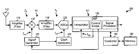
CA 02475974 2004-08-11
WO 03/069865 PCT/US03/04384
16
large a frequency error at any given time, especially when the outer timing
control loop
has just been turned on. This may be achieved by limiting (or saturating) the
absolute
value of the phase adjustment term, ecor , to a particular maximum value if
the magnitude
of the timing error, Zerr, is too large. This then avoids large frequency
error, especially
during the transient state, which may degrade demodulation performance.
Conversely, if
the timing error is too small and would have negligible impact on SINR, then
the phase
adjustment term, Bcor , may be set to zero. This then minimizes or reduces
steady-state
frequency jitter on the LO signal induced by the phase adjustment term.
[1061] In an embodiment, the phase adjustment term, Be r , may be expressed
as:
cor = K ''I'(zerr) . Eq (1)
[1062] In an embodiment, the transfer function, `F(rerr) , for the timing
error, Zerr, is
given by the following expression:
0 if I Zerr I C Zmin
V (Zerr) = G p Zerr if 'rr i. < I Zerr I C Zmax . Eq (2)
sign(Zerr) . GP I Zerr I if Zmax < I Zerr I
As shown in equation (2), when the magnitude of the timing error is neither
too large nor
too small, the function 'F(zerr) is linear in the timing error, Zerr= In a
specific
embodiment, the following values may be used for the parameters of equation
(2):
Z,,,;,, = 1/ 16 and GP I Zerr I= 20. Other design values may also be used and
are within the
scope of the invention.
[1063] The performance of the frequency-timing control loop may be analyzed,
and
performance metrics such as tracking bandwidths and steady-state jitter may be
determined in a manner known by one skilled in the art.
[1064] In many receiver implementations, the ADC sampling clock is tied to the
LO
frequency. Hence, changing ADC-sampler timing introduces transient frequency
errors in
the RF/IF downconversion mixers. Furthermore, a common local oscillator and a
common sampler are shared by all finger processors of the rake receiver.
Therefore, the
outer timing control loop affects the sampling instants for all finger
processors.
CA 02475974 2004-08-11
WO 03/069865 PCT/US03/04384
17
Consequently, the outer loop may be activated on one particular finger
processor (i.e., one
path/signal instance), while the inner loop may activated/de-activated
independently on
each signal instance. In other words, the inner timing control loop may be
operated
independently for each finger processor. Since the outer timing control loop
yields
performance gains mainly at high SINR, this loop may be operated so that the
ADC-
sampler timing is optimized for the signal instance with the highest SINR.
[1065] While the inner timing control loop is nearly independent of the
frequency
control loop, the outer timing control loop is tightly coupled with the
frequency control
loop as well as with the other inner loops operated by the individual finger
processors. It
is necessary to avoid undesired interactions (positive-feedback) between these
various
control loops, which could lead to instability.
[1066] In an embodiment, stability may be ensured by enabling the outer timing
control loop only when the SINR at one of the finger processors is reasonably
high (as to
justify performance gains). To also, ensure loop stability, the tracking
bandwidth, fTR,o,t ,
of the frequency-timing control loop with respect to the phase adjustment
term, 0,,,,, may
be designed to be smaller than both (1) the tracking bandwidth, fTR f , of the
frequency
control loop , and (2) the tracking bandwidth, fTR =õ , of the inner timing
control loop.
Stability may be ensured if the tracking bandwidth fTR,,,,, is a factor of two
or more
smaller than the tracking bandwidths fTR,f and fTR,;,,. In a specific design,
the tracking
bandwidth fTR,our may be designed to be several orders of magnitude smaller
than the
tracking bandwidths fTR f and fTR,,, .
[1067] For the forward link in an IS-856 system with a gated pilot
transmission
scheme, the frequency control loop may be designed to have a tracking
bandwidth on the
order of 100 Hz at high SINK, and a steady-state frequency jitter with a
standard deviation
of below 10 Hz.
[1068] The selection of a non-linear function, 1( ), for the transfer function
between
the timing error, Zerr, and the phase adjustment term, cor , as shown in
equation (2), is
driven by the need to reduce frequency jitter given the need to balance
conflicting design
requirements. The dead-zone in the function W( ) for small values of Zerr
(i.e.,
(Zerr) = 0, for IZerr 1:5 Zn in) ensures that yp = 0 when the receiver time
reference, tour,
CA 02475974 2004-08-11
WO 03/069865 PCT/US03/04384
18
is near-optimal. Saturation of the function W( ) for large values of Zerr
(i.e.,
W (rerr) = sign (2err) = GP I Zerr 1, for I Zerr I > Zmax) is intended to
limit the peak value of the
frequency error due to steady-state jitter of the timing loop filter output,
and the large
phase adjustment term 9cO, , when the receiver time reference, zout, is far
away from the
optimal time reference, Zu (i.e., during the transient period of the outer
timing loop
operation).
[1069] The frequency-timing control loop may be implemented based on various
designs. One specific design is described below.
[1070] FIG. 4 is a block diagram of a frequency-timing control loop 400 that
may be
used to acquire and track both the frequency and timing of a given signal
instance.
Frequency-timing control loop 400 includes a frequency control loop 230a and a
timing
loop filter 240a, which are one embodiment of frequency control loop 230 and
timing
loop filter 240, respectively, in FIG. 2.
[1071] Frequency control loop 230a includes a frequency discriminator 420
coupled
to a loop filter 430. Frequency discriminator 420 receives a pair of
consecutive complex
pilot symbols, PI (i) + JPQ (i) and PI (i -1) + JPQ (i -1) , from despread I &
D elements
222c, which are derived based on the on-time interpolated samples. Frequency
discriminator 420 then derives the frequency error metric, Ferr, for these
pilot symbols.
In particular, within frequency discriminator 420, a multiplier 422a receives
and
multiplies the imaginary part of the previous pilot symbol, PQ (i -1) , with
the real part of
the current pilot symbol, PI(i), and provides the product to a summer 424. A
multiplier
422b similarly receives and multiplies the real part of the previous pilot
symbol, P1(i -1) ,
with the imaginary part of the current pilot symbol, PQ (i) , and also
provides the product
to summer 424. Summer 424 then subtracts the product of multiplier 422a from
the
product of multiplier 422b and provides the frequency error metric, Ferr.
Other types of
frequency discriminator may also be used, and this is within the scope of the
invention.
[1072] In the embodiment shown in FIG. 4, loop filter 430 implements a first-
order
loop filter for the frequency control loop. Loop filter 430 includes a single
accumulator
comprised of a summer 436 and a register 438. The first loop filter input
(which is the
frequency error metric, Ferr, from frequency discriminator 420) is initially
scaled with a
scaling factor, KL, by a multiplier 432. The scaled value from multiplier 432
is then
CA 02475974 2004-08-11
WO 03/069865 PCT/US03/04384
19
combined with the second loop filter input (which is the phase correction
term, Pcor or
Boor , from timing loop filter 240a) by a summer 434, and the combined value
is
accumulated by the loop accumulator. The output from the accumulator comprises
the
frequency control loop output, Fctrll, which is provided to signal generator
122a. This
loop output is an estimate of the frequency error, Of, of the data samples.
[1073] Signal generator 122a is one embodiment of signal generator 122 in FIG.
1.
Within signal generator 122a, a signal converter 442 receives and conditions
the
frequency control loop output, Fctrll, to provide a control signal having a
suitable form
(e.g., a voltage or current). The control signal is then used to adjust the
frequency and
phase of a VCO 444. VCO 444 provides the LO signal to downconverter 116 and
(although not shown in FIG. 4) may further provide to clock generator 124 a
reference
signal used to derive the sampling clock for ADCs 120. The reference signal
may be a
divided down version of the LO signal. VCO 444 may be implemented with various
designs (e.g., as a single VCO, a VCO phase-locked to a VCXO, or based on some
other
design) as is known in the art.
[1074] In general, the frequency control loop output, Fctrll, is used to
adjust the
frequency and phase of a "periodic" signal that directly or indirectly
determines (1) the
frequency of the LO signal used to downconvert the received signal and (2) the
phase of
the clock signal used to digitize the downconverted signal. This periodic
signal may be
the LO signal itself, or an intermediate signal to which the LO and clock
signals may be
locked to via one or more phase lock loops (PLLs), as is known in the art. The
reference
signal provided by the signal generator to the clock generator may be the ADC-
sampling
clock itself. Alternatively, the ADC-sampling clock may be derived based on
the
reference signal (e.g., by dividing down the reference signal or by locking
another VCO to
the reference signal).
[1075] In the embodiment shown in FIG. 4, timing loop filter 240a implements a
second-order loop filter for the timing control loop. Timing loop filter 240a
includes a
first accumulator comprised of a summer 474a and a register 476a, and a second
accumulator comprised of a summer 474b and a register 476b. The timing loop
filter
input (which is the timing error metric, Terr, from the timing discriminator
shown in FIG.
2) is initially scaled with a scaling factor, co, by a multiplier 472a and
also scaled with a
scaling factor, cl, by a multiplier 472b. The scaled value from multiplier
472b is then
CA 02475974 2004-08-11
WO 03/069865 PCT/US03/04384
accumulated by the first accumulator. The output from the first accumulator is
combined
with the scaled value from multiplier 472a by summer 474b, and the combined
value is
further accumulated by the second accumulator.
[1076] For the inner timing control loop, a quantizer 478 quantizes the output
from
the second accumulator (which corresponds to the timing difference, 2d1ff, in
the outer
timing control loop model in FIG. 3) to a particular desired resolution (e.g.,
Tc/8), as
required by the interpolator used to re-sample the data samples from the ADCs.
Upon
achieving both frequency and timing lock for a given signal instance with the
outer timing
control loop, the signal instance is sampled at the optimal (or near optimal)
sampling time
instants, and interpolation is not required for this signal instance. However,
if the outer
timing control loop is not enabled, or for a signal instance for which the
outer timing
control loop is not available, then quantizer 478 (within the inner timing
control loop)
provides the re-sampler timing control, Tctrl, used for interpolation. The
output from
quantizer 478 corresponds to the time offset, radj, in the frequency-timing
control loop
model in FIG. 3).
[1077] For the outer timing control loop, the output from the second
accumulator is
provided to a Mod element 482, which performs modulo-M operation, where M =
TS/T,,,
TS is the sample period, and Tc is the chip period. If the sample rate is
chipx2, then Ts=
TJ2 and M = 1/2. If M is a power of twos, then the modulo-M operation may be
performed by omitting some of the more significant bits (MSBs) from the second
accumulator and passing the remaining less significant bits (LSBs). The output
from Mod
element 482 corresponds to the timing error, Ter,., in the frequency-timing
control loop
model in FIG. 3).
[1078] A transfer gain element 490 receives the timing error from Mod element
482
and provides the phase correction term, Pcor, based on a particular transfer
function, e.g.,
the one shown in equation (1). In an embodiment, this transfer function
includes a non-
linear function such as the one shown in equation (2). Transfer gain element
490 also
receives an Enable signal, which indicates whether or not the outer timing
control loop is
enabled. Transfer gain element 490 provides valid phase correction term, Pcor,
if the
outer timing control loop is enabled (e.g., the Enable signal is at logic
high) or zero
otherwise.
CA 02475974 2011-07-29
74769-936
21
[1079] FIG. 4 shows a specific design for each of the components of the
frequency-
timing control loop. Other designs that may be used for the frequency
discriminator and
loop filters are described in numerous references available in the art. One
such reference
is a book by A.J. Viterbi, entitled "Principles of Spread Spectrum Multiple
Access
Communications," 2nd Ed., McGraw Hill, 1977.
[1080] As noted above, DSP 130 may implement a rake receiver that includes a
number of finger processors, each of which may include a frequency control
loop and a
timing control loop to respectively acquire and track the frequency and timing
for the
signal instance assigned to the finger processor. Since downconversion and A-
to-D
conversion (ADC) is common to all multipath-instances in the received signal,
the
frequency of the LO signal used for the downconversion and the phase of the
clock
signals used for the ADC-sampling may be adjusted for only one signal instance
in the
received signal. This signal instance may be selected as the strongest signal
instance that
exceeds a particular threshold (e.g., 4.5 dB).
[1081] The outer timing control loop may thus be enabled for one signal
instance. For
this signal instance, rotation and interpolation of the data samples are not
needed since its
frequency and timing are adjusted based on the LO signal and the ADC-sampling
clock,
respectively. For each of the other signal instances that may be concurrently
processed
along with this signal instance, rotator 212 may be used to correct for the
signal instance's
residual frequency error and interpolator 214 may be used to correct for the
signal
instance's residual timing error.
[1082] The techniques described herein may be implemented by various means.
For
example, the frequency-timing control loop may be implemented in hardware,
software,
or a combination thereof. For a hardware implementation, the elements of the
frequency-
timing control loop may be implemented within one or more application specific
integrated circuits (ASICs), digital signal processors (DSPs), digital signal
processing
devices (DSPDs), programmable logic devices (PLDs), field programmable gate
arrays
(FPGAs), processors, controllers, micro-controllers, microprocessors, other
electronic
units designed to perform the functions described herein, or a combination
thereof.
[1083] For a software implementation, all or portions of the frequency-timing
control
loop may be implemented with modules (e.g., procedures, functions, and so on)
that
perform the functions described herein. The software codes may be stored in a
memory
CA 02475974 2004-08-11
WO 03/069865 PCT/US03/04384
22
unit (e.g., memory 142 in FIG. 1) and executed by a processor (e.g., DSP 130
or
controller 140). The memory unit may be implemented within the processor or
external
to the processor, in which case it can be communicatively coupled to the
processor via
various means as is known in the art.
[1084] The frequency-timing control loop may also be implemented with a
combination of hardware and software. For example, hardware may be used to
derive the
pilot symbols, and software may be used to implement the frequency
discriminator,
frequency loop filter, and timing loop filter.
[1085] Headings are included herein for reference and to aid in locating
certain
sections. These headings are not intended to limit the scope of the concepts
described
therein under, and these concepts may have applicability in other sections
throughout the
entire specification.
[1086] The previous description of the disclosed embodiments is provided to
enable
any person skilled in the art to make or use the present invention. Various
modifications
to these embodiments will be readily apparent to those skilled in the art, and
the generic
principles defined herein may be applied to other embodiments without
departing from
the spirit or scope of the invention. Thus, the present invention is not
intended to be
limited to the embodiments shown herein but is to be accorded the widest scope
consistent
with the principles and novel features disclosed herein.
[1087] WHAT IS CLAIMED IS: