Note: Descriptions are shown in the official language in which they were submitted.
CA 02477299 2004-08-23
WO 03/087707 PCT/US03/11053
METALLIZATION OF CARBON NANOTUBES
FOR FIELD EMISSION APPLICATIONS
TECHNICAL FIELD
The present invention relates in general to nanostructured materials, and in
particular, to using
modified carbon nanotubes for field emission applications.
BACKGROUND INFORMATION
Carbon nanotubes (CNTs) are currently being investigated for use as cold
electron sources in a
variety of applications. These include displays, microwave sources, x-ray
tubes, etc. For CNTs to be used as
a cold cathode, they must be placed on a conductive surface (conductive
substrate or conductive film on a non-
conductive substrate). This has led some to place catalysts on the substrate
surface and grow the carbon
nanotubes in situ using CVD techniques (Kim et al., J. Appl. Phys., 90(5),
2591 (2001)). However, this has
several draw-backs. This technique typically grows multi-wall carbon nanotubes
(MWNTs). However,
MWNTs have poorer field emission quality compared to single-wall carbon
nanotubes (SWNTs) (Karachi et al.,
"FED with double-walled carbon nanotube emitters," the 215' International
Display Research Conference in
Conjunction with the 8"' International Display Workshops, Nagoya Congress
Center, Nagoya, Japan, Oct. 16-19,
2001, pp. 1237-1240). The substrate is subjected to high temperature,
typically above 600°C, limiting the
substrates that can be used. Uniformity is difficult to achieve because of the
high temperature growth processes
required. As a result, the manufacture of cathodes using this process will be
very expensive due to the number
and complexity of post-processing steps needed to generate a material capable
of producing the desired level of
field emission.
Other investigations have centered on processes for making CNT cathodes in a
separate process,
collecting them, and then dispensing them onto a substrate using a variety of
techniques (I~im et al., I?iarnond
and Related Materials, 9, 1184 (2000)). This has several advantages over the
in situ method described above.
First, the fabrication of the CNT material is decoupled from the fabrication
of the cathode. This permits
choosing the optimal CNT material for the application (single-wall, double-
wall, mufti-wall, purified, non-
purified, etc.). Second, the dispensing process is carried out a relatively
low-temperatures, permitting greater
flexibility in the choice of substrates. Third, uniform deposition over large
area substrates is far more feasible
using currently-available, low-cost equipment. Current dispensing processes,
however, have their disadvantages.
One of these is that the CNT fibers are often dispensed such that they clump
together or are imbedded inside
another material (Kim et al., "Toward a ridge of carbon nanotube FEDs," the
215' International Display Research
Conference in Conjunction with the 8~' International Display Workshops, Nagoya
Congress Center, Nagoya,
Japan, Oct. 16-19, 2001, pp. 1221-1224). These factors limit the performance
of the CNT material. "Activation"
processes are often employed after dispensing _the CNT material. These
processes recover some of the
performance of the virgin CNT (Chang et al., U.S. Patent No. 6,436,221 B1).
These "activation" process steps,
-1-
CA 02477299 2004-08-23
WO 03/087707 PCT/US03/11053
however, can add cost to the product and may lead to non-uniform performance.
Yet another disadvantage of
current dispensing techniques is that the dispensed CNT fibers may not have
sufficiently good contact to the
substrate or the substrate's conductive layer such that this impedes their
ability to supply the electrons needed for
field emission.
It has been recently found that by mixing CNT material with other nanoparticle
materials, the field
emission properties of the CNT were improved (Mao et al., U.S. Provisional
Application No. 60/417,246,
incorporated herein by reference). Because neighboring nanotubes shield the
extracted electric fields from each
other (Bonard et al., Adv. Mat., 13, 184 (2001)), it is believed that this
improvement is a result of induced
separation of the CNT material by the nanoparticles. In situations where the
CNT fibers are too close, they may
electrically screen the applied electric field from each other. By increasing
the separation between the fibers, the
effective applied field strength at the emission sites is higher.
Many SWNT fibers are semiconducting with a bandgap that is dependent upon the
chiral indices (n,m)
of the SWNT. Choi et al. (US Patent 6,504,292 B1) teach that, for field
emission applications, this bandgap can
be overcome by depositing a metal film on CNT fibers that are already attached
to a substrate. Choi et al. teach
that the CNT fibers are coated after the fibers are grown using CVD
techniques. This method has the inherent
aforementioned disadvantages of growing CNTs on the substrate. Furthermore,
were the CNT fibers to be
dispensed onto the substrate and then coated, the problems of separating the
CNT fibers for improved emission
would still remain.
A method of aligning CNTs is disclosed in U.S. Patent No. 6,312,303 B1 to
Yaniv et al. (incorporated
herein by reference), whereby CNTs are aligned by including the CNTs in a host
material, aligning the host
material (such as liquid crystal material) and the host phase material then
aligns the CNTs.
BRIEF DESCRIPTION OF THE DRAWINGS
For a more complete understanding of the present invention, and the advantages
thereof, reference is
now made to the following descriptions taken in conjunction with the
accompanying drawings, in which:
FIGURE 1 illustrates metallized carbon nanotubes on indium-tin-oxide
(ITO)/glass, wherein the metal
coating is not necessarily uniform over all of the carbon nanotubes (CNTs);
FIGURE 2 illustrates an embodiment wherein metallized carbon nanotubes are
magnetically-aligned
while being dispensed;
FIGURE 3 illustrates a field emission display device incorporating the present
invention;
FIGURE 4 illustrates an electroless plating bath used to coat carbon nanotubes
with metal;
FIGURE 5 illustrates field emission current vs. electric field for cobalt-
coated and non-coated carbon
nanotubes;
_2-
CA 02477299 2004-08-23
WO 03/087707 PCT/US03/11053
FIGURE 6 illustrates an embodiment wherein a cathode substrate was placed on a
set of six
permanent magnets prior to dispensing magnetically-aligned metallized CNTs
onto the substrate;
FIGURE 7 illustrates the arrangement of the six permanent magnets in FIGURE 6
prior to placing the
ITO/glass substrate and dispensing the magnetically-aligned CNTs onto the
substrate wherein the face of each
of the block magnets is magnetized North-South as shown in the edge (side)
view; and
FIGURE ~ illustrates field emission in a display device wherein the cathode
comprises magnetically-
active metallized CNTs which were dispensed onto a substrate with magnets
behind it, as in FIGURE 7.
DETAILED DESCRIPTION
The present invention is directed towards metallized carbon nanotubes, methods
for making
metallized carbon nanotubes; methods for dispensing metallized carbon
nanotubes onto a substrate; methods
for aligning metallized carbon nanotubes; cold cathode field emitting
materials comprising metallized carbon
nanotubes, aligned metallized carbon nanotubes, and combinations thereof; and
methods of using metallized
carbon nanotubes as cold cathode field emitters.
Metallized carbon nanotubes, according to the present invention, are carbon
nanotubes which have
been at least partially coated with one or more metals. Carbon nanotubes,
according to the present invention,
include, but are not limited to, single-wall carbon nanotubes, multi-wall
carbon nanotubes, double-wall carbon
nanotubes, buckytubes, carbon fibrils, derivatized carbon nanotubes,
chemically-modified carbon nanotubes,
metallic carbon nanotubes, semiconducting carbon nanotubes, and combinations
thereof. Purity of the carbon
nanotube reactant materials (i.e., the carbon nanotubes prior to being
metallized) ranges generally from at least
about 1 percent to at most about 100 percent, specifically from at least about
10 percent to at most about 100
percent, and more specifically from at least about 20 percent to at most about
100 percent. Carbon nanotubes,
as described herein, can exist in bundles or as individual entities.
Furthermore, the carbon nanotubes from
which the metallized carbon nanotubes are derived can be produced by any
process which suitably provides
for carbon nanotubes according to the present invention.
Metal coatings (also termed "films") on the carbon nanotubes comprise one or
more metal layers and
range generally in thickness from at least about 0.1 nanometer (nm) to at most
about 10 micrometers (pm),
specifically from at least about 0.1 nanometer to at most about 1 micrometer,
and more specifically from at
least about 0.5 nanometers to at most about 1 micrometer. Metal coatings on
the carbon nanotubes include,
but are not limited to nickel (Ni), iron (Fe), copper (Cu), silver (Ag), zinc
(Zn), rhodium (Rh), tin (Sn),
cadmium (Cd), chromium (Cr), beryllium (Be), palladium (Pd), indium (In),
platinum (Pt), gold (Au), and
combinations thereof. In some embodiments, the metal coating comprises an
alloy of two or more metals. In
some embodiments, the metal coating comprises multiple layers of differing
metals or alloys. In some
embodiments, the metal coating comprises metals which are magnetically-active
in that they exhibit an affinity
for aligning along magnetic field lines when placed in a magnetic field. The
weight percent of metal in the
-3-
CA 02477299 2004-08-23
WO 03/087707 PCT/US03/11053
metallized carbon nanotube product ranges generally from at least about 0.1
percent to at most about 99
percent, specifically from at least about 1 percent to at most about 99
percent, and more specifically from at
least about 5 percent to at most about 99 percent. In some embodiments of the
present invention, these metal
coatings are highly uniform over individual carbon nanotubes. In some
embodiments, these metal coatings are
non-uniform, non-continuous, and/or incomplete, as depicted in FIGURE 1
wherein metal coating 105 is
shown on carbon nanotubes 104 to form metallized carbon nanotubes 106. In some
embodiments these metal
coatings are deposited primarily on the exterior of carbon nanotube bundles.
In some embodiments, bundles
of carbon nanotubes are metallized within the interior of the bundle. In some
embodiments, the carbon
nanotubes are metallized endohedrally, inside the tube structure. Some
embodiments comprise metallized
carbon nanotubes with any combinations) of the aforementioned metallized
carbon nanotubes.
Exemplary methods of making metallized carbon nanotubes comprise the steps of:
a) providing a
plurality of carbon nanotubes; b) preparing an electroless metal plating
solution; c) adding said carbon
nanotubes to said electroless metal plating solution to form a reaction
solution; d) subjecting said reaction
solution to a reducing condition which causes metal ions in solution to be
reduced to metal and nucleate on the
carbon nanotubes to produce metallized carbon nanotubes; and e) removing said
metallized carbon nanotubes
from the reaction solution. In some embodiments of the present invention, the
metallized carbon nanotubes
are washed and dried after being removed from the reaction solution.
Carbon nanotubes, as described herein, can be carbon nanotubes of any
dimension, chirality, and
number of walls that suitably provides for carbon nanotubes of the present
invention and include, but are not
limited to, single-wall carbon nanotubes (SWNTs), mufti-wall carbon nanotubes
(MWNTs), double-wall carbon
nanotubes (DWCTs), buckytubes, carbon fibrils, derivatized carbon nanotubes,
chemically-modified carbon
nanotubes, metallic carbon nanotubes, semiconducting carbon nanotubes, and
combinations thereof. In some
embodiments of the present invention, the carbon nanotubes are treated with
hydrochloric acid prior to the
metallization step.
An electroless plating solution (commonly referred to as a plating bath),
according to the present
invention, comprises a solvent, a metal salt, and a reducing agent (See Ranney
et al., Electroless Plating and
Coating of Metals," Noyes, Park Ridge, NJ (1972), incorporated herein by
reference, for a detailed description
of electroless plating techniques). In some embodiments of the present
invention, there is a promoter species
which helps to dissolve the metal salt. In some embodiments, there may be a
balancing agent to control the
pH. The solvent can be any solvent which suitably provides for the solvation
of the electroless plating
solution components. An exemplary solvent is water. The metal salt can be any
metal salt that suitably
provides for electroless metal plating according to the present invention and
includes, but is not limited to,
salts of the following: nickel, iron, copper, silver, zinc, rhodium, tin,
cadmium, chromium, beryllium,
palladium, indium, platinum, gold, and combinations thereof. In some
embodiments, alloys of two or more
metals are plated on the carbon nanotubes with this process. The reducing
agent can be any reducing agent
that suitably provides for the reduction of the metal salt according to the
present invention and includes, but is
not limited to NaHzPO2~Hz0, NZH4~2HC1, NzH4~xH20, and combinations thereof.
The optional promoter
-4-
CA 02477299 2004-08-23
WO 03/087707 PCT/US03/11053
species can be any species which suitably promotes the electroless metal
plating process of the present
invention by facilitating the dissolution of the metal salt in the solution.
Suitable promoter species include, but
are not limited to C4H4O6KNa~4HZO, NaZC4H4O6, Na3C6H50~~2Hz0, and combinations
thereof. The optional
balancing agent can be any species which suitably provides for the control of
pH according to the present
invention. Suitable balancing agents include, but are not limited to NaOH,
I~OH, NH40H, and combinations
thereof.
In some embodiments of the present invention, the process of adding the carbon
nanotubes to the
electroless plating solution is carried out by first ultrasonicating the
carbon nanotubes in a suitable solvent just
prior to addition. This enhances their dispersal in the electroless plating
solution to form a reaction solution.
This reaction solution is subjected to a reducing condition which causes metal
ions in solution to be reduced to
metal and nucleate on the carbon nanotubes to produce metallized carbon
nanotubes. Reducing conditions,
according to the present invention, are any conditions which suitably provide
for a reduction of the metal ions
in solution. Such reducing conditions induce this reduction and include, but
are not limited to, heating,
irradiation, chemical activation, and combinations thereof. In some
embodiments, the electroless plating
solution is subjected to the reducing condition prior to the addition of the
carbon nanotubes.
In some embodiments of the present invention, the degree of carbon nanotube
metallation (i.e., the
amount of metal coated on the carbon nanotubes) is modulated by the amount of
carbon nanotubes present in
the reaction solution. In other embodiments, the degree of carbon nanotube
metallation is modulated by the
concentration of metal salts and reducing agents present in the reaction
solution. In other embodiments, the
degree of carbon nanotube metallation is modulated by the time the carbon
nanotubes spend in the reaction
solution. In still other embodiments, a combination of one or more of the
aforementioned methods of
modulating the degree of carbon nanotube metallation is used to produce a
metallized carbon nanotube
product with certain desired characteristics dependent upon the degree in
which is has been metallized.
In some embodiments of the present invention, prior to the step of removing
the metallized carbon
nanotubes from the reaction solution, a stabilizing agent is added to slow the
reduction of the metal ions. A
stabilizing agent can be any species which suitably provides for the slowing
of the reduction process of the
present invention and includes, but is not limited to, H3B03, C3H603, and
combinations thereof. Such slowing of
the reaction facilitates greater control over the nature of the end product.
Suitable methods of removing the
metallized carbon nanotubes from the reaction solution include, but are not
limited to, centrifugation (and
subsequent decantation), filtration, and combinations thereof. In some
embodiments of the present invention,
after the step of removing the metallized carbon nanotubes from the reaction
solution, there is a step of washing
the metallized carbon nanotube product. Suitable washing solvents include any
solvent which suitably removes
unwanted reactants or reaction products from the final product. Suitable
solvents include, but are not limited to,
water, isopropyl alcohol, acetone, and combinations thereof. Optional drying
of the metallized carbon nanotube
product can be carned out by any drying process which suitably provides for
the drying of the metallized carbon
nanotubes according to the present invention and includes, but is not limited
to, heating, exposure to vacuum,
vacuum heating, irradiation, and combinations thereof.
-5-
CA 02477299 2004-08-23
WO 03/087707 PCT/US03/11053
Exemplary methods of dispensing metallized carbon nanotubes onto a substrate
comprise: a)
dispersing the metallized carbon nanotubes in a solvent to form a suspension;
and b) applying the suspension
to a substrate using an "applicator means." Solvents into which the metallized
carbon nanotubes are dispersed
include, but are not limited to, isopropanol, methanol, acetone, water,
ethanol, and combinations thereof.
Methods of dispersing the metallized carbon nanotubes in the solvent include,
but are not limited to, stirring,
shaking, ultrasonic assistance, and combinations thereof. FIGURE 1 illustrates
one embodiment of metallized
carbon nanotubes 106 on a substrate 103:
An applicator means, according to the present invention, can be any method
which suitably dispenses
the suspension of metallized carbon nanotubes onto a substrate in a controlled
manner. Such application can
be uniform or non-uniform, and can vary considerably in terms of the thickness
of the resulting film, or layer,
of metallized carbon nanotubes on the substrate. Suitable applicator means
include, but are not limited to,
printing, dispensing, painting, spaying, brushing, and combinations thereof.
Suitable printing methods
include, but are not limited to, inkjet printing, screen printing, off set
printing, and combinations thereof. An
exemplary applicator means comprises a spraying technique whereby the
suspension of metallized carbon
nanotubes is sprayed onto a surface using a sprayer. While not intending to be
bound by theory, a sprayer,
according to the present invention, can be a pump sprayer which rapidly pushes
the suspension through a
small orifice and, upon exiting said orifice, the suspension becomes an
aerosol of small suspension droplets
which are directed toward the substrate surface. Optionally, the substrate can
be heated during the application
process to prevent the running of excess solvent. Typically, the substrate,
after having applied the metallized
carbon nanotubes to its surface, is dried to remove any excess solvent. A
substrate, as described herein, can be
any substrate which suitably provides for a surface on which to dispense
metallized carbon nanotubes
according to the present invention and includes, but is not limited to,
metals, ceramics, glass, semiconductors,
coated surfaces, layered materials, and combinations thereof.
In some embodiments of the present invention, the metallized carbon nanotubes
are dispensed onto a
substrate while under the influence of a magnetic field. In embodiments such
as these, and when the
metallized carbon nanotubes have a magnetically-active coating, the metallized
carbon nanotubes can be
aligned or oriented in a desired manner. In some embodiments of the present
invention, the metallized carbon
nanotubes are magnetically-aligned subsequent to their being dispensed on a
substrate. Magnetic alignment,
according to the present invention, can be achieved with one or more magnets
selected from the group
consisting of permanent magnets, electromagnets, and combinations thereof.
Various embodiments of the
present invention comprise magnetic fields which include, but are not limited
to, magnetic fields which are
uniform, non-uniform, directed, mufti-directional, isotropic, anisotropic,
continuous, pulsed, and combinations
thereof. In some embodiments, a magnetic field is applied to an entire
substrate while a dispensing head is
rastered over the substrate surface. In some embodiments, the magnetic field
is highly localized and is itself
rastered along with a dispensing head over the substrate surface. In some
embodiments of the present
invention, the substrate is magnetic. Magnetic alignment, according to the
present invention, is a very clean
process in that, unlike existing alignment processes (Chang et al., U.S.
Patent No. 6,436,221), nothing is
required to come into contact with the nanotube surface in order to generate
such alignment. Furthermore, in
-6-
CA 02477299 2004-08-23
WO 03/087707 PCT/US03/11053
some embodiments of the present invention, the magnetic alignment process can
be "patterned" such that
some regions of the nanotube layer dispensed on a substrate are aligned in one
direction, and are aligned in
other directions in other regions. These directions can be with magnetic
"north" either vertical to the plane (up
or down) or in the plane, or any combination of in-plane and out-of plane
(slanted). The alignment process
can be carried out either during the carbon nanotube deposition or after
deposition.
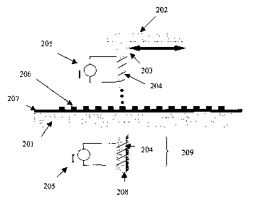
FIGURE 2 illustrates an embodiment wherein metallized carbon nanotubes are
magnetically-aligned
while being dispensed. Referring to FIGURE 2, a dispensing head 202, which
dispenses magnetic, metallized
CNTs and which moves in X and/or Y directions, is rastered over substrate 201.
As the magnetic, metallized
CNTs are forced through nozzle 203, they are aligned with a magnetic field
generated by coils 204 and power
supply 205. Dispensed drops 206 of magnetically-aligned metallized CNTs can
thus be deposited in any
arrangement or orientation on a substrate surface. Optionally, an additional
magnet 209 comprising a
magnetic core 208 can be used to fizrther direct the dispensing process and
orient the magnetic, metallized
CNTs. In some embodiments, an optional coating 207 is applied to the substrate
before commencing with
dispensing of the magnetic, metallized CNTs.
In some embodiments, as described later, permanent magnets can be arranged on
one or both sides of
substrate 201 to assist in aligning magnetically-active metallized CNTs during
dispensing. Magnetic fields
can also be supplied by larger electromagnetic coils that do not move with the
dispensing head.
In some embodiments of the present invention, an electro-magnetic head is
rastered over a surface,
after magnetically-active metallized CNTs have been dispensed onto said
substrate. Such rastering produces
patterned alignment. In these embodiments, the electro-magnetic head writes a
pattern into a surface much
like a read/write head writes a pattern to a magnetic surface of a disk in a
data storage "hard drive" of a
computer.
In some embodiments of the present invention, metallic carbon nanotubes are
dispensed with
nanoparticles in a manner described previously for the dispensing of
unmetallized carbon nanotubes with
nanoparticles (United States Provisional Patent Application, Serial No.
601417,246, incorporated herein by
reference). Such nanoparticles have compositions which include, but are not
limited to, metals, semimetals,
fullerenes, semiconductors, dielectrics, ceranucs, metalloids, glasses,
polymers, and combinations thereof. In
some embodiments, the nanoparticles are magnetically active. In some
embodiments, magnetically-active
metallized carbon nanotubes are dispensed with magnetically-active
nanoparticles. In such embodiments,
local magnetic field strength can be increased during the alignment process,
thus leading to potentially higher
degrees of alignment of the metallized carbon nanotubes.
In some embodiments of the present invention, the metallized carbon nanotubes
are used for field-
emission application. In some embodiments, these metallized carbon nanotubes
are more suitable for field
emission applications than carbon nanotubes without a metal coating. While not
intending to be bound by
theory, it is likely that, when incorporated into a device for field emission
applications, the metallized carbon
nanotubes are better separated from one another, creating a carbon nanotube
arrangement of lower density that
_7_
CA 02477299 2004-08-23
WO 03/087707 PCT/US03/11053
reduces the shielding effects contributed by neighboring carbon nanotubes.
Furthermore, said metal coatings
likely enhance the flow of electrons in semiconducting carbon nanotubes and at
the nanotube-substrate junction.
In some embodiments of the present invention involving field emission
applications, the metallized carbon
nanotubes are dispensed onto a substrate using an applicator means, and the
resulting substrate (with the
metallized carbon nanotubes) is used as the cathode in, for example, a field
emission display. Other field
emission applications in which metallized carbon nanotubes can be used
include, but are not limited to X-ray
sources, electron sources, rf arrays, microwave tubes, and combinations
thereof.
In some embodiments of the present invention wherein metallized CNTs are
dispensed onto a substrate
surface for use as a cathode in field emission application, an optional taping
process can be used to "activate" the
CNT layer and produce better field emission. In such embodiments, an adhesive
film or tape is placed on top of
the CNT layer such that the adhesive is put in contact with the CNTs. The tape
is then removed at an appropriate
angle such that the CNTs on the surface of the layer can be vertically aligned
to further enhance field emission
properties. Such activation has been described previously for field emission
cathodes comprising non-metallized
CNTs (Chang et al., U.S. Patent No. 6,436,221 B1; Yaniv et al., U.S.
Provisional Patent application Serial No.
60/348,856; both of which are incorporated herein by reference). Embodiments
using magnetic alignment may
obviate this step.
Thus, as disclosed herein, the present invention is also directed towards an
improved field emission
cathode using carbon nanotube emitters that are first coated with a metal film
and then dispensed onto the
cathode. This field emission cathode is illustrated in FIGURE 1. Referring to
FIGURE 1, metallized carbon
nanotubes 106 are shown on a substrate 103 which comprises a conductive layer
102 and an optional layer 101,
which can be either conductive or non-conductive. Collectively, this forms
field emission cathode 100. This
cathode has advantages over the current art in that: a) the metal layer
provides a high level of electrical
conductivity along the length of the CNT fiber even if the fiber is
semiconducting; b) t~e metal layer provides an
additional means of separating the CNT fibers from each other, decreasing the
mutual electrical shielding and
eliminating the need for post-deposition activation steps; c) metal-coated
carbon fibers adhere to metal layers on
the substrate much more strongly than do bare carbon nanotubes (adhesion
forces between metals are much
stronger than the adhesion forces between the substrate and the un-metallized
carbon nanotubes); and the metal
coatings can be applied to SWNTs and MWNTs, semiconducting or metallic CNTs,
purified or non-purified
CNTs-all using standard electrolytic techniques permitting selection from a
large variety of available CNT
fibers. Furthermore, in some embodiments of the present invention, the
improved field emission cathode
comprises metallized CNTs which can be magnetically-aligned. Magnetic
alignment of these metallized carbon
nanotubes within the field emission cathode can be in any desired orientation,
and can include any or all of the
metallized carbon nanotubes. Alignment can be patterned or uniform. Improved
field emission from non-
metallized carbon nanotube-based field emission cathodes has been realized
when the nanotubes are vertically
aligned (See United States Provisional Patent Application, Serial No.
60/348,856, incorporated herein by
reference).
_g_
CA 02477299 2004-08-23
WO 03/087707 PCT/US03/11053
Referring to FIGURE 3, the field emission cathode described above can be
incorporated into field
emission display 300. On substrate 301, conductive layer 302 is deposited and
metallized carbon nanotube layer
303 is deposited on top thereof. The anode includes substrate 304, which may
be a glass substrate, conductive
layer 305, which may be indium-tin-oxide, and a phosphor layer 306 for
receiving electrons emitted from
metallized carbon nanotube layer 303. Electrons are emitted from layer 303 in
response to an appropriate electric
field between the anode and the cathode.
In some embodiments of the present invention, carbon nanotubes are coated with
a magnetically-
active, but non-metallic species. Coated nanotubes such as these can be made
by first depositing a metal
coating, as described above, and then reacting this coating with other
chemicals, such as an oxidant (e.g.,
oxygen), to form compounds that are no longer metallic, but which are still
magnetic. In other embodiments,
such non-metallic magnetically-active coatings are chemically precipitated out
of a solution onto the carbon
nanotubes. An example of a non-metallic magnetically-active material which can
be applied to carbon
nanotubes as a coating is magnetite (Fe304). Methods of depositing magnetite
in this manner are known in the
art (Berger et al., "Preparation and Properties of an Aqueous Ferrofluid," J.
Chem. Edu., 76(7), 943 (1999);
Palacin et al., "Patterning with Magnetic Materials at the Micron Scale,"
Chenz. Mater'., 8, 1316 (1996); both
of which are incorporated herein by reference). One suitable method of
depositing magnetite on carbon
nanotubes involves preparing an aqueous solution comprising a mixture of
Fe(II) and Fe(III) halides and then
reacting this with ammonium hydroxide in the presence of carbon nanotubes. The
iron then precipitates out of
solution as Fe304, coating the carbon nanotubes in the process. A surfactant
may be employed to facilitate
dispersion of the carbon nanotubes within this solution.
In other embodiments of the present invention, other types of nanostructured
materials can be used in
place of carbon nanotubes. These other nanostructured materials can be
metallized, dispensed on a substrate,
and, if metallized with a magnetically-active metal, they can be aligned-all
in the same manner in which the
metallized carbon nanotubes are. Such nanostructures materials include, but
are not limited to, boron nitride
nanotubes, and nanowires of silicon, silicon carbide, gallium nitride, indium
phosphide, and combinations
thereof.
The process, according to the present invention, of first coating CNTs with
metal and then dispensing
them onto a substrate has a number of advantages, particularly for filed
emission applications. Such a method of
dispensing CNTs onto a substrate serves to inhibit clumping, provides for
sufficiently good contact to the
substrate, overcomes the limitations imposed by semiconducting CNTs, and it
obviates the need for activation
processes. Yet another advantage, in embodiments where the metal coating is
magnetically active, is the ability
to align the metal coated CNTs before, during, or after deposition.
The following examples are provided to more fully illustrate some of the
embodiments of the present
invention. The examples illustrate methods by which metal-coated (metallized)
CNTs can be made and prepared
for field emission applications. It should be appreciated by those of skill in
the art that the techniques disclosed
in the examples which follow represent techniques discovered by the inventor
to function well in the practice of
-9-
CA 02477299 2004-08-23
WO 03/087707 PCT/US03/11053
the invention, and thus can be considered to constitute exemplary modes for
its practice. However, those of skill
in the art should, in light of the present disclosure, appreciate that many
changes can be made in the specific
embodiments which are disclosed and still obtain a like or similar result
without departing from the spirit and
scope of the invention.
EXAMPLES
EXAMPLE 1. Coating single-wall carbon nanotubes with a Cobalt thin film
This process provides a way of depositing a metal thin film or coating on the
surface of carbon
nanotubes using an electroless plating technique. Using this relatively
inexpensive and simple process,
metallized carbon nanotubes can be made efficiently in relatively large
amounts.
The single-wall carbon nanotube (SWNT) material used here was purchased from
Iljin Nanotech, Inc.
(Korea). The length of the SWNTs ranged from approximately several micrometers
to approximately 20
micrometers, and the diameters were generally less than about 2 nanometers.
Referring to FIGURE 4, electroless plating apparatus 400 comprises an
electroless plating solution 404
contained in a beaker 403 which in turn is immersed in a water bath 402. Water
bath 402 is heated by a magnetic
stirring hotplate 401 and temperature is monitored by thermometer 406.
Stirring is accomplished with stir bars
405 activated by the magnetic stirring hotplate 401 and the stirring motor
407. In the present example,
electroless plating solution 404 comprises water and the following chemicals:
1. A cobalt (Co) salt (CoS04~7H20) to provide Co ions (Note that other salts
may be used, e.g.,
CoClz~6H20). Concentration of this component is approximately 20-28 grams per
liter.
2. A reducing agent (NaHzPO2~H20) to reduce Co ions to Co(0). Concentration of
this component is
approximately 18-25 grams per liter.
3. A promoter species to facilitate dissolution of the Co salt into the
solution (C4H406KNa~4Hz0).
Concentration of this component is approximately 140-160 grams per liter.
4. A stabilizing agent (H3B03), to slow the reducing reaction. Concentration
of this component is 27-35
grams per liter.
5. A balancing agent (NaOH). This is used to control the pH value of the
solution. The amount of this
material that is used is that needed to maintain a pH of 8-10 for the metal
plating solution.
The above chemicals were dissolved in deionized water up to 900 milliliters.
The cobalt ions in this solution undergo reduction under a reducing condition
of approximately 85-
95°C. The pH of the solution needs to be controlled before and during
the reaction. In this example, the pH
value was maintained at about 9. NaOH was added during the plating process to
control the pH of the solution.
Approximately 3-4 grams of carbon nanotube powder is ultrasonicated in a
beaker containing
approximately 100 milliliters of water for several minutes before being
introduced into the electroless plating
-10-
CA 02477299 2004-08-23
WO 03/087707 PCT/US03/11053
solution (after addition, total solution is 1000 milliliters). After the
solution is prepared, it is heated in a water
bath to 85-95°C and the ultrasonicated SWNTs are then added to the
electroless plating solution quickly while
the solution was stirred. Because the carbon nanotubes easily clump together,
the water+CNT mixture should
be ultrasonicated immediately before adding it to the plating solution. The
typical reaction time in the plating
solution is about 5-10 minutes. Longer times do not appear to affect the
results greatly. During the reaction, gas
is evolved from the solution. The solution is pink at the beginning but
gradually turns colorless. At the end of
the reaction, little or no gas is evolved from the solution.
After reaction/deposition of metal, the reaction beaker is taken out of the
water bath and allowed to cool
down to room temperature. After several minutes, the metallized carbon
nanotube powders collect at the bottom
of the beaker and the solution is decanted from the powder. The powder is
washed several times, each time being
careful to not disturb the powder. Washing dilutes the concentration of any
electroless plating reactants still
remaining on the powder after the reaction. The powder is then removed and
dried in a furnace at about 60°C-
100°C for several hours. The carbon nanotube powder is now coated with
a thin layer or film of metal.
EXAMPLE 2. Dispensing carbon nanotubes onto a substrate
In this example, cobalt-metallized SWNT powder was mixed with isopropyl
alcohol (IPA) to form a
suspension. The suspension comprised approximately 1 gram of metallized SWNTs
in 1000m1 IPA. Because
the SWNTs clump together readily, ultrasonic agitation was used to disperse
the nanotubes in the IPA before
spraying the solution onto cathode substrates. The SWNT/IPA suspension was
sprayed onto conductive
indium-tin-oxide (ITO)/glass substrate with an area of 2x2cmz. In order to
prevent the IPA from flowing
uncontrollably, the substrate was heated up to approximately 30-70°G on
both the front side and back side
during the spraying process. The substrate was sprayed back and forth several
to tens of times until the carbon
nanotubes covered on the entire surface. The thickness of the carbon nanotube
layer was about 1-20~m. The
film was then dried in air.
3. Field emission test of the samples
Substrates with metallized SWNT material coated on them were prepared as
cathodes and tested for
field emission properties as illustrated in FIGURES 1 and 3. Non-metallized
SWNT coated substrates were also
prepared in an identical fashion by the spray process for comparison purposes.
The cathodes were tested by
mounting them with a phosphor screen in a diode configuration with a gap of
about O.Smm. The test assembly
was placed in a vacuum chamber and pumped to 10-~ torr. The electrical
properties of the cathodes were then
measured by applying a negative, pulsed voltage to the cathode and holding the
anode at ground potential and
measuring the current at the anode. A pulsed voltage was used to prevent
damage to the phosphor screen at the
high current levels (duty factor: 2%). FIGURE 5 illustrates the results of
these tests. In each case, the cathodes
were not "activated," they were tested as they were deposited. It was found
that the metallized CNT cathodes
were very stable and very uniform. The non-metallized cathodes typically were
unstable during the turn-on
process (several arcing events occurred). From FIGURE 5 it can be seen that
metallized SWNTs yield much
-11-
CA 02477299 2004-08-23
WO 03/087707 PCT/US03/11053
better field emission properties than the non-metallized SWNTs. Tests on the
cathodes show threshold extraction
fields of about 2V/~m and emission current of 30mA at 4V/~.m for Co-coated CNT
compared with extraction
fields of 3.SV/~.m and emission current of 30mA at 6.SV/~m for non-metallized
CNTs.
All of the compositions and methods disclosed and claimed herein can be made
and executed without
undue experimentation in light of the present disclosure. While the
compositions and methods of this invention
have been described in terms of preferred embodiments, it will be apparent to
those of skill in the art that
variations may be applied to the compositions and methods and in the steps or
in the sequence of steps of the
methods described herein without departing from the concept, spirit, and scope
of the invention. More
specifically, it will be apparent that certain agents which are both
chemically and physiologically related may be
substituted for the agents described herein while the same or similar results
would be achieved. All such similar
substitutes and modifications apparent to those skilled in the art are deemed
to be within the spirit, scope, and
concept of the invention as defined by the appended claims.
4. Dispensing and alignment of magnetically-active metallized carbon nanotubes
Cobalt-coated SWNTs were made according to the technique outlined in EXAMPLE
1. Refernng to
FIGURE 6, a 25cm x 25cm cathode substrate 602 comprising ITO/glass was placed
on top of six adjacent lOcm
x l5cm permanent magnets 601 as shown in FIGURE 6. The magnetically-active
metallized SWNTs were then
spayed into the cathode substrate to form a CNT layer 603 in accordance with
the technique outlined in
EXAI\~IPLE 2.
In some embodiments, a masking layer can be placed on the surface of the
substrate to pattern the CNT
layer during the spraying process. In some embodiments, this mask layer is a
metal foil with holes that allow the
CNTs to collect on the substrate in a defined pattern. In some embodiments,
the metal foil is also magnetic and is
attracted to the magnets 601 on the other side of the substrate to hold the
foil firn~ly to the cathode substrate 602.
In some embodiments, the magnets 601 can have permanent magnetic poles on the
ends or sides or faces of the
magnet. In this example, the poles were on the faces of the magnet as shown in
FIGURE 7. The arrangement of
the magnets are also shown in FIGURE 7. Still referring to FIGURE 7, other
arrangements are possible,
including a complete reversal of north to south and south to north. In some
embodiments the substrate 602 itself
is magnetically-active and in such embodiments magnets 601 may not be needed.
In the current example, after spraying the magnetically-active metallized
SWNTs onto the cathode
substrate, the magnets are removed and the cathode incorporated into a field
emission display device, as in
FIGURE 3. FIGURE 8 illustrates this device in use. FIGURE 8 shows an image of
a field emission display
device which depicts field emission intensity (bright spots) on a phosphor
screen. It is interesting to note that the
regions of highest intensity are those where there were adjoining magnets on
the backside (See FIGURES 6 & 7).
-12-