Language selection

Search

Patent 2478076 Summary

Third-party information liability

Some of the information on this Web page has been provided by external sources. The Government of Canada is not responsible for the accuracy, reliability or currency of the information supplied by external sources. Users wishing to rely upon this information should consult directly with the source of the information. Content provided by external sources is not subject to official languages, privacy and accessibility requirements.

Claims and Abstract availability

Any discrepancies in the text and image of the Claims and Abstract are due to differing posting times. Text of the Claims and Abstract are posted:

  • At the time the application is open to public inspection;
  • At the time of issue of the patent (grant).
(12) Patent: (11) CA 2478076
(54) English Title: THICK FILM HEATER INTEGRATED WITH LOW TEMPERATURE COMPONENTS AND METHOD OF MAKING THE SAME
(54) French Title: DISPOSITIF DE CHAUFFAGE A FILM EPAIS COMPRENANT DES COMPOSANTS DE BASSE TEMPERATURE ET PROCEDE DE FABRICATION ASSOCIE
Status: Deemed expired
Bibliographic Data
(51) International Patent Classification (IPC):
  • H05B 3/14 (2006.01)
  • H01C 17/065 (2006.01)
  • H05B 3/22 (2006.01)
(72) Inventors :
  • LIN, HONGY (United States of America)
  • LASKOWSKI, THOMAS M. (United States of America)
  • STEINHAUSER, LOUIS P. (United States of America)
(73) Owners :
  • WATLOW ELECTRIC MANUFACTURING COMPANY (United States of America)
(71) Applicants :
  • WATLOW ELECTRIC MANUFACTURING COMPANY (United States of America)
(74) Agent: GOWLING WLG (CANADA) LLP
(74) Associate agent:
(45) Issued: 2009-04-14
(86) PCT Filing Date: 2002-06-21
(87) Open to Public Inspection: 2003-01-03
Examination requested: 2004-09-08
Availability of licence: N/A
(25) Language of filing: English

Patent Cooperation Treaty (PCT): Yes
(86) PCT Filing Number: PCT/US2002/019762
(87) International Publication Number: WO2003/001849
(85) National Entry: 2004-09-08

(30) Application Priority Data:
Application No. Country/Territory Date
09/681,891 United States of America 2001-06-21

Abstracts

English Abstract


A thick film heater is shown wherein the thick film resistive circuit, as the
heating element, is applied directly to a target object to be heated for very
low temperature applications. The thick film used is polymer-based (preferably
epoxy). The thick film resistive circuit is applied using conventional means.
However, it is cured at higher temperatures and longer cycles than
conventional thick film circuits, and preferably in multiple stages.


French Abstract

L'invention concerne un dispositif de chauffage à film épais dont le circuit résistif à film épais, servant d'élément chauffant, est appliqué directement sur un objet cible à chauffer destiné à des applications à très basse température. Le film épais utilisé est à base de polymère (de préférence de l'époxy). Le circuit résistif à film épais est appliqué par des moyens classiques. Cependant, il est séché à des températures plus élevées et pendant des cycles plus longs que les circuits à film épais classiques et, de préférence, en plusieurs étapes.

Claims

Note: Claims are shown in the official language in which they were submitted.


-9-

We Claim:


1. A thick film, heater comprising:
a target object to be heated, wherein said target object is
located in an environment of ambient temperatures significantly below 0
°C;
a heating element comprising an electrically thick film resistive
circuit, said heating element being applied directly to a surface of said
target
object,
wherein said electrically thick film resistive circuit is polymer based,
said
heating element being thermally cured for a first period of time in a standard

curing cycle; and
a dielectric laver applied over said heating element, said heating element and

said dielectric layer being thermally cured for a second period of time in a
post-
curing cycle, said second period of time being longer than said first period
of
time.


2. A thick film heater comprising;
a target object to be heated, wherein said target object is
located in an environment of ambient temperatures significantly below 0
°C;
a heating element consisting of an electrically thick film
resistive circuit applied directly to a surface of said target object;
wherein said electrically thick film resistive circuit is polymer
based; and
wherein said target object is designed to operate at temperatures below -
75 °C.


3. The thick film heater of claim 2 wherein said target object is designed to
operate at temperatures below -150 °C.


-10-

4. A thick film heater comprising a target object to be heated, wherein is
said
target object is located in an environment of ambient temperatures
significantly
below 0 °C;
a heating element consisting of an electrically thick film resistive circuit
applied directly to a surface of said target object;
wherein said electrically thick film resistive circuit is polymer based; and
wherein said heating element is capable of heat flux at least as great as
200 watts per square inch.


5. The thick film heater of claim 1 wherein said target object is nonferrous.

6. The thick film heater of claim 5 wherein said target object is aluminum.

7. The thick film heater of claim 5 wherein said target object is copper.


8. A thick film heater comprising a target object to be heated, wherein is
said
target object is located in an environment of ambient temperatures
significantly
below 0 °C;
a heating element consisting of an electrically thick film resistive circuit
applied directly to a surface of said target object;
wherein said electrically thick film resistive circuit is polymer based;
wherein said target object is non-ferrous; and
wherein said target object is ceramic.


9. A thick film heater comprising a target object to be heated, wherein is
said
target object is located in an environment of ambient temperatures
significantly
below 0 °C;
a heating element consisting of an electrically thick film resistive circuit
applied directly to a surface of said target object:
wherein said electrically thick film resistive circuit is polymer based; and


-11-

wherein said target object is a high expansion steel.


10. The thick film heater of claim 1 wherein said heating element further
comprises a dielectric layer disposed between said target object and said
electrically resistive circuit.


11. A thick film heater comprising a target object to be heated, wherein is
said
target object is located in an environment of ambient temperatures
significantly
below 0 °C;
a heating element consisting of an electrically thick film resistive circuit
applied directly to a surface of said target object;
wherein said electrically thick film resistive circuit is polymer based;
wherein said heating element further comprises a dielectric layer disposed
between said target object and said electrically resistive circuit; and
wherein said heating element further comprises a second dielectric layer
disposed over said electrically resistive circuit, away from said target
object.


12. A thick film heater comprising a target object to be heated, wherein is
said
target object is located in an environment of ambient temperatures
significantly
below 0 °C;
a heating element consisting of an electrically thick film resistive circuit
applied directly to a surface of said target object;
wherein said electrically thick film resistive circuit is polymer based;
wherein said heating element further comprises a dielectric layer disposed
between said target object and said electrically resistive circuit; and
wherein said dielectric layer consists of a metal oxide.


13. The thick film heater of claim 12, wherein said metal oxide is selected
from
the group consisting of TiO2, SiO2, and Al2O3.


-12-


14. A method of manufacturing a thick film heater comprising a heating
element applied directly to a surface of a target object, the method
comprising
the steps of:
applying the heating element, comprising a thick film resistive circuit
directly to the surface of the target object, wherein the thick film resistive
circuit is
made of a polymer-based ink;
thermally curing the heating element for a first period of time in a standard
curing cycle;
sealing the heating element with a dielectric layer; and
thermally post-curing the heating element and the dielectric layer for a
second period of time in a post-curing cycle, the second period of time being
longer than the first period of time.


15. A method of manufacturing a thick film heater comprising a heating
element applied directly to a surface of a target object, the method
comprising
the steps of:
applying the heating element, comprising a thick film resistive circuit
directly to the surface of the target object, wherein the thick film resistive
circuit is
made of a polymer-based ink;
curing the heating element at a temperature in excess of 150 °C for a
period of time in excess of thirty minutes; and
sealing the heating element with the dielectric layer;
a carrying out a plurality of additional curing steps wherein at least one of
said additional curing steps occurs at a temperature in excess of 150
°C for a
period of time in excess of thirty minutes.


16. The method of claim 14, further comprising the step of preparing the
surface of the target object with a lower dielectric layer, and wherein the
heating
element in said applying layer is applied over the lower dielectric layer.


-13-


17. The method of claim 14 wherein said curing step occurs at a temperature
of 200 °C or greater.


18. The method of claim 14 wherein said curing step occurs for a period of
two hours or longer.


19. A method of manufacturing a thick film heater comprising a heating
element applied directly to a surface of a target object, the method
comprising
the steps of:
applying the heating element, comprising a thick film resistive circuit
directly to the surface of the target object, wherein the thick film resistive
circuit is
made of a polymer-based ink;
curing the heating element at a temperature in excess of 150 °C for a
period of time in excess of thirty minutes; and
sealing the heating element with the dielectric layer;
wherein the heating element is designed to operate at greater than 15
W/cm2.


20. The method of claim 14, wherein the target object is non-ferrous.

21. The method of claim 20, wherein the target object is aluminum.

22. The method of claim 19, wherein the target object is copper.


23. A method of manufacturing a thick film heater comprising a heating
element applied directly to a surface of a target object, the method
comprising
the steps of:
applying the heating element, comprising a thick film resistive circuit
directly to the surface of the target object, wherein the thick film resistive
circuit is
made of a polymer-based ink:


-14-


curing the heating element at a temperature in excess of 150 °C for a
period of time in excess of thirty minutes; and
sealing the heating element with the dielectric layer;
wherein the target object is non-ferrous; and
wherein the target object is ceramic.


24. The method of claim 14, wherein the target object is high-expansion steel.


25. The method of claim 14, wherein the polymer base of the thick film
resistive circuit is an epoxy.


26. The method of claim 24, wherein the polymer-based ink contains silver
particle.


27. The thick film heater of claim 1, wherein said first period of time is at
least thirty minutes and said second period of time exceeds sixty minutes.

28. The thick film heater of claim 27, wherein said heating element is
cured in said standard curing cycle at a temperature of at least 150
°C, and
wherein said heating element and said dielectric layer are cured in said post-
curing cycle at a temperature of at least 200 °C.


29. The thick film heater of claim 28, wherein said second period of time
is at least two and a half hours.


30. The thick film heater of claim 29, wherein said second period of time
is at least four hours.


31. The thick film heater of claim 27, wherein said heating element is cured
in said standard curing cycle at a temperature of at least 150 °C, said
heating
element and said dielectric layer are cured in said post-curing cycle at a


-15-


temperature of at least 150 °C, and said second period of time is at
least three
hours.


32. The thick film heater of claim 27, wherein said heating element and
said dielectric layer are cured in said post-curing cycle at a temperature of
at
least 225 °C, and said second period of time is at least two hours.


33. The method of claim 14, wherein said curing step occurs at a temperature
of at least 150 °C and the first period of time is at least thirty
minutes.


34. The method of claim 33, wherein said post-curing cycle occurs
at a temperature of at least 200 °C.


35. The method of claim 33, wherein the second period of time is at least
sixty minutes.


36. The method of claim 34, wherein the second period of time is at least two
and a half hours.


37. The method of claim 34, wherein the second period of time is at least
four hours.


38. The method of claim 33, wherein said post-curing step occurs at a
temperature of at least 150 °C, and the second period of time is at
least three
hours.


39. The method of claim 33, wherein said post-curing step occurs at a
temperature of at least 225 °C, and the second period of time is at
least two
hours.

Description

Note: Descriptions are shown in the official language in which they were submitted.


CA 02478076 2004-09-08
WO 03/001849 PCT/US02/19762
1

THICK FILM HEATER INTEGRATED
WITH LOW TEMPERATURE
COMPONENTS AND METHOD OF
MAKING THE SAME
.Background of Invention
1. Field of the Invention

[0001] The present invention relates to thick film heaters comprising a
heating element
of electrically resistive thick film circuitry, and more specifically to a
heater applied
directly to a target object.

2. Description of Prior Art

[0002] It is often necessary to heat certain objects ("the target object") for
a variety of
applications, and it has long been known to accomplish this task with
electrical
heaters using heating element of an electrically resistive circuit to generate
heat. In
more recent years it has been known to use heaters with a heating element made
of a
thick film circuit. It has also been known to use flexible heaters made of two
layers of
silicon rubber with a wire circuit heating element disposed between the
layers. The
flexible heater is then placed around the target object. In other applications
cartridge
heaters comprising a cylindrical metal sheath with a wound heating element
disposed
therein, are inserted into bores drilled in the target object.

[0003] All of these prior heating techniques have serious drawbacks and
limitations
however. This is particularly true in applications where the target object is
used in
very low temperatures, for instance 77K, which is the temperature of liquid
nitrogen.

[0004] For instance, in a cryogenic pump a cartridge heater is conventionally
used to heat


CA 02478076 2004-09-08
WO 03/001849 PCT/US02/19762
2

absorbent for trapping gas molecules and to regulate its temperature to assure
proper
operation of the pump. There are several limitations to this heating method.
Because
of the bulk of the heater, there is some distance between the heater and the
absorbent to be heated. This longer heat transfer path means longer heat up
times,
which is compounded by the large thermal mass of a cartridge heater, the
additional
radiation heat loss, and the limitation on power density (heat flux) when the
heater is
so distanced from the target. Furthermore, a cartridge heater requires a high
precision
intermediate thermal conducting layer to improve the contact between the
heater and
the component. This additional layer (often made of a precious metal) adds
significant
cost and labor to the pump.

[0005] As another example, a DNA analyzer contains a cup holder, which holds
plastic
cups containing liquids for enzyme reactions to proceed. This cup holder must
be
heated from extremely low temperatures, and is typically heated using a
silicone
rubber heated (etched foil type) bonded to the cup holder with an adhesive.
The
bonding process is very labor intensive and often results in the production of
gas
bubbles in the adhesive layer. These gas bubbles are poor heat conductors and
therefore create zones of localized overheating and uneven temperature
distribution
overall. These zones also result in delamination of the heater (because of the
different
zones of thermal expansion) and in many situations, heater failure. The
silicone
rubber heater suffers from power density limitations that usually limit the
heater to 20
W/in 2 (3.1 W/cm 2 ).

[0006] Many of the above limitations could be overcome, in theory, with the
use of thick
film heater technology. The thick film resistive circuit could be printed
directly on the
target object. Unfortunately, thick film heating circuits made of silicone
based inks
crack after several cycles at such extremely low temperatures, rendering them
useless.
It is also known to use other polymer-based thick film inks (e.g. epoxy
based), but
when used at low temperatures, these circuits display gradual changes in
resistance
with heat cycling. The change in resistance naturally means a change in power
density
of the heater (assuming constant voltage) which is unacceptable in these
applications.

[0007] It is thus an object of the present invention to provide a thick film
heater
integrated with a target object to be heater.


CA 02478076 2004-09-08
WO 03/001849 PCT/US02/19762
3

[0008] It is a further object of the present invention to provide a thick film
heater that can
withstand operation in extremely cold ambient temperatures.

[0009] It is yet another object of the present invention to provide a novel
method or
preparing such a thick film heating circuit.

[0010] Other objects of the invention will become apparent from the
description of the
invention, below.

Summary of lnvention

[0011] In keeping with the above-identified objects, the present invention is
a thick film
heater integrated with the target object to be heated. The integration is
effected by
the direct application of the thick film resistive circuit to a surface of the
target object.

[0012] According to one aspect of the present invention an epoxy-based ink is
used to
form the thick film resistive circuit, as it is less prone to chipping during
the cooling
cycle than glass-based inks. Not only is the epoxy-based ink less expensive
than
glass-based inks, but the technology has not yet been developed to allow glass-
based
ink dielectrics to be directly applied to aluminum or copper substrates. The
ink is
typically an epoxy binding with a electrically conductive particles dispersed
throughout the binding.

[0013] According to another aspect of the present invention, the thick film
resistive
circuit undergoes multiple curing cycles. While, it is typical to follow the
manufacturer's directions for curing the thick film inks, such directions call
for a
single curing cycle, which, as discussed above, results in a circuit prone to
resistance
fluctuations.

[0014] The circuit of the present invention is first cured according to the
manufacturer's
directions. It is then cured at least one other time at typically higher
temperatures for
longer cycles.

[0015] According to yet another aspect of the present invention, a dielectric
layer is
disposed over the thick film resistive circuit to protect the circuit from
being shorted
by foreign objects. The dielectric layer also provides mechanical protection
to the
circuit. If part of the circuit is chipped away or scratched the resistance of
the circuit


CA 02478076 2007-12-05
~

4
at that locatloh will increase, which is unacceptable for the types of
applications In
which the present invention Is utlllaed.

[00167 it may also be preferable (and perhaps even necessaro depending on the
surface
material of the target object to include a dielectrfc layer below the thick
film resistlve
circuit as well. For instance, If the target object is made of a good
electrical conductor,
such as a steel, a lower dielectrit layer will obviously be needed to prevent
shorting.

[0017] The means for depositing the thick film resistive circuit on the target
object do
not differ from the conventional means for creating thick fflm heaters, and as
such are
well known to those skilled in the art of designing thitk fiim heaters. For
example,
thick film heaters are discussed in U.S. Patents Nos. 6,037,574; 5,973,296;
and

6 22 [00181 Th.e key differenres from conventional prior art heaters, which
allows the present
invention to fulfill the objectives stated herein, are the careful selectlon
of a polymer-
based conductlve Irak and the development of a multi-stage eure cycle to
ensure a
stable resistance during actual use.

300191 The resulting heater Is a thick fllm reslstlve circuit applied directly
to a target
object. It works in very lowtemperatures with great reliability and with power
densitles (he$t fluxes) of up to 200 watts per square inch (31 W/cm 2).
Brief 17escription of Drawings

[0020] The above-mentioned dnd other features, advantages, and obfects of this
invention, and the manner in which they are obtained, will become more
apparent and
will be best understood by reference to the detailed descrlptlon in
conjunction with
the accompanying drawings which,follow, wherein:

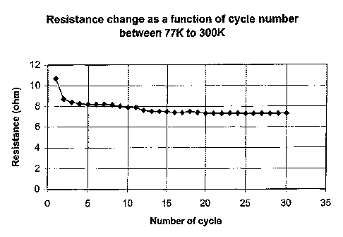
[0021] Fig. 1 is a graph demonstrating the stablilty of resistance in the
heating elettr!ent
of one embodiment of the present invention;

[0022] Flg. 2 is a graph comparing reslstance change in the heating element of
a another
embodiment of the present Invention with that of a heatirrg element In a more
conventional thick film heater; and


CA 02478076 2007-12-05

~ .._ ..- - - - - - , -~-----~--,-, __._~--~~
s

[0023] Fig. 3 Is a graph illustrating the Increasing benefits of the present
inventicsn as
power density (heat flux) increases.

betailed Description

[0024] The present invention is made prlmarily by applying a heating element
of a thick
film resisttve circuit directly to a target objector optlanally over a
dlelectric layer
applled directly to the target object. For the sake of simplicity, the phrase
"directly to
a target obJect" means elther In direct contact with the target owect or In
direct,
contact with a thick film (or thinner) dielectric layer, whlch, In turn, is tn
direct contact
with the target object.

[0025] The application of the heating element to the target object, as well as
the
application of any dielectrlc layers below or above the heating element is
performed
using any of a wide variety of conventional thlck film technologies, such as
screen
printing, all of which are well known in the art. Twa aspects of the present
invention In
tandem distinguish it from the prior art and allow it to achieve the stated
objectlves.

[0026] The first such aspect is the use of specific polymer-based tnks for th@
thick film
circult, such as an epoxy-ba.sed ink. Although other conductive polymer-based
inks
may perform adequately for this Invention, certain polymer-based Inks have
shown
particularly advantageous properties for direct application to a low-
temperature target
object. Ceramlcrbased inks will also work with this invention in some
applications, but
are not preferred due to their higher costs and the inablllty to use them on
non-
ferrous metal substretes. Such preferred polymer-based Inks Include epoxy-
based
inks from Hereaus Company of West Conshohock, P'ennsyivanla and Electro
Science
Laboratories, Inc. of King of Prussia, Pennsyfvanla. At the time of the
present
application, the best known Ink for the present InveMtion is the T2100TM' ink
(epoxq base
with silver conductive particles) on a dielectric layer of,PD5200TM' ink
(epoxy base).
[0027] In low temperature applications, the bindings of silicone-based inks
have become
brlttle during the cooling cycie and chip at the edges. Such chipping produces
resistance changes In the circuit, and could even lead to complete heater
failure
prematurely.

[00281 The second differentlating aspect is the use of addltional curing
cycles or a single


CA 02478076 2004-09-08
WO 03/001849 PCT/US02/19762
6

curing cycle at a higher temperature and/or longer duration than
conventionally used.
The typical directions from the manufacturer for curing the polymer-based inks
in a
thick resistive circuit involve baking the ink at a temperature of 150 C for
thirty
minutes. It has been discovered that such curing cycles do not produce
circuits with
stable resistance. While a circuit cured according to the normal process, as
recommended by the ink manufacturer, might have an initial resistance of 40 S)
for
example, after several thousand heating cycles the resistance will be
permanently
reduced. After as many as 10,000 such cycles, the resistance may be less than
20 S2 -
half of the original resistance. Such permanent changes may not take place in
the
typical thick film application involving a low power density circuit where the
temperature change during a single cycle is not dramatic. This is a major
reason why
thick film circuits are not common place in high power density applications.

[0029] By way of example, a target object of nickel-plated copper was prepared
with a
dielectric paste. The dielectric paste consisted of TiO 2 particle filler and
cobalt oxide
pigment in a polymer-based (epoxy) binding agent. Thinner and thioxtropic
forming
agent were added to the dielectric to make it suitable for deposition using
commonly
known silk screening techniques. The dielectric layer was set in an electric
oven at
temperatures between 50 C and 150 C for a period of sixty minutes.

[0030] Thereafter a thick film resistive circuit was silk screen printed over
the dielectric
layer. The resistive ink was a mixture of silver conducting particles in a
polymer-
based (epoxy) binding agent. Again, thinner and thioxtropic forming agent were
added to thin ink to allow for screen printing. The resistive circuit was
cured
according to manufacturer's specifications - 150 C for thirty minutes. An
outer
dielectric layer identical to the initial dielectric layer was added over the
resistive
circuit. The entire heater (target object, dielectric layers, and resistive
circuit) was
cured for another cycle of 150 C for sixty minutes.

[0031]
The resulting heater was capable of functioning at very low temperatures
without
chipping or cracking. After thirty-five immersions in liquid nitrogen
(temperature:
77K) from room temperature the heating element showed no cracking or
delamination. The resistance of this heater was also stable after fifty such
cycles as
illustrated in Fig. 1. While the low temperature stability of the resistance
was


CA 02478076 2004-09-08
WO 03/001849 PCT/US02/19762
7

excellent, cycling the heating element between 40 C and 125 C resulted in
a
constant decrease in resistance. After 7,000 such heating cycles, the
resistance of the
circuit had decreased approximately 50%.

[0032] It has been discovered that a post curing cycle of 200 C for a longer
period of
time results in more resistance stability at the higher temperature cycling
(40 C 1250
C). Fig. 2 shows the comparative change in resistance over approximately 8,000
such cycles for two heaters prepared as above, but post-cured for three hours
at 150
C and four hours at 200 C. The heaters were designed for 100 watts per
square
inch, but this technology can be used at power densities up to 200 watts per
square
inch.

[0033] The improved stability of the higher temperature post-cure treatments
is more
pronounced at high power densities. Fig. 3 shows the normalized resistance
change
for four heaters prepared as above but with differing post-cure treatments. As
can be
seen, at higher power densities the contrast in resistance stability for the
four heaters
is surprisingly stark. The reason for this dramatic difference is not known,
however
empirical evidence clearly shows the difference is real. It can also be seen
in Fig. 3
that higher temperature in the post-cure treatment are more important than
longer
treatment times. For instance the resistance stability of a post-cure
treatment at 150
C for three hours was dramatically worse than post-cure treatments at 225 C
for two
hours or 200 C for 2.5 hours.

[0034] As mentioned previously, any number of conventional methods may be used
to
deposit the circuit (or dielectric layers) on the target object. For example,
syringe
deposition may be used on target objects that are unsuitable for screen
printing, such
as those with curved geometries. Spraying techniques are also appropriate for
use
with the present invention.

[0035] The heater must of course be terminated, which can also be done with a
wide
variety of known techniques. On appropriate example involves the use of silver
coated
copper lead wires applied onto a terminal pad using the same ink as used for
the thick
film circuit. This is followed by a standard cure treatment (1 50 C for
thirty minutes).
Any number of standard terminating methods may also be used without departing
from the scope of the invention.


CA 02478076 2004-09-08
WO 03/001849 PCT/US02/19762
8

[0036] Accordingly, while this invention is described with reference to a
preferred
embodiment of the invention, it is not intended to be construed in a limiting
sense. It
is rather intended to cover any variations, uses or adaptations in the
invention
utilizing its general principles. Various modifications will be apparent to
persons
skilled in the art upon reference to this description. it is therefore
contemplated that
the appended, and any claims will cover any such modifications or embodiments
as
fall within the true scope of the invention.

Representative Drawing
A single figure which represents the drawing illustrating the invention.
Administrative Status

For a clearer understanding of the status of the application/patent presented on this page, the site Disclaimer , as well as the definitions for Patent , Administrative Status , Maintenance Fee  and Payment History  should be consulted.

Administrative Status

Title Date
Forecasted Issue Date 2009-04-14
(86) PCT Filing Date 2002-06-21
(87) PCT Publication Date 2003-01-03
(85) National Entry 2004-09-08
Examination Requested 2004-09-08
(45) Issued 2009-04-14
Deemed Expired 2020-08-31

Abandonment History

Abandonment Date Reason Reinstatement Date
2007-12-04 R29 - Failure to Respond 2008-02-08
2007-12-04 R30(2) - Failure to Respond 2008-02-08

Payment History

Fee Type Anniversary Year Due Date Amount Paid Paid Date
Request for Examination $800.00 2004-09-08
Reinstatement of rights $200.00 2004-09-08
Application Fee $400.00 2004-09-08
Maintenance Fee - Application - New Act 2 2004-06-21 $100.00 2004-09-08
Registration of a document - section 124 $100.00 2005-03-31
Maintenance Fee - Application - New Act 3 2005-06-21 $100.00 2005-04-07
Maintenance Fee - Application - New Act 4 2006-06-21 $100.00 2006-05-17
Maintenance Fee - Application - New Act 5 2007-06-21 $200.00 2007-06-18
Reinstatement for Section 85 (Foreign Application and Prior Art) $200.00 2008-02-08
Reinstatement - failure to respond to examiners report $200.00 2008-02-08
Maintenance Fee - Application - New Act 6 2008-06-23 $200.00 2008-06-06
Final Fee $300.00 2009-01-16
Maintenance Fee - Patent - New Act 7 2009-06-22 $200.00 2009-05-26
Maintenance Fee - Patent - New Act 8 2010-06-21 $200.00 2010-05-11
Maintenance Fee - Patent - New Act 9 2011-06-21 $200.00 2011-05-11
Maintenance Fee - Patent - New Act 10 2012-06-21 $250.00 2012-05-10
Maintenance Fee - Patent - New Act 11 2013-06-21 $250.00 2013-05-08
Maintenance Fee - Patent - New Act 12 2014-06-23 $250.00 2014-05-15
Maintenance Fee - Patent - New Act 13 2015-06-22 $250.00 2015-05-29
Maintenance Fee - Patent - New Act 14 2016-06-21 $250.00 2016-06-01
Maintenance Fee - Patent - New Act 15 2017-06-21 $450.00 2017-06-19
Maintenance Fee - Patent - New Act 16 2018-06-21 $450.00 2018-06-18
Maintenance Fee - Patent - New Act 17 2019-06-21 $450.00 2019-06-14
Owners on Record

Note: Records showing the ownership history in alphabetical order.

Current Owners on Record
WATLOW ELECTRIC MANUFACTURING COMPANY
Past Owners on Record
LASKOWSKI, THOMAS M.
LIN, HONGY
STEINHAUSER, LOUIS P.
Past Owners that do not appear in the "Owners on Record" listing will appear in other documentation within the application.
Documents

To view selected files, please enter reCAPTCHA code :


To view images, click a link in the Document Description column. To download the documents, select one or more checkboxes in the first column and then click the "Download Selected in PDF format (Zip Archive)" or the "Download Selected as Single PDF" button.

List of published and non-published patent-specific documents on the CPD .

If you have any difficulty accessing content, you can call the Client Service Centre at 1-866-997-1936 or send them an e-mail at CIPO Client Service Centre.


Document
Description 
Date
(yyyy-mm-dd) 
Number of pages   Size of Image (KB) 
Claims 2004-09-08 3 77
Abstract 2004-09-08 2 63
Description 2004-09-08 8 343
Drawings 2004-09-08 2 106
Representative Drawing 2004-09-08 1 7
Cover Page 2004-11-08 1 38
Claims 2007-12-05 7 216
Description 2007-12-05 8 330
Representative Drawing 2009-03-31 1 9
Cover Page 2009-03-31 2 44
Fees 2005-04-07 1 31
PCT 2004-09-08 3 82
Assignment 2004-09-08 4 107
Correspondence 2004-11-04 1 27
Assignment 2005-03-31 4 199
Prosecution-Amendment 2005-05-11 1 29
Prosecution-Amendment 2007-06-04 4 151
Fees 2007-06-18 1 41
Prosecution-Amendment 2007-12-05 15 491
Prosecution-Amendment 2008-02-08 2 65
Fees 2008-06-06 1 41
Correspondence 2009-01-16 2 53