Note: Descriptions are shown in the official language in which they were submitted.
CA 02478238 2004-09-03
WO 03/081291 PCT/US03/08343
TITLE
COMBINATION MICROMACHINE AND OPTICAL DEVICE ARRAY
FIELD OF THE INVENTION
This invention relates to micromachines and, more particularly, micromachines
used
in combination with optical devices such as lasers or photodetectors.
CROSS REFERENCE TO RELATED APPLICATIONS
This application claims priority under 35 USC 119(e)(1) of United States
Provisional
Patent Application Serial No. 60/366,040 filed March 19, 2002.
BACKGROUND OF THE INVENTION
Microelectromechanical devices (MEMS) consist of tiny "micromachines" which
use
electricity to move very small structures. In the optics world, MEMS have been
most widely
used to attempt to make optical cross-connects that use a series of
micromirrors to steer light
from one fiber to another fiber.
FIG. l and FIG. 2 show a MEMS optical cross-connect 100 of the prior art. A
group
of fibers 102, 104, 106, 108 are arranged in an aligned manner so that light
leaving one of the
fibers 108 will traverse an air gap 110 and enter another fiber 104 aligned
with the first fiber
108. Similarly, light from a different fiber 106 exiting the fiber 106 will
enter a different
fiber 102 aligned with it. A MEMS micromirror 112 that is moveable into and
out of the air
gap 110 is also provided. The movement of the micromirror 112 into and out of
the air gap
110 affects where light exiting a fiber into the air gap 110 goes and thus,
can be used to steer
light exiting a fiber to different fibers depending upon the micromirror's 112
position. For
example, when the micromirror 112 is not in the air gap 110, i.e. in the
position shown in
FIG. 1, the light travels straight through the air gap 110. However, when the
micromirror 112
is moved into the air gap 110, as is shown in FIG. 2, the light will be
steered to an adjacent
fiber. In other words, light leaving one of the fibers 106 when the
micromirror 112 is in the
position of FIG. 1 will enter the fiber 102 directly across from it. Whereas,
with the
miocromirror 112 in the position of FIG. 2, light leaving the same fiber 106
will be steered to
a different fiber 104.
Presently however, to the extent such micromachine cross-connects even exist,
their
use is limited and they are configured as stand alone elements.
CA 02478238 2004-09-03
WO 03/081291 PCT/US03/08343
Thus, there is a need in the art for more versatile MEMS devices that can be
more
easily used in conjunction with active optical devices.
SUMMARY OF THE INVENTION
We have conceived of MEMS devices and arrangements that make it possible to
combine electronics, active optical devices and micromachine based passive
optical devices
in a way that makes them more versatile and more closely coupled with active
optical
devices.
The advantages and features described herein are a few of the many advantages
and
features available from representative embodiments and are presented only to
assist in
understanding the invention. It should be understood that they are not to be
considered
limitations on the invention as defined by the claims, or limitations on
equivalents to the
claims. For instance, some of these advantages are mutually contradictory, in
that they cannot
be simultaneously present in a single embodiment. Similarly, some advantages
are applicable
to one aspect of the invention, and inapplicable to others. Thus, this summary
of features and
advantages should not be considered dispositive in determining equivalence.
Additional
features and advantages of the invention will become apparent in the following
description,
from the drawings, and from the claims.
BRIEF DESCRIPTION OF THE DRAWINGS
FIG. 1 is a MEMS optical cross-connect of the prior art with its mirror in one
position;
FIG. 2 is a MEMS optical cross-connect of the prior art with its mirror in an
alternative position;
FIG. 3 is a simplified representative example of one variant unit according to
the
teachings of the invention;
FIG. 4A shows a single device from the example of FIG. Sin a neutral position;
FIG. 4B shows the lens of FIG. 4A after it has been moved along the y-axis;
FIG. 4C is the device of FIG. 4A after it has been moved along the x-axis;
FIG. 5 is a tilting MEMS micromirror suitable for use in connection with
various
implementations of the invention;
FIG. 6 is a simplified representative example of another variant unit
according to the
teachings of the invention;
-2-
CA 02478238 2004-09-03
WO 03/081291 PCT/US03/08343
FIG. 7A shows one device from the example of FIG. Gin one micromirror 608
position;
FIG. 7B, shows the micromirror 608 of FIG. 7A after it has been pivoted about
its
pins to one position;
FIG. 7C is the device of FIG. 7A after it has been pivoted about its pins to
another
position;
FIG. 8A is a further example of one passive device for use with a single
active device
in accordance with the teachings of the present invention;
FIG. 8B shows the device of FIG. 8A in one position;
FIG. 8C shows the device of Fig. 8A in another position;
FIG. 9A is a further example of one passive device for use with a single
active device
in accordance with the teachings of the present invention;
FIG. 9B shows the device of FIG. 9A in one position;
FIG. 9C shows the device of Fig. 9A in another position;
FIG. 10 shows, in simplified overview, the process of making an array in
accordance
with the invention;
FIG. 11 is a cutaway side view of a plane moveable lens based unit
implementing the
teachings of the invention;
FIG. 12 shows the final unit of FIG. 11 after the MEMS lens has been
integrated with
the IC 1104;
FIG. 13 is a cutaway side view of a pivoting MEMS micromirror that can also be
integrated with the active optical device and IC of FIG. 11;
FIG. 14 shows the final unit of FIG. 13 after the MEMS micromirror has been
integrated with the IC;
FIG. 15 shows yet another example of a MEMS device that can be integrated with
an
active optical device in accordance with the teaclungs of the invention; and
FIG. 16 shows still another example of a MEMS device that can be integrated
with an
active optical device in accordance with the teachings of the invention.
DETAILED DESCRIPTION
This invention relates to the integration of arrays micromachines (movable
lenses and
mirrors) on top of integrated arrays of photonic devices (lasers, detectors,
and/or modulators)
that are themselves closely integrated with, typically on top of, electronic
chips.
-3-
CA 02478238 2004-09-03
WO 03/081291 PCT/US03/08343
There are two main classes of optical devices: active and passive. Active
optical
devices are devices which, through the use of external power sources and
materials, change a
behavior of light. Examples of active optical devices are lasers, detectors,
and modulators.
Passive optical devices are devices in which no external power is used to
modify light
behavior. Instead the interaction of the light with the material of the device
itself is used to
effect a change in the light's behavior. Examples of passive optical devices
are lenses,
mirrors and waveguides.
While passive optical devices do not use power to change the behavior of the
light, by
moving a passive optical element relative, the way light interacts with it can
be changed. For
example, if a mirror is moved by tilting, the effect resulting from light's
interaction with the
mirror will be different, because it may be reflected at a different angle. If
the mirror is
flexible, changing the mirror from a flat plane to a curved one can cause the
way light
interacts with the mirror to change.
Similarly, the interaction of light with a particular lens will be different,
depending
upon where on the lens the light strikes.
As a result, by making passive optical MEMS devices, where the passive device
is
moveable, and closely integrating those devices with active optical devices,
highly versatile
and beneficial results can be achieved.
In accordance with the invention, depending upon the particular
implementation, the
passive optical device can be made so that it is moveable: in a plane
essentially perpendicular
to the direction light is emitted/received by an active optical device, in a
tilting fashion
relative to the direction light is emitted/received by an active optical
device, along the
direction light is emitted/received by an active optical device, or some
combination thereof.
FIG. 3 is a simplified representative example of one variant unit 300
according to the
teachings of the invention. In this example, the unit 300 is made up of
multiple active optical
devices 302, in this case lasers, integrated with an electronic integrated
circuit (IC) chip 304
to form an opto-electronic chip. An array of lenses 306 is located above the
active optical
devices 302. Each lens 308 is individually moveable, in this case in the x-y
plane (i.e. a plane
essentially perpendicular to the direction the laser emits). By moving the
lens, along the x-
axis, the y-axis or both axes, the optical beams from the laser can be
"steered". This makes it
possible to couple the light from a single laser to two or more different
fibers.
FIG. 4A shows a single device from the example of FIG. Sin a neutral position.
In
this position, the emitted light travels along the z-axis.
-4-
CA 02478238 2004-09-03
WO 03/081291 PCT/US03/08343
FIG. 4B shows the lens of FIG. 4A after it has been moved along the y-axis to
a
position such that the emitted light from the laser is steered along the y-z
plane.
FIG. 4C is the device of FIG. 4A after it has been moved along the x-axis to a
position
such that the emitted light from the laser is steered along the x-z plane.
Of course, by using a combination of movement in both the x and y direction,
the
beam can be steered towards a different location between the directions of
FIG. 4B and FIG.
4C. Similarly, movement in the minus x or minus y directions will produce
analogous
results.
FIG. 5 is a tilting MEMS micromirror 500 suitable for use in connection with
various
implementations of the invention. The micromirror 500 has two pins 502 at
opposite corners
of the micromirror 500 (the micromirror in this case being square in shape,
although
rectangles, ovals, circles, etc. could be used in different implementations).
A portion 504 of
the micromirror 500 contains a charge (electrical or magnetic) so that the
application of a
micro-electric field, for example, from an electrically or electro-statically
charged plate, pad
or coil 506 will cause the portion 504 to be attracted to or repelled by the
field, thereby
pivoting the micromirror 500 about the pins 502. Optionally, as will be
described in greater
detail below, a hole 508 can be included in the micromirror 500 so that,
depending upon the
size of the hole 508 and its placement on the mirror, different effects can be
achieved.
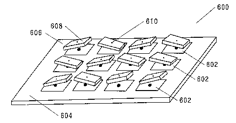
FIG. 6 is a simplified representative example of another variant unit 600
according to
the teachings of the invention. In this example, the unit 600 is made up of
multiple active
optical devices 602, in this case detectors, integrated with an electronic
integrated circuit (IC)
chip 604 to form an opto-electronic chip. An array 606 of pivotable
micromirrors 608 is
located above the active optical devices 602. Each micromirror 608 is
individually tilt-able
about pins (not shown). By pivoting a micromirror 608, about the pins, optical
beams can be
steered by reflection in different directions. In addition, an optional hole
610 placed in the
mirror allows light to reach the detector 602 located below a micromirror 608.
Depending
upon the size and placement of the hole 610, a small amount of light can
strike the detector
while the bulk is reflected, most or all of the light can reach a detector
602, or all of the light
can be reflected.
Advantageously, this allows some variants to operate so that a micromirror 608
can steer
external light while the detector 602 below detects some of the light and
switches the mirror
based upon information in the light stream.
-5-
CA 02478238 2004-09-03
WO 03/081291 PCT/US03/08343
FIG. 7A shows one device from the example of FIG. Gin one micromirror 608
position. In this position, the incident light is reflected towards the left.
FIG. 7B, shows the micromirror 608 of FIG. 7A after it has been pivoted about
its
pins such that the incident light is reflected towards the right.
FIG. 7C is the device of FIG. 7A after it has been pivoted such that some of
the
incident light passes through the hole 610 to the detector 602 below while the
remainder of
the incident light is reflected.
FIG. 8A is a fiuther example of one passive device 800 for use with a single
active
device in accordance with the teachings of the present invention. In this
example, the passive
800 is optically opaque and has a hole 802 that is offset from its center. The
passive device
800 is designed to be moved in the x-y plane, similar to the lenses of FIG. 3
or FIG. 4. By
placing this device 800 over a laser, the laser can be left in a continuous
emitting or "on"
state and, depending upon the position of the device 800, the emitted beam
will either pass
through the hole 802 (FIG. 8B) or be blocked by the device 800 (FIG. 8C). In
this manner,
the device can be used, for example, as a switch.
Depending upon the particular implementation, it should be understood that the
device 800 can be a reflective material or a material that absorbs light.
FIG. 9A is another example of a passive device 900 for use with a single
active device
in accordance with the teachings of the present invention. In this example,
the passive 900 is
optically opaque and has a hole 902 that is offset from its center. The
passive device 900 is
designed to pivot about pins 904, similar to the micromirrors of FIG. 5, FIG.
6 or FIG. 7. By
placing this device 800 over a laser, the laser can be left in a continuous
emitting or "on"
state and, depending upon the position of the device 900, the emitted beam
will either pass
through the hole 902 (FIG. 9B) or, if the material making up the device 900 is
reflective, the
emitted beam can be directed to another location, for example a fiber, another
passive device,
or a nearby detector. If the material is light absorbing, the emitted beam
will be blocked by
the device 800. In this manner, the device can be used both to steer a beam
and as a switch.
Moreover, if the material is reflective in one area while being light
absorbing in another,
further combinations can be achieved.
FIG. 10 shows, in simplified overview, the process of making an array in
accordance
with the invention, looking perpendicular to the plane of the devices. First
an IC 1002 has
the array of active devices 1004 attached to it. Depending upon the particular
implementation, this can be accomplished using techniques well known in the
art or
-6-
CA 02478238 2004-09-03
WO 03/081291 PCT/US03/08343
techniques such as shown and described in commonly assigned U.S. Patent
Application Nos.
09/896,189, 091896,665, 09/897,160, 09/896,983, 09/897,158, all filed June 29,
2001, the
entire disclosures of which are incorporated herein by reference. Then, the
array of MEMS
devices 1006 are attached over the active devices. In alternative variants,
the optical devices
1004 can be integrated with the MEMS devices 1006 before they are integrated
with the IC
1002.
As shown, the MEMS devices are lenses 1008 that are each moveable in the x-y
plane
by fields generated along the x axis by a pair of elements 1010 that push-pull
the lens 1008
along the x-axis and a pair of elements 1012 that push-pull the lens 1008
along the y-axis.
FIG. 11 is a cutaway side view of a plane moveable lens based unit
implementing the
teachings of the invention. An active optical device 1102, in this case a
laser, is mounted
onto an electronic IC 1104. The IC 1104 includes circuitry to control both the
data output by
the laser, and also the position of the lens 1106 using steering input X 1108
and steering input
Y. The MEMS lens 1106 is placed over the active device 1102 and will be
connected to the
steering inputs 1108, 1110 of the IC 1104 via connection pads 1112. FIG. 12
shows the final
unit 1200 after the MEMS lens 1106 has been integrated with the IC 1104.
FIG. 13 is a cutaway side view of a pivoting MEMS micromirror 1302 that can
also
be integrated with an active optical device 1300, in this case a photodetector
1300, and the IC
1104 of FIG. 11. As shown, the micromirror 1302 includes a mirror element 1304
that has a
hole 1306 in it so that light can be steered by pivoting the mirror while a
small amount of
incident light will pass through to the photodetector 1300, irrespective of
the position of the
mirror element 1304.
FIG. 14 shows the final unit 1400 after the MEMS micromirror 1302 has been
integrated with the IC 1104.
FIG. 15 shows yet another example of a MEMS device that can be integrated with
an
active optical device in accordance with the teachings of the invention. In
the example of
FIG. 15, a flexible reflective element 1500 is constrained on one side 1502,
for example by
fixed pins 1504. A pair of slideably moveable pins 1506 allow the curvature of
the element
1500 to be changed, for example from nearly flat to highly curved, thereby
deflecting
incident light on the element 1500 differently based upon the angle of the
incident light, the
curvature of the element 1500, and location the light strikes the element
1500.
FIG. 16 shows still another example of a MEMS device that can be integrated
with an
active optical device in accordance with the teachings of the invention. In
the example of
_7_
CA 02478238 2004-09-03
WO 03/081291 PCT/US03/08343
FIG. 16, a flexible reflective element 1600 has a pair of slideably moveable
pins 1602, 1604
on either side of the element 1600 that allows the curvature of the element
1600 to be
changed, for example from concave to convex, thereby deflecting incident light
on the
element 1600 differently based upon the angle of the incident light, the
curvature of the
element 1600, and location the light strikes the element 1600.
It should be understood that the above description is only representative of
illustrative
embodiments. For the convenience of the reader, the above description has
focused on a
representative sample of all possible embodiments, a sample that teaches the
principles of the
invention. The description has not attempted to exhaustively enumerate all
possible
variations. That alternate embodiments may not have been presented for a
specific portion of
the invention, or that further undescribed alternate embodiments may be
available for a
portion, is not to be considered a disclaimer of those alternate embodiments.
One of ordinary
skill will appreciate that many of those undescribed embodiments incorporate
the same
principles of the invention and others are equivalent.
_g_