Note: Descriptions are shown in the official language in which they were submitted.
CA 02479024 2004-09-13
WO 03/081687 PCT/US03/07269
SELF-ALIGNED NANOTUBE FIELD EFFECT TRANSISTOR AND
METHOD OF FABRICATING SAME
BACKGROUND OF THE INVENTION
1. Field of the Invention
The present invention relates to field effect
transistors, and more particularly, to carbon-nanotube field
effect transistors.
2. Discussion of the Related Art
In the field of molecular nanoelectronics, few materials
show as much promise as nanotubes, and in particular carbon
nanotubes, which comprise hollow cylinders of graphite,
angstroms in diameter. Nanotubes can be implemented in
electronic devices such as diodes and transistors, depending
on the nanotube's electrical characteristics. Nanotubes are
unique for their size, shape, and physical properties.
Structurally a carbon-nanotube resembles a hexagonal lattice
of carbon rolled into a cylinder.
Besides exhibiting intriguing quantum behaviors at low
temperature, carbon nanotubes exhibit at least two important
characteristics: a nanotube can be either metallic or
semiconductor depending on its chirality (i.e., conformational
geometry). Metallic nanotubes can carry extremely large
current densities with constant resistivity. Semiconducting
nanotubes can be electrically switched on and off as
field-effect transistors (FETs). The two types may be
covalently joined (sharing electrons). These characteristics
CA 02479024 2004-09-13
WO 03/081687 PCT/US03/07269
2
point to nanotubes as excellent materials for making
nanometer-sized semiconductor circuits.
In addition, carbon nanotubes are one-dimensional
electrical conductors, meaning that only one-dimensional
quantum mechanical mode carries the current. This can be a
significant advantage with respect to the device performance
of a carbon-nanotube based transistor since scattering in the
material is significantly suppressed. Less scattering means a
better performance of the device.
For a three terminal device, such as an FET, a gate (the
third terminal) needs to be isolated from the electrically
active channel region as well as a source and a drain. For
this purpose a dielectric material, e.g., silicon dioxide can
be used. To improve device characteristics in silicon devices,
the thickness of this layer can be reduced. This reduction
increases the gate capacitance and improves the
gate-to-channel coupling. For standard silicon field-effect
devices the gate capacitance scales inversely proportional to
the dielectric film thickness. For currently manufactured
high-performance processors, the Si02 thickness is less than
4nm. Significantly, further reduction can be difficult to
achieve since gate leakage through the dielectric film
increases exponentially for an oxide thickness below 4nm.
However, the gate capacitance for a carbon-nanotube
transistor does not scale inversely proportional with the
dielectric film thickness. Instead, carbon-nanotubes follow a
logarithmic scaling law. In comparison with a standard silicon
CA 02479024 2004-09-13
WO 03/081687 PCT/US03/07269
3
field-effect transistor, the gate capacitance for a
carbon-nanotube transistor can be larger because of the
cylindrical geometry of these objects.
No known system or method has implemented a nanotube to
achieve performance and smaller sire in an FET. Therefore, a
need exists for a system and method of preparing nanotube
based FETs.
SU'N~2ARY OF THE INVENTION
According to an embodiment of the present invention, a
self-aligned carbon-nanotube field effect transistor
semiconductor device is provided. The device comprises a
carbon-nanotube deposited on a substrate, a source and a drain
formed at a first end and a second end of the carbon-nanotube,
respectively, and a gate formed substantially over a portion
of the carbon-nanotube, separated from the carbon-nanotube by
a dielectric film.
The substrate comprises a thermal oxide deposited over a
silicon substrate. The thermal oxide is about 150 nanometers
thick.
The gate is further separated from the carbon-nanotube by
an oxide layer. A portion of the gate is separated from the
source and the drain by a nitride spacer.
The device further comprises a passivation dielectric
layer over the device.
,The device comprises an alignment mark in the substrate
to which the source and the drain are aligned.
CA 02479024 2004-09-13
WO 03/081687 PCT/US03/07269
4
The gate wraps around the dielectric film and the
carbon-nanotube to contact a back side of the carbon-nanotube.
According to an embodiment of the present invention, a
carbon-nanotube field effect transistor semiconductor device
is provided. The device comprises a vertical carbon-nanotube
wrapped in a dielectric material, a source and a drain formed
on a. first side and a second side of the carbon-nanotube,
respectively, a bilayer nitride complex through which a band
strap of each of the source and the drain is formed connecting
IO the carbon-nanotube wrapped in the dielectric material to the
source and the drain, and a gate formed substantially over a
portion of the carbon-nanotube.
The device comprises a metal catalyst at a base of the
carbon-nanotube.
IS According to one embodiment of the present invention, a
method is provided for forming a self-aligned carbon-nanotube
field effect transistor semiconductor device. The method
comprises depositing a nanotube on a thermal oxide substrate,
wherein the substrate includes an alignment mark, forming a
20 metal contact at each end of the nanotube, wherein a first
metal contact is a source and a second metal contact is a
drain, and depositing an amorphous silicon layer over the
device. The method further comprises forming nitride spacers
on opposing sides of each metal contact,depositing a high k
25 dielectric film aver the device, oxidizing the amorphous
silicon, and forming a gate substantially between the source
and the drain, and over the nanotube.
CA 02479024 2004-09-13
WO 03/081687 PCT/US03/07269
The method comprises depositing a passivation dielectric
over the device.
The nanotube is a single-walled nanotube. The metal
contacts are formed using a photoresist.
5 According to an embodiment of the present invention, a
method is provided for forming a self-aligned carbon-nanotube
field effect transistor semiconductor device. The method
comprises depositing a nanotube on a thermal oxide substrate,
wherein the substrate includes an alignment mark, forming a
metal contact by reactive ion etch at each end of the
nanotube, wherein a first metal contact is a source and a
second metal contact is a drain, and forming nitride spacers
on opposing sides of each metal contact. The method further
comprises depositing a high k dielectric film over the device,
and forming a gate substantially between the source and the
drain and over the nanotube.
The method comprises depositing a passivation dielectric
over the device.
.According to an embodiment of the present invention, a
method is provided for forming a self-aligned carbon-nanotube
field effect transistor semiconductor device. The method
comprises depositing a nanotube on a thermal oxide substrate,
wherein the substrate includes an alignment mark, and forming
an amorphous silicon pillar over each end of the nanotube. The
method further comprises isolating the amorphous silicon
pillars with a layer of oxide, forming a gate dielectric layer
between amorphous silicon pillars, and forming a gate
CA 02479024 2004-09-13
WO 03/081687 PCT/US03/07269
6
substantially between the amorphous silicon pillars and over
the nanotube. The method comprises forming a nitride layer
over the gate, forming oxide spacers on each side of the gate,
replacing the amorphous silicon with metal contacts, wherein a
first metal contact is a source and a second metal contact is
a drain, and depositing a passivation dielectric over the
device.
According to another embodiment of the present invention,
a method is provided for forming a self-aligned
carbon-nanotube field effect transistor semiconductor device.
The method comprises . depositing a metal catalyst on a
thermal oxide substrate, depositing a low temperature oxide
layer over the device, etching a trench through the oxide, the
metal catalyst and into a thermal oxide underlying the metal
catalyst, and etching the low temperature oxide layer to form
oxide islands. The method further comprises stripping exposed
metal Catalyst, growing a nanotube between metal catalyst
beneath the oxide islands, and wrapping the nanotube in a gate
dielectric. The method comprises forming nitride spacers on
the opposing surfaces of the oxide islands, forming a gate
substantially between the oxide islands by chemical vapor
deposition and over the nanotube, and depositing a passivation
dielectric over the device.
According to an embodiment of the present invention, a
method is provided for forming a self-aligned carbon-nanotube
field effect transistor semiconductor device. The method
comprises growing a nanotube vertically from a metal catalyst
CA 02479024 2004-09-13
WO 03/081687 PCT/US03/07269
7
forming on a surface of the semiconductor device, forming a
nitride block structure, and wrapping the nanotube in a gate
dielectric. The method comprises depositing a gate metal
separated from the metal catalyst by the dielectric layer,
depositing a nitride layer, and forming gate metal pillars
capped with the nitride layer. The method forms nitride
spacers around the pillars, deposits a drain metal
substantially between the pillars Separated from the gate
metal by the dielectric layer, and deposits a passivation
dielectric over the device.
BRIEF DESCRIPTION OF THE DRAWINGS
Preferred embodiments of the present invention will be
described below in more detail, with reference to the
accompanying drawings:
Figs. 1a-i illustrate a source/drain first
carbon-nanotube field effect transistor according to an
embodiment of the present invention;
Figs. 2a-b illustrate another source/drain first
carbon-nanotube field effect transistor according to an
embodiment of the present invention;
Figs. 3a-g illustrate a gate first carbon-nanotube field
effect transistor according to an embodiment of the present
invention;
Figs. 4a-d illustrate a Carbon-nanotube field effect
transistor comprising a nanotube grown in place according to
an embodiment of the present invention;
CA 02479024 2004-09-13
WO 03/081687 PCT/US03/07269
Figs. 5a-n illustrate a carbon-nanotube field effect
transistor comprising a nanotube grown in place vertically
according to an embodiment of the present inventionp and
Figs. 6a-b illustrate directed assembly of nanotubes
according to an embodiment of the present invention.
DETAINED DESCRIPTION Of PREFERRED EMBODIMENTS
According to an embodiment of the present invention, a
gate, a source and a drain of a field effect transistor (FET)
are self-aligned, thereby reducing overlap capacitances.
According to an embodiment of the present invention, a
carbon-nanotube FET can be fabricated using a pattern transfer
by lift-off etch, wherein the source and the drain are formed
before the gate. Referring to Figs. 1a-i, an alignment mark
101 is formed in a thermal oxide 102 and silicon substrate
103. The alignment mark 101 is a high precision feature that
can be used as a reference when positioning patterns. The
thermal oxide 102 is deposited over the silicon 103, The
silicon can be, for example, P+ doped (0.0152-cm, about
3x10¹⁸crri 3) . A nanotube 104 can be deposited on the thermal
oxide 102 and a photoresist 105 can be positioned by
photolithography. The nanotube can be deposited in the form of
a slurry, where nanotube deposition is random. The nanotube
can be deposited by directed assembly, as described below. The
photoresist exposes the ends of the nanotube. Metal contacts
106-107 are formed in the trenches that expose the nanotube
ends. The metal can be, for example, Cobalt (Co), Nickel (Ni),
CA 02479024 2004-09-13
WO 03/081687 PCT/US03/07269
9
Tungsten (W), or Titanium (Ti?. The metal can be deposited
over the device, filling the trenches exposing the ends of the
nanotube 104. The photoresist 105 can be stripped. The metal
deposited in the trenches form source/drain contacts 106-107.
An amorphous Silicon (a-Si) 108 can be deposited over the
device. A Nitride layer 109 Can be deposited over the a-Si
layer. The Nitride can be etched to form spacers, e.g., 110 on
the sides of the metal contacts 106-107. The amorphous silicon
108 can be selectively removed or wet chemically oxidized. A
gate dielectric film 111 can be deposited over the device.
Here as in the following methods, the dielectric can be
silicon dioxide as well as any other high-k dielectric
material, for example, HfOz. A gate 112 can be formed
substantially between the metal contacts 106-107 forming the
source and drain, for example by CVD and etching. A
passivation dielectric layer 113 is deposited over the device.
The source, drain and gate 112 are self-aligned to the
alignment mark 101.
Alternatively, the source/drain can be formed before the
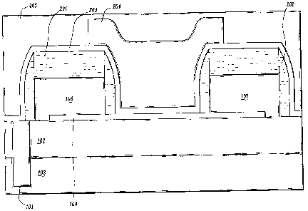
gate with a reactive ion etch (RIE). Referring to Figs. 2a-b,
a method forms the source/drain, 106-107, first using RIE to
define the source/drain metal. The RIE needs to be isolated
from the carbon-nanotube 104. A nitride layer 201 can be
deposited over the device and etched from the areas
surrounding the metal contact. Nitride spacers, e.g., 202, can
be formed on the sides of the metal contacts. A gate
dielectric 203 is deposited over the device. The gate metal
CA 02479024 2004-09-13
WO 03/081687 PCT/US03/07269
204 is formed substantially between the source and the drain,
106-107. A passivatlon dielectric 205 can be deposited over
the device. The thermal oxide can be approximately 150nm
thick.
5 According to another embodiment of the present invention,
the gate can be formed before the source/drain. Amorphous
silicon 301 can be deposited over the ends of the nanotube
104. The a-Si can be covered with an oxide layer 302. A gate
dielectric 303 can be deposited between the a-Si, e.g., 301. A
10 gate 304 can be formed substantially between the a-Si pillars,
e.g., 301. A nitride layer 305 can be formed over the gate
metal 304. Oxide spacers, e.g., 306 can be formed on the ends
of the gate metal 304. The exposed corners of the a-Si/oxide
can be stripped, exposing the a-Si. The remaining a-Si
surrounding the gate metal can be removed by RIE. Metal
contacts 307-308 can be deposited in the area previously
occupied by the a-Si, The metal contacts 307-30S are connected
to the nanotube 104 that runs beneath the gate dielectric 303
and gate metal 304. The metal contacts 307-308 form the source
and the drain of. the device. The metal contacts 307-308 can be
aligned to the alignment mark 101 deposited in the thermal
oxide 102 and silicon 103 substrate. A passivation dielectric
309 can be deposited over the device.
According to an embodiment of the present invention, a
carbon-nanotube FET can be grown in place. The source/drain
can be formed before the gate. An amorphous silicon layer 401
is deposited over the thermal oxide layer 102. A low
CA 02479024 2004-09-13
WO 03/081687 PCT/US03/07269
11
temperature oxide (LTO) layer 402 can be deposited over the
metal catalyst. A trench can be etched from the oxide 402,
amorphous silicon 401 and thermal oxide 102. The amorphous
silicon 401 can be partially under cut from below the oxide
402. A metal catalyst 401B, for example, Fe, Co, Ni or Fe/Mo
can be self-assembled on the edges of the undercut amorphous
silicon film 401. The carbon-nanotube 403 can be grown between
the remaining portions of the metal catalyst 401B, wherein a
portion of the nanotube is suspended over the thermal oxide
102. A gate dielectric film 404 can be deposited by chemical
vapor deposition (CVD), wrapping the nanotube 403. Thus, the
nanotube 403 can be completely covered with the gate
dielectric, e.g., SiO~. Spacers, e.g., 405, can be formed on
the sides of the oxide, e.g., 402. A gate 406 can be formed
substantially between the oxide, e.g., 402. If the etch in the
thermal oxide 102 is sufficiently deep, the gate metal 406 Can
surround the whole nanotube 403 and the dielectric film 404
stack. For this purpose the gate metal can be deposited by
means of chemical vapor deposition to cover the back side of
the nanotube/dielectric film stack. The wrapped around
configuration offers a good gate-to-nanotube coupling. A
passivation dielectric 406 can be deposited over the surface
of the device.
According to another embodiment of the present invention,
a carbon-nanotube can be grown in place vertically. The
nanotube can be grown vertically from, for example, a metal
source at the base or a metal particle catalyst. Referring to
CA 02479024 2004-09-13
WO 03/081687 PCT/US03/07269
12
Fig. 5a-n, a metal catalyst 501 can be formed on the silicon
substrate 502. A first layer of Nitride 503 can be deposited
over.the device. An oxide layer 504 Can be deposited over the
first Layer of Nitride 503. A second layer of Nitride 505 can
be deposited over the oxide 504. A photoresist, e.g., 506, can
be formed on the device by photolithography, wherein the metal
catalyst 501 is exposed. A plurality of second metal
catalysts, e.g., 507, are deposited over the device. The
photoresist, e.g., 506, can stripped, such that the second
catalyst, e.g., 507, formed on the first metal catalyst 501
remain. From each second metal catalyst, e.g., 507, a
nanotube, e.g., 508, can be grown vertically. Thus,
two-dimensional and three-dimensional arrays of nanotubes can
be formed.
Vertical growth of the nanotubes occurs when the metal
particle catalyst is placed in a pore aligned vertically to
the substrate. In this case, the space for the growth is
confined and forces the growth of the tube to follow the
vertical direction. Tn principle, vertical pores such as in
Fig.~5b can be made using the resists arid pattern transfer.
An amorphous Silicon layer 509 can be deposited over the
device. The device can be planarized down to the second
Nitride layer 505. A portion of the Nitride-Oxide-Nitride
layering, 503-505, can be removed from the device. A pillar
surrounding the nanotubes, e.g., 508, and metal catalyst, 501
and 507, remains. A sacrificial layer 510 can be formed over
the Nitride layer 505 the nanotubes 508 and the a-Si 509. 'The
CA 02479024 2004-09-13
WO 03/081687 PCT/US03/07269
13
contact layer can be, for example, titanium or tungsten. The
oxide layer 504 can be removed from between the layers of
Nitride, 503 and 505. The a-Si 509 can be etched
simultaneously with the oxide layer 504 from around the
nanotubes, e.g., 508, Alternatively, the a-So 509 can be
removed after the oxide layer 504 has been removed. A gate
dielectric, e.g., 511, can be formed around the nanotubes,
e.g., 508, over the metal catalyst 501 and under the
sacrificial layer 510. Alternatively, fox a two-dimensional
IO array of nanotubes, the gate dielectric 511 can be deposited
between the nanotubes, The sacrificial Payer 510 can be
removed, for example, by an etch. The gate metal 512 can be
deposited over the surface of the device. A third Nitride
layer 513 can be deposited over the gate metal 512. Portions
of the gate metal 512 and the third nitride layer 513 can be
removed. Pillars of gate metal and nitride spacers, e.g., 512
and 513, remain around the metal catalyst-nanotube structure.
Nitride spacers, e.g., 51.4, are formed around each pillar. A
drain 515 can be .formed over the metal catalyst-nanotube
structure, forming a FET. The passivation dielectric 516 can
be deposited between FETs.
Tt should be noted that the exact mechanics of nanotube
growth from a metal catalyst are not known. However, the
process of growing a single-walled nanotube from a metal
catalyst, for example, Cobalt (CO) over alumina-supported
Molybdenum (Mo) particles, can be implemented in a number of
ways:
CA 02479024 2004-09-13
WO 03/081687 PCT/US03/07269
14
According to an embodiment of the present invention,
nanotubes can be put in place by a method of directed assembly
rather than deposited or grown as described above. Directed
assembly can be used for horizontal and vertical deposition of
a nanotube using selective deposition driven by a chemical or
a physical process. The selective deposition can include
forming an adhesion layer or chemical groups acting as
receptors to favor a desired deposition of tubes in a given
position. Figs. 6a and 6b show methods for horizontal and
vertical directed assembly. respectively. A nanotube 601 can
be prepared comprising predetermined chemical groups 602, for
example, a DNA strand or a thiol group, at each end. The
nanotube 601 can be brought into the proximity of a substrate
603 comprising receptors 604, for example, where DNA is
implemented, a complementary DNA strand can be used. Where a
thiol group is used, gold particles or a contact shape
comprising gold, can be designed to bond with the chemical
groups 602 of the nanotube 601. The nanotube 601 can thus be
placed on the substrate 603 according to directed assembly.
For improved performance high-K dielectric films, those
having a high dielectric constant, can be used as gate
insulators. The capacitance of a carbon-nanotube FET does not
significantly change as a function of the thickness of the
dielectric film, thus, it can be difficult to achieve the
desired capacitance, even with thin gate dielectric films.
Aluminum oxide A1203 (k = 9) as well as Hafnium oxide (Hf02) (k
- 20) are promising candidates in this context. CVD-aluminum
CA 02479024 2004-09-13
WO 03/081687 PCT/US03/07269
1$
Can be oxidized to generate a high-K gate dielectric or
CVD-A1203(Hf02 can be deposited directly. Compared with Si02,
these materials increase the gate capacitance by a factor of
up to five, and can have a larger impact on the device
performance than reducing the dielectric film thickness. Since
nanotubes are pFETs in an air environment and become nFETs in
vacuum and inert gases like Argon (Ar) after annealing, the
device can be annealed before the deposition of the dielectric
film is added. This converts the tubes into nFETs. Capping
them in situ with the dielectric also prevents tubes from
becoming pFETs again. For a complementary technology the
dielectric film on FETS, which should be turned into pFETs,
can be locally removed - also allowing the FETs to be doped. A
CVD deposition at low temperature coats these devices again
(without an extra annealing step before).
Since all structures (pFETs and nFETs) are covered with
oxide (or any other suitable dielectric film) no short is
generated when the gate electrode is fabricated. CVD can be
used~for the deposition of the gate. Using chemical vapor
deposition for fabrication schemes as described in Figs. 4 and
5 can ensure that nanotubes that are already wrapped in a
dielectric film become completely surrounded by the metal
gate. This can be important for good gate-to-nanotube
coupling. The gate metal can be patterned and removed where
desired. Source and drain electrodes can be opened for
electrical access.
CA 02479024 2004-09-13
WO 03/081687 PCT/US03/07269
16
Having described preferred embodiments for
carbon-nanotube FETs and methods of making same, it is noted
that modifications and variations can be made by persons
skilled in the art in light of the above teachings. It is
therefore to be understood that changes may be made in the
particular embodiments of the invention disclosed which are
within the scope and spirit of the invention as defined by the
appended claims. Having thus described the invention with the
details and particularity required by the patent laws, what is
claimed and desired. protected by Letters Patent is set forth
in the appended claims.