Language selection

Search

Patent 2479397 Summary

Third-party information liability

Some of the information on this Web page has been provided by external sources. The Government of Canada is not responsible for the accuracy, reliability or currency of the information supplied by external sources. Users wishing to rely upon this information should consult directly with the source of the information. Content provided by external sources is not subject to official languages, privacy and accessibility requirements.

Claims and Abstract availability

Any discrepancies in the text and image of the Claims and Abstract are due to differing posting times. Text of the Claims and Abstract are posted:

  • At the time the application is open to public inspection;
  • At the time of issue of the patent (grant).
(12) Patent Application: (11) CA 2479397
(54) English Title: ELECTRO-ABSORPTION MODULATOR WITH BROAD OPTICAL BANDWIDTH
(54) French Title: MODULATEUR A ELECTRO-ABSORPTION A GRANDE LARGEUR DE BANDE OPTIQUE
Status: Deemed Abandoned and Beyond the Period of Reinstatement - Pending Response to Notice of Disregarded Communication
Bibliographic Data
(51) International Patent Classification (IPC):
  • G02F 1/017 (2006.01)
  • G02F 1/015 (2006.01)
(72) Inventors :
  • MARSH, JOHN HAIG (United Kingdom)
(73) Owners :
  • INTENSE LIMITED
(71) Applicants :
  • INTENSE PHOTONICS LIMITED (United Kingdom)
(74) Agent: BORDEN LADNER GERVAIS LLP
(74) Associate agent:
(45) Issued:
(86) PCT Filing Date: 2003-03-14
(87) Open to Public Inspection: 2003-09-25
Examination requested: 2008-03-12
Availability of licence: N/A
Dedicated to the Public: N/A
(25) Language of filing: English

Patent Cooperation Treaty (PCT): Yes
(86) PCT Filing Number: PCT/GB2003/001083
(87) International Publication Number: WO 2003079100
(85) National Entry: 2004-09-15

(30) Application Priority Data:
Application No. Country/Territory Date
0206226.3 (United Kingdom) 2002-03-16

Abstracts

English Abstract


An electro-absorption modulator comprises a waveguiding structure including a
plurality of sections (201 - 205), each section having a different bandgap and
at least one electrode for applying electrical bias to the section. An optical
signal passing through the waveguiding structure may be modulated using the
plurality of separately addressable sections, by applying a modulation signal
to one or more of the sections, and electrically biasing one or more of the
sections with a bias voltage, in such a manner as to achieve a predetermined
level of any one or more of the parameters chirp, modulation depth and
insertion loss.


French Abstract

L'invention concerne un modulateur à électro-absorption dont la structure de guide d'onde comprend une pluralité de sections (201 - 205), chaque section ayant une bande interdite différente et au moins une électrode pour appliquer une polarisation électrique à la section. Un signal optique traversant la structure de guide d'onde peut être modulé par la pluralité de sections adressables séparément, un signal de modulation étant appliqué à une ou plusieurs sections et une ou plusieurs sections étant soumise(s) à la tension de polarisation, afin de réaliser un niveau déterminé d'un ou de plusieurs paramètres que sont la fluctuation de longueur d'onde, la profondeur de modulation et la perte d'insertion.

Claims

Note: Claims are shown in the official language in which they were submitted.

CLAIMS
1. An electro-absorption modulator comprising a waveguiding structure
including a plurality of sections, each section having a different bandgap and
at least one electrode for applying electrical bias to the section.
2. The electro-absorption modulator of claim 1 in which the plurality of
sections of said waveguiding structure are arranged in a series configuration.
3. The electro-absorption modulator of claim 1 in which the plurality of
sections of said waveguiding structure are arranged in a parallel
configuration.
4. The electro-absorption modulator of claim 1 in which at least some of
the plurality of sections of said waveguiding structure are separated by
lengths of passive waveguide.
5. The electro-absorption modulator of claim 1 further including a low
loss waveguide at an input and/or an output thereof.
6. The electro-absorption modulator of claim 1 further including at least
one additional optically active device incorporated into the waveguiding
structure.
7. The electro-absorption modulator of claim 6 in which the additional
optically active device in said waveguiding structure comprises an optical
amplifier.
8. The electro-absorption modulator of claim 4 in which the lengths of
passive waveguide are formed using quantum well intermixing techniques.
8

9. The electro-absorption modulator of claim 1 in which the plurality of
sections of said waveguiding structure are graded in bandgap along the
length of the waveguide.
10. A method of modulating an optical signal passing through a
waveguiding structure having a plurality of separately addressable sections,
each section being formed from a semiconductor medium having a
predetermined bandgap and an electrode for biasing said medium, the
method comprising the step of:
electrically biasing one or more of said sections with a bias voltage in
such a manner as to achieve a predetermined level of any one or more of the
parameters chirp, modulation depth and insertion loss.
11. The method of claim 10 further comprising the step of electrically
biasing two or more of said sections with a bias voltage in such a manner as
to achieve a predetermined level of any one or more of the parameters chirp,
modulation depth and insertion loss.
12. The method of claim 10 further comprising the step of electrically
biasing all of said sections with a bias voltage in such a manner as to
achieve
a predetermined level of any one or more of the parameters chirp,
modulation depth and insertion loss.
13. The method of claim 10, claim 11 or claim 12 in which the applied
electrical bias to each of said electrically biased sections is one of a
reverse
bias voltage, a zero bias voltage and a forward bias voltage.
9

14. The method of claim 10, claim 11 or claim 12 in which the electrical
bias applied to each of said sections is determined in order to minimise
chirp.
15. The method of any one of claims 10 to 14 further including the step
of applying a modulation signal to at least one of said sections.
16. The method of any one of claims 10 to 14 further including the step
of applying a modulation signal to two or more of said sections.
17. The method of any one of claims 10 to 14 further including the step
of applying a modulation signal to a biased one of said sections.

Description

Note: Descriptions are shown in the official language in which they were submitted.


CA 02479397 2004-09-15
WO 03/079100 PCT/GB03/01083
ELECTRO-ABSORPTION MODULATOR WITH BROAD OPTICAL
BANDWIDTH
The present invention relates to electro-absorption modulators (EAMs).
Waveguide electro-absorption modulators (EAMs) are very compact devices
suitable for modulating light at data rates of 10 Gb/s and higher. They are
used in optical communication networks with a typical reach currently of 50
km, but likely extending to 100 to 120 km in the near future. Optimised
devices would have application in even longer reach systems.
Their compact size (typically having a waveguide length of a few hundred
Vim), low drive voltage (typically < SV) and compatibility with
semiconductor lasers in terms of mode size make them ideal for use as
external modulators. They can advantageously be packaged within the same
module as the semiconductor laser or integrated on chip with the
semiconductor laser.
The principle of operation of EAMs is based on the quantum confined Stark
effect (QCSE) in semiconductor quantum well (QW) devices. In a QW
structure, the effective bandgap is determined by the fundamental material
bandgap of the QW and the quantisation energies of the electron and hole
levels. When an electric field is applied to the device perpendicular to the
well, the effective bandgap is reduced, and the absorption spectrum changes.
This allows the amplitude of light transmitted through the devices to be
modulated. When the absorption spectrum changes, there is an
accompanying change in the refractive index of the structure (Kramers-
Kronig relation). The change in refractive index causes a change in optical
path length, in turn causing dynamical changes in the wavelength of the
transmitted light. These changes in the wavelength of a transmitted optical
1

CA 02479397 2004-09-15
WO 03/079100 PCT/GB03/01083
pulse are known as chirp. Chirp has the effect of modifying the range that
data can be transmitted along an optical fibre because of fibre dispersion.
There is a trade-off between chirp, insertion loss and modulation depth that
means such devices have a limited wavelength range of operation.
Existing EAMs in the prior art have a single bandgap. This limits the range
of wavelengths over which the device will operate. Electrorefraction
modulators make use of refractive index changes in waveguide sections
arising from applied voltages and will work over a broad wavelength range.
These devices can take the form of integrated interferometers (e.g. Mach-
Zehnder) or directional coupler configurations fabricated in materials
including lithium niobate or semiconductors including GaAs and InP-based
structures. Such devices are very long - several centimetres in length -
which is a significant disadvantage in communication systems where space
is at a premium.
It is an object of the present invention to provide an electro-absorption
modulator that overcomes at least some of the disadvantages associated with
prior art devices.
In one aspect, the present invention provides a multi-bandgap electro-
absorption modulator, capable of covering a broad optical bandwidth (>40
nm) with low chirp, low insertion loss and high modulation depth (>10 dB).
In another aspect, the present invention provides a method of modulating an
optical signal passing through a waveguide to achieve desired levels of
chirp, modulation depth and insertion loss.
2

CA 02479397 2004-09-15
WO 03/079100 PCT/GB03/01083
The EAM described herein has a broad wavelength range of operation, but is
compact compared to an electro-refractive device.
The EAM described herein may be integrated monolithically with a source
laser.
According to one aspect, the present invention provides an electro-
absorption modulator comprising a waveguiding structure including a
plurality of sections, each section having a different bandgap and at least
one
electrode for applying electrical bias to the section.
According to another aspect, the present invention provides a method of
modulating an optical signal passing through a waveguiding structure having
a plurality of separately addressable sections, each section being formed
1 S from a semiconductor medium having a predetermined bandgap and an
electrode for biasing said medium, the method comprising the step o~
electrically biasing one or more of said sections with a bias voltage in
such a manner as to achieve a predetermined level of any one or more of the
parameters chirp, modulation depth and insertion loss.
Embodiments of the present invention will now be described by way of
example and with reference to the accompanying drawings in which:
Figures 1 (a), 1 (b) and 1 (c) show schematic diagrams useful in
illustrating the principle of the quantum confined Stark effect;
Figure 2 shows a cross-section along the axial length of the
waveguide of a device according to one embodiment of the present
invention;
Figure 3 shows a cross-section perpendicular to the waveguide axis
through the device of figure 2; and
3

CA 02479397 2004-09-15
WO 03/079100 PCT/GB03/01083
Figures 4(a) and 4(b) show schematic plan views respectively of
series and parallel configurations of an electro-absorption modulator
according to the present invention.
Described herein is an electro-absorption waveguide modulator split into
sections each with a different bandgap and in which each bandgap section is
addressed by a separate electrode. Each bandgap section will give optimised
performance, in terms of chirp and modulation depth, over a range of
wavelengths.
One or more electrical modulation signals, representing data, are applied to
one or more sections of the device to impose the data on the optical signal
produced by the modulator. In addition to the electrical modulation, the one
or more sections to which the electrical modulation signals are applied may
also be pre-biased with a do electrical voltage.
The remaining sections of the device to which modulation signals are not
being applied may also or instead be biased with one or more do bias
voltages.
The do bias voltage or voltages may include any of a reverse bias, zero bias
or forward bias. Applying a forward bias to a particular section will reduce
the optical loss associated with that section, or may result in the section
becoming optically transparent, or may result in the section having optical
gain. As well as determining the net loss or gain of the device, the biasing
conditions of sections that the light passes through after being modulated
with data may also influence the chirp of the encoded pulses. The bias levels
are optimised for each wavelength of operation so that the device
modulation depth, chirp and insertion loss are be adjusted to fall within the
specification demanded by the application.
4

CA 02479397 2004-09-15
WO 03/079100 PCT/GB03/01083
Where no bias or modulation signal is being applied to a particular section
of the device, the electrode for that section may be allowed to 'float'
without
application of a zero or other grounding voltage.
5. The invention includes the case when two or more parallel branches
containing waveguide modulators are used to optimise the performance. In
this case, the light is split into a number of parallel waveguides, each
waveguide containing more than one section of different bandgap. The light
from each waveguide is then recombined.
The bandgaps in the different sections of the device are preferably created
by quantum well intermixing. This will ensure the optical modes in the
different waveguide sections are perfectly aligned at the interface between
the sections, and that optical reflections at the interfaces are negligibly
1 S small.
The device may advantageously have low-loss waveguides at its input and
output. Amongst other benefits, these waveguides will improve optical
access to the device by allowing the device to overhang any sub-mount on
which it is placed. These waveguides could contain mode tapers and/or
optical amplifiers.
The different sections of the device to which voltages are applied may
advantageously be separated by lengths of passive low-loss waveguide.
These passive waveguides improve electrical isolation between the different
electrically driven sections.
The different sections of the device to which voltages are applied may
advantageously be graded in bandgap along the length of the waveguide.
S

CA 02479397 2004-09-15
WO 03/079100 PCT/GB03/01083
It will be understood that the device may be manufactured on a semi-
insulating substrate to improve the high frequency response of the
modulators. It will also be understood that the modulators may be travelling
wave devices that match the velocities of the electrical and optical waves.
Figure 1 illustrates the principle of the quantum confined Stark effect. For
the purposes of illustration, it is assumed that the QW is composed of
InGaAs and the barriers of InGaAsP. In a QW structure, the effective
bandgap is determined by the fundamental material bandgap of the QW and
the quantisation energies of the electron and hole levels. The effective
bandgap, Egg, is shown in Fig. 1 (a). When an electric field is applied to the
device perpendicular to the well (Fig 1 (b)), the effective bandgap is reduced
(Eg2), and the absorption spectrum changes (Fig 1 (c)). The change in the
absorption causes a change in refractive index spectrum.
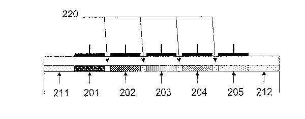
Figure 2 shows a cross section through the axial length of the waveguide of
the device. The EAM is split into sections 201, 202, 203, 204, 205, each
with a different bandgap and in which each bandgap section is addressed by
a separate electrode. The device may advantageously have low-loss
waveguides 211, 212 at its input and output. The different sections of the
device to which voltages are applied may advantageously be separated by
lengths of passive low-loss waveguide, 220.
Figure 3 shows a cross section through the device perpendicular to the
waveguide. The layer structure confines light in the vertical direction. Fig.
3 shows a ridge feature used to confine the light in the lateral direction,
but it
will be appreciated that other methods of providing confinement for the light
including buried heterostructures or antiresonant transverse waveguides
could be used.
6

CA 02479397 2004-09-15
WO 03/079100 PCT/GB03/01083
Figure 4 shows plan views of the device layout (with the contacts not shown
for clarity). Fig. 4(a) shows a device with a sequence of different bandgap
region formed sequentially along a single waveguide. Fig 4(b) shows two
parallel branches containing waveguide modulators. In this case, the light is
split into two parallel waveguides, each waveguide containing more than
one section of different bandgap. The light from each waveguide is then
recombined.
Other embodiments are intentionally within the scope of the accompanying
claims.
7

Representative Drawing
A single figure which represents the drawing illustrating the invention.
Administrative Status

2024-08-01:As part of the Next Generation Patents (NGP) transition, the Canadian Patents Database (CPD) now contains a more detailed Event History, which replicates the Event Log of our new back-office solution.

Please note that "Inactive:" events refers to events no longer in use in our new back-office solution.

For a clearer understanding of the status of the application/patent presented on this page, the site Disclaimer , as well as the definitions for Patent , Event History , Maintenance Fee  and Payment History  should be consulted.

Event History

Description Date
Time Limit for Reversal Expired 2010-03-15
Application Not Reinstated by Deadline 2010-03-15
Deemed Abandoned - Failure to Respond to Maintenance Fee Notice 2009-03-16
Letter Sent 2008-05-14
Request for Examination Received 2008-03-12
Request for Examination Requirements Determined Compliant 2008-03-12
All Requirements for Examination Determined Compliant 2008-03-12
Inactive: IPC from MCD 2006-03-12
Letter Sent 2005-06-14
Inactive: Single transfer 2005-05-16
Letter Sent 2005-01-12
Inactive: Single transfer 2004-11-24
Inactive: Cover page published 2004-11-24
Inactive: Courtesy letter - Evidence 2004-11-23
Inactive: Notice - National entry - No RFE 2004-11-16
Application Received - PCT 2004-10-18
National Entry Requirements Determined Compliant 2004-09-15
Application Published (Open to Public Inspection) 2003-09-25

Abandonment History

Abandonment Date Reason Reinstatement Date
2009-03-16

Maintenance Fee

The last payment was received on 2008-02-14

Note : If the full payment has not been received on or before the date indicated, a further fee may be required which may be one of the following

  • the reinstatement fee;
  • the late payment fee; or
  • additional fee to reverse deemed expiry.

Please refer to the CIPO Patent Fees web page to see all current fee amounts.

Fee History

Fee Type Anniversary Year Due Date Paid Date
Basic national fee - standard 2004-09-15
Registration of a document 2004-11-24
MF (application, 2nd anniv.) - standard 02 2005-03-14 2005-02-16
Registration of a document 2005-05-16
MF (application, 3rd anniv.) - standard 03 2006-03-14 2006-02-10
MF (application, 4th anniv.) - standard 04 2007-03-14 2007-02-16
MF (application, 5th anniv.) - standard 05 2008-03-14 2008-02-14
Request for examination - standard 2008-03-12
Owners on Record

Note: Records showing the ownership history in alphabetical order.

Current Owners on Record
INTENSE LIMITED
Past Owners on Record
JOHN HAIG MARSH
Past Owners that do not appear in the "Owners on Record" listing will appear in other documentation within the application.
Documents

To view selected files, please enter reCAPTCHA code :


To view images, click a link in the Document Description column. To download the documents, select one or more checkboxes in the first column and then click the "Download Selected in PDF format (Zip Archive)" or the "Download Selected as Single PDF" button.

List of published and non-published patent-specific documents on the CPD .

If you have any difficulty accessing content, you can call the Client Service Centre at 1-866-997-1936 or send them an e-mail at CIPO Client Service Centre.


Document
Description 
Date
(yyyy-mm-dd) 
Number of pages   Size of Image (KB) 
Drawings 2004-09-15 4 39
Claims 2004-09-15 3 83
Representative drawing 2004-09-15 1 9
Abstract 2004-09-15 1 58
Description 2004-09-15 7 266
Cover Page 2004-11-24 1 37
Reminder of maintenance fee due 2004-11-16 1 110
Notice of National Entry 2004-11-16 1 193
Courtesy - Certificate of registration (related document(s)) 2005-01-12 1 105
Courtesy - Certificate of registration (related document(s)) 2005-06-14 1 114
Reminder - Request for Examination 2007-11-15 1 119
Acknowledgement of Request for Examination 2008-05-14 1 190
Courtesy - Abandonment Letter (Maintenance Fee) 2009-05-11 1 172
PCT 2004-09-15 2 83
Correspondence 2004-11-16 1 27
Fees 2005-02-16 1 36
Fees 2006-02-10 1 35
Fees 2007-02-16 1 33