Note: Descriptions are shown in the official language in which they were submitted.
CA 02479622 2004-08-31
Supperrt ~i~ea~h~er 'With integrated t~r~ter~~aa Stt°neta~re
Meld ol° the Inventioa~
The invention relates to a anetlPod of producing an anteama structure for
as°~ autoanotive
vehicle, and to an antena~a structure for an automotive vehicle.
esca~ipti~n ot° the; Related ~r~t
in current automotive ea~.gia~eering, it ~s no longer possible to ianagine the
automotive
vehicle without antennae. In addition to the conventional audio appliances m
the form
of radios, modern automobiles furthermore have mobile-radio devices, Gl'S
systems,
television sets or further special partings, such as, for ~;xaa~ple;, a radio
central locking
system or the like. x.11 these fittings make a suitable antenna a~ecessary,
and tins
currently has the result that the numerous antennae or antenna systems in the
vehicle
are distributed at various points. In addition to conventional rod aerials, it
is known to
integrate antennae into the windscreen or rear window or to provide them at
other
points that ensure a good reception. The known car antennae systems are
subject,
however, to the disadvararage that, as a coalsequence of the distribution of
the antennae
at various points, the length ozcthe cable connectioa~as to the vehicle
distribution system
is l~aigh and tlae respective; cable harnesses are correspoa~adia~gly
comple~c. 1~urthermore,
2 0 manual fitting of the iaadividual antenna structures in v-ae vehicle is
very tnne-
consuming and, consequently, expensive.
correspondingly, the underlying object of the inveaztiors is to provide an
antenaia
structure for an automotive vehicle that permits an easy and rapid mounting in
tlae
~ 5 automotive vehicle together with an economical productioa~..
Summary e~f the Inventisan
The method of producing an antenna structure for an automotive vehicle in
accordance with the inve,atior=_ comprises the steps of providing a substrate
element,
3 0 and arranging said anteazaa;~, structure oat one surface of said substrate
element.
CA 02479622 2004-08-31
In an embodiment of the method according to the invention said antenna
structure is
applied by an etching method to o?ZC surface of said substrate element.
in an alternative embodiment of the method according to tl°~e
invention, said antenna
structure is applied to one surface of said substrate element by a
lithographic method,
by an evaporation method, by a sputtering method, by depositing a conductive
ink, or
by depositing a silver paste or the like.
In a further possible embodiment of the method according to the invention said
antenna structure has contact means which may be deposited on said surface of
the
substrate element as a delincd contact point.
according to a further possiblc embodiment of the method according to the
invention
the method comprises the, steps of mounting said substrate element on a
bodywork
component of the automotive vehicle by means of force-looked and/or shape-
locked
attachment means, the contact means of said antenna structure being connected
to a
distribution system of the automotive vehicle for the purpose of signal
transmission.
In a possible embodiment of the method according to the invention said
substrate
2 0 element is 'nounted on on.e side of the bodywork co~~nponent, which side
is opposite
an outside of the vehicle, v.Lhe bodywork component not being electrically
conductive.
1~urther, said bodywork co~npo~'ent may be a planar bodywork component, such
as, a
particular, a roof module, a boot lid or the like. Mill further., said contact
point of the
antenna structure may be ire contact connection with contact means formed
2 5 matchingly thereto on the bodywork corr~ponent in the case of said
substrate clement
being mounted.
The antenna structure ire accordance with the invention is disposed on a
substrate
element that is mounted as such on a bodywork component. any knov~m shape-
locked
30 and/or force-locked joints, for example in the form ofclip joints or plug
joints, gluing,
screwing and the like, are; suitable for mounting the substrate element. The
substrate
-z-
CA 02479622 2004-08-31
element may preferably be formed from a support sheet, which can be produced
particularly inexpensively.; for example in the form ol'a thermoplastic sheet.
The substantial advantage of tt~e antenna structure in accordance with the
invention is
that the antenna structure as such is already disposed in its entirety on
tl~Be substrate
element before the substrate element is mounted on a bodywork component. Since
the
possibly complex and ti:~~; -consuming steps of producing tlm antenna
structure on the
substrate element leave already been completed isa the preliminary stages of
the
mounting, fitting to the bodywork component itself can be performed in a very
time
saving way on the assembly line.
Yn an advantageous ret~ne~nenc of the invention, the antenna structure is
applied on the
surface of the substrate e:iement. The antenna structure, can be formed on the
surface
of the substrate elemeni using known methods for producing surface structures,
such
as, for example, an e~ra,poration and/or sputtering af~etllod in combination
with a
lithographic and/or an etching method. t1s an alternative to this, the antenna
structure
can also be formed by depositing conductive ink or :~llver paste or similar
conductive
materials on the surface c~f the substrate element. Further details on the
formation of
the antenna structure on the substrate element or on the surface of the
substrate
2 0 element are explained below.
In a further advantageous refinement of the invention, the antenna structure
comprises
contact means that are i~d contact connection 'vith corresponding contact
means on the
bodywork component for signal transmission so that -the antenna structure is
suitably
2 5 connected to the vehicle distribution system of the ac~torr~otive vehicle.
The mounting of the substrate element and making contact, necessary in this
connection, of the terminals of the an~:enna structure is advantageously
ensured by
defined contact points that are deposited on the surface of the substrate
element. The
30 bodywork component ~o which the substrate elerneru is attached has
correspondingly
contact means that are formed to match the defined contact points and that are
in
contact abutment with tlxe contact points of the antenna structure in the
mounted
-3~
CA 02479622 2004-08-31
substrate element. hrefcrably, the defined contact poinvs of the antenna
structure arc
formed on the surface of the substrate element as rein:forc~d Dads or the like
th~.t may
have a slightly raised contour =.vith respect to tlac sur~~ce of the substrate
cler-rae,nt for
fault-free signal trar°~srni,ssion so that they can relief>ly corm into
contact wi h the
contact means of the bod,yw~ork component.
In an advantageous re~ar~~ement of the invention? the support part is mounted
c,~n one
side of the bodyevo~°k corr~por~ent, which side is opposite to an
outside of the
automotive vehicle, the trodywork component not being electrically
conductive.. Such
a structure of the bodywc)rk part advantageously ensures that ~n undesirable
screening
of the antenna structure does not occur. In addition, such a fitting of the
substrate
element on the explained side of the bodywork coml>oncnt ensures that the
atatenna
structure is not darnaget~ by environmental factors or the like that prevail
on the
outside of the vehicle.
In an advantageous rcfr~emcnt of the inventions the hodywork component on
which
the substrate clement is mounted has a planar struciurc, in which connection,
said
bodywork component may preferably be a roof modtalc, a boot lid or the like.
Such
bodywork components ~~ffer a sufficiently large surt~:acc cvLn for complex
antenna
2 0 structures so that the various individual parts or additional parts of the
antenna
structure can be disposed next to one another on 9:1~e substrate element, and
this
advantageously results in a smaller oe~erall heigla. ls~ the abovementioned
roof
module, the boot lid or' tl~c like is r~adc of a plastic that is not
electrically condvgcting,
an excellent signal reccp~:ion is easily ensured for the a.ntcnna structure.
~~urther advantages and configurations ot''the inventia~n emerge from the
description
and the accompanying drawing.
It goes witho~.at saying that the abovemcntioned featur°c;s and those
still to be explained
below can be used not oily in the respective specificcz com'~inationg but also
in other
combinations or on tl'y~;ir own without departing zi-om the scope of the
present
invcntion°
CA 02479622 2004-08-31
~'he invention is schematically showr= in the drawings with reference to an
embodiment and is described in detail below with reference being made to the
drawing.
brief Description ~f the ~l~rawings
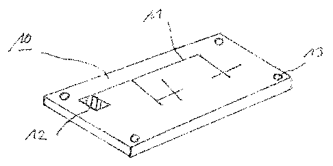
Fig. 1 shows a perspective view of a substrate element on which the antenna
structure in accordance with the invention is disposed.
Fig. 2 shows a cross-sectional side elevation of a substrate element with an
antenna structure integrated. therein in a state in which the substrate
element is mounted on a bodywork component.
Fig. 3 illustrates the performance of an evaporation process for producing the
antenna structure in accordance with the invention.
Fig. 4 illustrates the production of jhe antenna structure in accordance with
the
invention in accordance with the so-called "lift-off process".
2 0 Fig. 5 illustrates the production of the antenna structure in accordance
with the
invention in accordance with an etching method.
Detailed Description of vhc l<nvention
In a very simplified view, Fig. 1 shows, in perspective, a su'ostrate element
10 on
2 5 which an antenna structure 11 in accordance with the invention is
disposed. In detail,
the antenna structure is iraegrated in tlae, substrate element, i.e. it is
applied to a
surface of the substrate element. 'l'he substrate element 10 preferably
comprises a
support sheet, for exa~~ple a thern~oplastc sheet. Such a a;hermoplastic sheet
can be
back-formed or back-v~lleci with a furth~;r plastic on the side that is
opposite the
3 C antenna structure. Suitable for this purpose are back-forming with a PUIZ
system,
back-moulding with a thermoplastic material or, alternatively, back-embossing
with a
glass mat thermoplastic (~M'l~ or sheet-moulding-compound ~,SMC) material so
that
_5_
CA 02479622 2004-08-31
tl°~e support sheet can e~vdow sufficiently mcchanieal properties. As
an alternative to
this, that side of the scmbstrate, ~,lerrrent may also bc; back-formed or back-
filled to
which the antenna strc~ct~.~re is applied.
Diverse known ~.ethods of producing surface structures ~.re suitable for
applying the
antenna structure 11 to a sur face of the substrate element 10. A few of these
methods
are explained by way of example below.
In beneral, a conductor layer is applied, 'for example by means of the
evaporation or
sputtering method, to the surface of the substrate elek~aent 10. 'fo apply a
metal or a
conductive layer on the saarface of the substrate element, a known vacuum
reactor
comprising a suitable evaporation device is used as a rule, and this is shown
in a
simplified basic cross-se~.ti~~na1 elevation in Fig. ~.
An evaporation device ~0 in the form of the vacuum ~°eactor has a foell
jar 31 within
which a specimen, such as;, for eharrsple, the substrate element 10 is
disposed or is
horizontally suspended. From a side wall 32 of the bell jar ~l, a tube 33
branches off
outwards in which a pump device 3~ or tl~e like is installed. ~ reduced
pressure can
be produced inside the o~acuur~a reactor ~0 when the pump device 34 is
operated.
2 0 Furthermore, a so-called -5oat ~~ is disposed inside the bell jar 31 and
underneath the
point at which the substrate element 10 is disposed. ~f, for example,
alurniniurn is
applied to the substrate element 16I as the conductive layer, ~:he boat 35 is
provided
with an aluminium wire (not shown) that is evaporated by means of a heating
device,
an electron beam or the. lihe..
'the patterning of the conductive layer on the substrate element 10 is
preferably
achieved with the aid s~f ~a :jo-czlled "resist", i.e. polyn~~;r that is, as a
rule, radiation
sensitive. In the so-called ''lift-off process", the resist is applied to the
substrate
element 10 earlier in tigne than the conductive layer and the resist is
applied on the
3 0 conductive Layer already previously disposed on the suL>strate element in
the so-called
"etching method", the conductive layer there being subjected to an etching
process.
m6-
CA 02479622 2004-08-31
In the "lift-off process's, .he resist 41 (1~ig. Via) is first applied to the
surface of the
substrate element 10. suitable irradiation, for example L7~, ~-ray, ion or
electron
radiation, alters fhe properties of the resist 41 in a controlled way at the
exposed
points. This makes possible a selective removal of tl~e irradiated (positive
method) or
of the unirradlated regions (tlegative n~cethod~,. S~aitablc for producing the
desired
antenna structure is, fc~r example, ~~I lithography, with which structures in
the
micrometer range can readily be obtained. ~ working rnaslc through which the
resist
41 is exposed is, as a rule., used in this type of lithography. .~s an
alternative to this,
the exposure of the res3s~; loss also be performed by means of so-called
electron beam
0 lithography. In this techniciue, an electron beam is used to pattern the
resis~~ Layer. An
advantage of this method is, in addition to the high resolution, th.e great
flexibility of
this patterning method since, for example, in contrast to 1.J~ lithography, no
masks are
needed since any desired structures can be produced as a e~AL~ file or
directly on the
resist to be irradiated by means oI°suita6le control software.
t~s a result of the lithc~gr~,phy, some regions of the resist 41 are
selectively removed.
The remaining layer of tope resist 41 consequently has xhe function of
protecting the
material of the substrate c lerrlent 10 underneath it agairdst file effects of
the subsequent
application of a conducti~;re layer. Expressed in other ~n~crds, only those
regions of the
2 0 substrate element 10 at v~hich parts of the resist have been ren~loved are
coated with a
conductive layer in the evaporation method already explained above. Figs 4a to
4c
show the sequence of ?hese steps in tile method according to the lift-off
process in a
simplified basic sketch.
2 5 Fig. 4a shows a cross-sectional side elevation of the substrate element 10
to whose
surface l0a the radiation-sensitive resist 41 is applied. Irl the diagram of
Via, the resist
41 has already been subjected to lithography, as explained above, with the
result that,
for example, a central region of the resist has been re~loved and,
consequently, the
underlying surface 10a of the; substrate element 10 has been exposed.
In a subsequent step, the substrate element is subjected to arl e~~aporation
method (cf.
explanation of Fig. ~), as a result of~vhich one surface l0a o.f the substrate
element 10
CA 02479622 2004-08-31
is coated with a conductive layer 42. As shown in Fig. 4b, the conductive
layer 42 is
applied in the same way to the ~-ernaining regions of the resist 41 as also to
the
exposed part of the surface 10a of the sc~bstrate element l0. Subsequent
thereto, as
shown in Fig. 4c, the remaining part of the resist 41 and together therewith
the
conductive layer 42 disposed thereon is removed in a suitable way. !-~,s a
result, there
remains behind on the surface l0a ofthe substrate elernPnt 10 a part of the
conductive
layer 42 that forms the antenna structure 11 as desired. 1n the case of tl~e
positive
method, precisely those regiorgs of the resist that c~orrespo~d to the later
antenna
structure 1 i on the substrate element l (> have already been irradiated arid.
thereby
1C? selectively removed dur~:~g the irradiation of the resist by means of the
abovementioned lithography.
A,s an alternative, the antcrana structure can also be sr~itably produced by
the etching
method. In that case, the surface 10a of the su~~strate ele~~ent l U is first
completely
coated with a suitable conductive layer 42 or a metal. 'f he substrate element
10 is
shown in such a state in a simplified cross-sectional side elevation in Fig.
Sa.
In a subsequent step in the method, as explained above, the irradiation-
sensitive resist
41 is applied to the surface 1Ua or on the conductive layer 42 in the sane way
and
2 0 selectively removed by means of a suitable lithographic method so that the
conductive
layer 42. is exposed to the outside at these points. This state of the
substrate element
10 is shown in Fig. Sb. S'ubsequent thereto, in accordance with the diagram of
Fig. Sc,
are etching method is performed, with the result that the conductive layer 42
is
substantially completely removed in those regions in which it is not covo:,red
by the
resist 41. A dry etching method with which a l~kigh anisotropy and,
conseduet~tly very
sharp structures can be produced in the mask region is preferably suitable for
performing the etching method. In detail, the dry etch.ang method can be
performed by
a knoe~~n chemical etcl~in;~ or a known physic~~l etching. ~s an alternative
to this, a
known wet-chemical method is in principle also possible for etching the
conducting
3 0 layer 42.
_$_
CA 02479622 2004-08-31
In a final step in the znc;thod, those regions of the ra.sist ~-1 that are
formed on the
conducting layer 42 are removed i:*z conjunction with the etching method. ~s a
result,
only isolated regions of the conducting layer 4~ that ultirrzately form the
desired
antenna structure 11 consequently remain behind on the surface 10a of the
substrate
element.
~s a departua-e from tl~ze :;t~;ps in the method explained. ~.vith reference
to ~~igs 3 and ~,
the antenna structure can be deposited in the earns way or the surface ~ Oa of
the
substrate element 10 in Hlzs~ form of a conducti~~e ink. In view of the high
precision
always required and sirz~ulE:aneously favourable prodm;,tio$z costs, a
dispensing device
can in this case be used that is preferably guided, for ~;xaz~ple, by means of
a robot or
the like and from which ~ t~; conductive ink is dispensed. Instead of a
conductive ink, a
silver paste or a similar conductive material can be a<.ced in the same way,
as a result
of which the antenna structure 11 is provided on the surface 10a of the
substrate
element 10.
The antenna st~-uctur~; 11 furtlZermore comprises contact means in the fore.
of a
contact pad 12 that is likewise applied to the surface e'f the substrate
element 10. The
contact pad l~ serves to suitably connect the antenna structurre 11 to a
vehicle
2 0 distribution system of an autorr~otive vehicle in order to ensure signal
transmission to
various terminal appliancecj such as a radio, television set, ~hS system,
mobile-radio
system or the like.
To mount the substrate ele~~~en,: 10 on a bodywork cors°~ponent, a
plurality of through
2 5 bor°es 13, for example, may be provided in each of the corners of
the substrate element
10 with which the substrate element 10 can be suitably screwed to the bodywork
component. 1-Ioweve,r, other v~~ays of mounting the ,substrate element 1.0 on
the
bodywork components az°e equally possible. Thus, the substrate element
10 may also
be attached to the bodywork cornzponent by gluing, clipping or the like.
~'ig. ~ shows the substrate element 10 with the antenna strr~cture 11
integrated therein
in a state in which it is mounted on a bodywork component 14. T his fig.
illustrates
-9-
CA 02479622 2004-08-31
only the principle of~nou~nting the substrate element and is accordingly a
ccsnsiderably
simplified diagram. ~ he substrate element 10 substantially flushly abuts one
side 15
of the bodyvaork co~npor~ent 14, 'vhich side 15 is opposute an outside 16 of
the
vehicle. if the body~srorl~~ s;omponent is, ~'or example, ~ roof module made
of plastic,
the substrate element 10 is co9-respondingly attached '~o an inside of the
roof module
so that the substrate element 1 C~ is not exposed to environmental factors and
the like.
~'o attach the substrate element 10 to the bodywork c~rrnponent 14, snap hooks
16, for
example, may be ~~ved to the bodyevork component. ~ he snap hooks 16
advantageously engage around a respective ri~n of the substrate element 10 so
that,
after being pressed against the side 15 of the body°c?rk component 1~,
the substrate
element 10 can suitably latch in position by means o:l° the snap hooks
16. In addition
or alternatively, the substrate elegnent 10 cnay be acre«red to the bodywork
component
14 by means of throughbor es 13. bluing the substrate clement 10 to the side
15 of the
bodywork component 1 ~ with suitable and preferably rapidly curing adhesives
is
equally possible.
The bodywork component 1~ has contact means 2~, that are farmed on the side
15, for
example, in flee forge o~ a conductive co~~tact. ~,he contact 22 is connected.
by means
2 0 of an electrical line ~~ to a cable harness or to the vcrhicl~;
distribution system of the
automotive vehicle. the substrate element 20 &s suitably Fnounted on the side
15 of
the bodywork component 14 in such a svay that the contaca pad 12 of tl:ae
antenna
structure i l abuts the cfantact 2~. In this state shown in 1~'ig. 2, an
interfcrrence-free
contact is ensured o~ the antenna structure 11 with the distribution network
of the
2 5 automotive vehicle via the contact pad 12, with the result that an
excellent signal
transmission is ensured. 1:o the respective terminal appliances in the
automotive
vehicle, for example a radio, Ci~~ system, a tr~obile--radio system, radio
device for
central locking and the 1~3c~;.
- 10-