Note: Descriptions are shown in the official language in which they were submitted.
CA 02479683 2012-02-16
SEMICONDUCTOR-NANOCRYSTAL/CONJUGATED POLYMER
THIN FILMS
STATEMENT AS TO RIGHTS TO INVENTIONS MADE UNDER
FEDERALLY SPONSORED RESEARCH OR DEVELOPMENT
The invention described and claimed herein was made in part utilizing funds
supplied by the United States Department of Energy under contract NO. DE-AC03-
76SF000-
98 between the United States Department of Energy and The Regents of the
University of
California. The government has certain rights to the invention.
BACKGROUND OF THE INVENTION
The first solar cells were fabricated in the mid 1950s from crystalline
silicon wafers.
At that time, the most efficient devices converted 6% of solar power to
electricity.
Advancements in solar cell technology over the past 50 years have resulted in
the most
efficient Si cell at 25% and commercial Si modules, an array of cells, at 10%.
Although Si,
in crystalline and polycrystalline forms, is the most common type of material
used in solar
cells, other semiconductors such as gallium arsenide, indium phosphide and
cadmium
telluride are being investigated for the next generation of higher efficiency
solar cells. In
particular, high efficiency structures such as tandem cells, in which multiple
band gaps are
1
CA 02479683 2004-09-17
WO 03/081683
PCT/US03/08624
layered in a single device. using Ga1nP, GaAs and Ge have attained record
efficiencies of
34%.
Despite these impressive efficiencies, the high cost of manufacturing solar
cells of
the prior art limits their widespread use as a source of power. The
construction of prior art
commercial silicon solar cells involves four main processes: the growth of the
semiconductor
material, separation into wafers, formation of the device and its junctions,
and encapsulation.
For the cell fabrication alone, thirteen steps are required to make the solar
cell and of these
thirteen steps, five require high temperatures (300 C-1000 C), high vacuum or
both. In
addition, the growth of the semiconductor from a melt is at temperatures above
1400 C under
an inert argon atmosphere. To obtain high efficiency devices (>10%),
structures involving
concentrator systems to focus sunlight on to the device, multiple
semiconductors and
quantum wells to absorb more light, or higher performance semiconductors such
as GaAs and
InP, are needed. The gain in performance results in increased manufacturing
costs, which
stem from the multiplication of the number of fabrication steps. To date,
these high
performance architectures have been employed mainly for extra-terrestrial
applications such
as in space shuttles and satellites, where efficiency per unit weight is as
important as
fabrication costs.
Another problem with the solar devices of the prior art is the high cost of
manufacturing materials. The amount of silicon needed for lkW of module output
power is
approximately 20kg. At $20/kg, the material costs for electronic grade silicon
is partially
subsidized by the chip manufacturing sector. Other materials such as GaAs,
which are
synthesized with highly toxic gases, are a factor of 20 higher in cost at
$400/kg. Because
solar cells are large area devices, such material costs hinder the production
of inexpensive
cells. As a result, thin film devices, which have active layers several
microns thick of
amorphous Si, CdTe, and CuInSe2 are being explored. In 1991, O'Regan et al.
reported the
invention of a novel photochemical solar cell comprised of inexpensive TiO2
nanocrystals
and organic dye, O'Regan et al. Nature 353, 737 (1991).
Bilayer devices, from spin casting a derivative of polythiophene on which a
layer of
Cal is evaporated, have been able to reach a maximum external quantum
efficiency (EQE) of
23%. Higher efficiencies at 50% were obtained from blending derivatives of Co
and MEH-
PPV into a homogeneous film for a single-layer device. Further improvements in
efficiencies
are limited by the poor electron transport properties of C60, which is
characterized by
hopping, and the low overlap between the device absorption and the solar
emission spectrum,
Greenham. N.C. et al., Phys Rev. B, Vol. 54, No. 24, Dec 1996.
2
CA 02479683 2013-01-25
It has been suggested previously to use CdSe particles in poly(3-
hexylthiophene), see
Alivisatos et al. Adv. Mater_ 1999, 11, Na 11. This work only teaches the use
of
nanocrystals less than 13 nm in size and the devices produced do not approach
the
efficiencies of those of the instant invention. Further, this prior art admits
solution chemistry
problems with nanorods and offers no solutions to the problems solved by the
invention
described herein. Solar cells based on inorganic nanorods according to the
instant invention,
which have good transport properties and absorption spectra that can also be
extended into
the near infrared, can potentially reach efficiencies that rival conventional
solar cells based on
bulk inorganic semiconductors. It is the thin films incorporating
semiconductor-nanocrystals
according to the embodiments of this invention that provide solutions to the
above stated
problems.
SUMMARY OF THE INVENTION
The invention described herein provides for thin films and methods of making
comprising inorganic semiconductor-nanocrystals dispersed in semiconducting-
polymers in
high loading amounts. The invention also describes photovoltaic devices
incorporating the
thin films.
According to an embodiment of the present invention, there is provided a thin
film for
use in a photovoltaic device, the thin film comprising: a semiconducting
conjugated
polymer having at least 5 wt % semiconductor-nanocrystals embedded therein,
wherein:
at least a portion of the semiconductor-nanocrystals have an aspect ratio
greater than
about 2, and wherein the thin film is capable of providing a power conversion
efficiency
greater than 2% at A.M. 1.5 global illumination when in the photovoltaic
device.
According to another embodiment of the present invention, there is provided a
photovoltaic device, comprising: the thin film as described herein.
BRIEF DESCRIPTION OF THE DRAWINGS
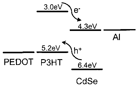
FIG I shows an energy level diagram for CdSe and P3HT which shows a schematic
of process of charge transfer between 5nm CdSe and P311T..
FIG 2 shows a schematic of the structure of a nanorod-polymer blend
photovoltaic
device according to one embodiment of the invention.
FIG 3 shows a low resolution 71-Ervl image of a) 7 nut by 7 nm, b) 8 rn by 13
nm, c)
3 TIM by 60 nm, and d) 7 nm by 60 nm CdSe nanocrystals
3
CA 02479683 2013-01-25
FIG 4 shows a AFM¨TM topography image of a film consisting of 90 wt. % 7 nm by
7 nm CdSe nanocrystals dispersed in P3HT, spin cast from chloroform. The scan
area is 5
FIG 5 shows a AFM-TM a) topography and b) phase images of films consisting of
90
wt. % 9 nm by 13 nm CdSe nanocrystals dispersed in P3HT spin cast from 1 vol.
% and 8
vol. % pyridine in chloroform. Images are presented at the same scale for a
scan area of 5
15
3a
CA 02479683 2004-09-17
WO 03/081683
PCT/US03/08624
FIG 6 shows surface roughness (open circles) of films consisting of 90 wt. % 9
nu] by
13 nm CdSe nanocrystals dispersed in P3HT spin cast from various
concentrations of
pyridine in chloroform. The maximum EQE (solid diamonds) is shown of devices
made from
these films. Lines serve as a guide to the eye.
FIG 7a shows a normalized photocurrent spectra for a 90 wt. % 3 nm by 60 nm
CdSe
nanorods in P3HT device (open circles) and after annealing at 120 C (solid
squares).
FIG 7b shows the ratio of the EQE before and after heat treatment as a
function of
wavelength for 90 wt. % 3 nm by 60 nm CdSe nanorods in P3HT device and a
nanorod-only
device. The inset shows the individual 1-transmission spectra for 3 nm by 60
nm CdSe and
P3HT.
FIG 8 shows the relative contribution of P3HT to the absorption (solid
diamond,
dashed line), photocurrent (open circle, solid line) and photocurrent after
120 C heat
treatment (solid square, dashed line) of series of 3 nm by 60 nm nanorod
devices in P3HT at
various nanorod concentrations.
FIG 9 shows the EQE of 90 wt. % 7 nm by 14 nm CdSe in P3HT under ¨ 0.1
mW/cm2 illumination at 515 nm. The inset shows the PL efficiency of 60 wt. % 7
nm by 14
nm CdSe in P3HT samples under 514 nm excitation after heat treatment at
various
temperatures.
FIG 10 shows the EQE spectra of a 90 wt. % 7 nm by 60 nm CdSe nanorods in P3HT
(open circles) and after 120 C heat treatment (solid squares). Inset: the
corresponding
current-voltage characteristics, under illumination of 0.1 mW/cm2 at 515 nm,
for this device,
which includes an open circuit voltage of 0.4 V and a fill factor of 0.5.
FIG lla shows the EQE spectra of devices from 90 wt. % 7 nm by 60 nm CdSe
nanorods in P3HT with thickness 212 nm, 271 nm and 346 nm before 120 C heat
treatment.
FIG llb shows the EQE spectra of devices from 90 wt. % 7 nm by 60 nm CdSe
nanorods in P3HT with thickness 212 nm, 271 nm and 346 nm after 120 C heat
treatment.
FIG 12a shows the relative enhancement of the EQE before and after heating at
120
C for devices in FIG lla and 11b.
FIG 12b shows the absolute difference in EQE before and after heat treatment.
FIG 13a shows a TEM of a thin film of 20 wt. % 3nm by 60nm CdSe nanorods and
P3HT spin cast from chloroform.
FIG 13b shows a TEM of the same nanocrystals of FIG 13a when cast from a 10
vol.% pyridine in chloroform solution.
4
CA 02479683 2004-09-17
WO 03/081683
PCT/US03/08624
FIG 14 shows a TEM of a cross section of a 100 nm film consisting of 60 wt. %
lOnm
by lOnm CdSe nanocrystals in P3HT
FIG 15a shows a 7nm by 60nm CdSe nanorods.
FIG 15b shows a TEM of a cross section of a 100nm film consisting of 40 wt. %
CdSe nanorods in P3HT.
FIG 16 shows as the length of a 7nm diameter nanorod is increased successively
from
7nm to 30nm and to 60nm, the EQE for the 90 wt. % CdSe in P3HT devices, rises
by almost
a factor of 3 to 54%, under illumination of 0.084mW/cm2 at 5I5nm.
FIG 17a-c shows a TEM of 7 nm diameter nanocrystals with lengths, a) 7nm, b)
30nm
and c) 60nm. The scale bar is 50nm and all TEMs are at the same scale.
FIG 18 shows a the EQE for the 90 wt. % 3nm by 100nm branched CdSe nanorods in
P3HT devices as a function of pyridine concentration.
FIG 19a shows tetrapod nanocrystals unaligned.
FIG 19b shows tetrapod nanocrystals alligned.
FIG 20 shows the EQE spectra for a series of 90 wt. % 7 nm by 60 nm CdSe in
P3HT
devices with different film thicknesses.
FIG 21a shows the EQE spectra for 90 wt. % 7 nm by 7 nm CdSe in P3HT at
various
film thicknesses.
FIG 21b shows the corresponding absorption spectra for these devices, shown as
a
function of increasing thickness.
FIG 22a shows a TEM of 40 wt% 5 nm CdSe nanocrystals in P3HT for TOPO treated
nanocrystals.
FIG 22b shows a l'EM of 40 wt% 5 nm CdSe nanocrystals in P3HT for T1 treated
nanocrystals.
FIG 24 shows a TEM of 40 wt% 5 nm CdSe nanocrystals in P3HT for pyridine
treated nanocrystals.
FIG 23a shows the I-V characteristics for 90 wt. % 7 nm by 60 nm CdSe nanorods
in
P3HT under 0.1mW/cm2 illumination at 515nm.
FIG 23b shows the solar cell characteristics of the same FIG 23a device,
measured
with a simulated AM 1.5 Global light source, include a short-circuit current
of 5.7mA/cm2, a
FF of 0.42, and an open-circuit voltage of 0.67V to yield a solar power
conversion efficiency
of 1.7%.
FIG 24 shows both the ideal and a typical I-V curve found experimentally.
5
CA 02479683 2004-09-17
WO 03/081683
PCT/US03/08624
DETAII FD DESCRIVIION OF THE PREFERRED EMBODIMENTS
In one embodiment of the invention there is disclosed a thin film comprising
a semiconducting conjugated polymer having at least 5 wt% semiconductor-
nanocrystals
embedded therein.
In another embodiment there is disclosed a photovoltaic device comprising the
thin
film of this invention.
In another embodiment of this invention there is disclosed a process of making
a
polymeric thin film comprising washing surfactant coated semiconductor-
nanocrystals with a
solvent at least one time, and codissolving the washed semiconductor-
nanocrystals and a
semiconducting polymer in a binary solvent mixture, and depositing the
mixture.
In another embodiment of the invention there is disclosed process of making a
photoactive thin film comprising dispersing semiconductor-nanocrystals having
an aspect
ratio of greater than 2 in a semiconducting conjugated polymer to provide a
polymer-
nanocrystal composite, and depositing a thin film of said composite, such that
the
nanocrystals are embedded in the polymer at greater than 5 wt%.
In another embodiment of the invention there is disclosed a photovoltaic
device,
comprising a conjugated conductive polymeric layer having semiconductor-
nanocrystals
dispersed therein where the device has an power conversion efficiency greater
than 1% at
AM 1.5 global illumination.
In another embodiment of the invention there is disclosed a photovoltaic
device
comprising a first planar electrode, a thin film comprising a semiconducting
conjugated
polymer having semiconductor-nanocrystals ernbedded therein, the thin film
being deposited
on the first planar electrode, and a second electrode opposite the first
electrode, and a hole
injecting layer disposed between the thin film polymeric layer and the first
planar electrode.
In preferred embodiments of this invention the semiconductor-nanocrystals will
have
an aspect ratio of greater than 2, preferably greater than 5, more preferably
between about 5
and 50. Most preferred is about 10.
In preferred embodiments of this invention there is disclosed the dispersion
or
embedding of semiconductor-nanocrystals in the semiconducting-polymer.
Preferably this
"loading" is on the amount of greater than 5 wt%. More preferably, this amount
is between
20 and about 95 wt%. Even more preferably the amount is between 50 and about
95 wt%.
Most preferably the amount is about 90 wt%.
6
CA 02479683 2004-09-17
WO 03/081683
PCT/US03/08624
In preferred embodiments of this invention the semiconducting polymer will be
a
polymer or blend chosen from trans-polyacetylenes, polypyrroles,
polythiophenes,
polyanilines, poly(p-phenylene)s and poly(p-phenylene-vinylene)s,
polyfluorenes,
polyaromatic amines, poly(thienylene-vinylene)s and soluble derivatives
thereof. Preferred
are (poly(2-methoxy5-(2'-ethylhexyloxy)p-phenylenevinylene) (MEH-PPV) and
poly(3-
hexylthiophene, (P3HT), with P3HT being the most preferred.
In preferred embodiments, the semiconductor-nanocrystals comprise rods having
lengths greater than about 20 nm. More preferred are rods having a length of
between 20 and
200 nm. Even more preferred are rods having lengths of between about 60 and
110 nm.
In more preferred embodiments the invention discloses the use of Group
Group
III-V, Group IV semiconductors and tertiary chalcopyrites. More preferred are
CdSe, CdTe,
InP, GaAs, CuInS2, CuInSe2, AlGaAs, InGaAs, Ge and Si, and even more preferred
is CdSe.
It is preferred that the semiconductor nanocrystals be branched nanocrystals.
More
preferred nanocrystals having 4 arms and tetrahedral symmetry.
It is preferred that the thin film of this invention have a thickness of about
200nm.
It is preferred that the process for making the thin film of this invention
use a binary
solvent mixture where at least one of the solvents is chosen from the group
consisting
pyridine, chloroform, tolulene, xylenes, hexanes, water, dichlorobenzene,
methylene chloride,
an alkylamine, where the alkyl chain may be branched or unbranched and is
between 2 and
20 carbons in length, butanol, methanol and isopropanol. Most preferred is
pyridine in
chloroform.
It is preferred that the binary solvent mixture be in an amount of between 1-
15 vol%,
with a more preferred range being 4-12 vol %, and most preferred is 8 vol%.
In another embodiment of the invention described herein there is disclosed a
method
for making polymeric thin films having incorporated therein semiconductor
nanocrystals
where there is a step of washing the surfactant coated semiconductor
nanocrystals at least
once with a solvent, preferred in pyridine.
In another embodiment of the invention described herein is a method for making
a
polymeric thin film comprising thermal annealing of the deposited film at a
temperature of
from 60 C to about 200 C. Preferred is about 120 C.
In another embodiment of the invention there is disclosed herein a
photovoltaic device
incorporating a PEDOT:PSS (poly(ethylene-dioxy)thiophene:poly(styrene
sulphonic acid))
hole transporting layer on top of an ITO electrode.
7
CA 02479683 2004-09-17
WO 03/081683
PCT/US03/08624
By "semiconductor-nanocrystal" it is meant to include semiconducting
crystalline
particles of all shapes and sizes. Preferably, they have at least one
dimension less than about
- 100 nanometers, but they are not so limited. Rods may be of any length.
"Nanocrystal",
"nanorod" and "nanoparticle" can and are used interchangeably herein. In some
embodiments
of the invention, the nanocrystal particles may have two or more dimensions
that are less than
about 100 nanometers. The nanocrystals may be core/shell type or core type.
For example,
some branched nanocrystal particles according to some embodiments of the
invention can
have arms that have aspect ratios greater than about 1. In other embodiments,
the arms can
have aspect ratios greater than about 5, and in some cases, greater than about
10, etc. The
widths of the arms may be less than about 200, 100, and even 50 nanometers in
some
embodiments. For instance, in an exemplary tetrapod with a core and four arms,
the core can
have a diameter from about 3 to about 4 nanometers, and each arm can have a
length of from
about 4 to about 50, 100, 200, 500, and even greater than about 1000
nanometers. Of course,
the tetrapods and other nanocrystal particles described herein can have other
suitable
dimensions. In embodiments of the invention, the nanocrystal particles may be
single
crystalline or polycrystalline in nature. The invention also contemplates
using nanorods of
CdSe and CdTe that have have aspect ratios above 20, even up to 50, and
lengths greater than
100 nm, formed according to processes described in the literature, see Peng,
X.G. et al.
Nature 404, 59 (2000) and Peng, Z.A. et al. J. Am. Chem Soc. 123, 183 (2001).
The length of semiconductor-nanocrystal rods used herein have lengths between
20
and 200 nm. In preferred embodiments, the semiconductor-nanocrystals comprise
rods
having lengths greater than about 20 nm. More preferred are rods having a
length of between
20 and 200 nm. Even more preferred are rods having lengths of between about 60
and 110
nm.
By "at least a portion of the semiconductor-nanocrystals have an aspect ratio
greater
than about 2" it is meant that if the semiconductor-nanocrystals are
unbranched rods, then at
least part of the total amount of the rods will have an aspect ratio of
greater than about 2. The
amount could be as high as 100%. Also, this means that if the nanocrystals are
branched
semiconductor-nanocrystals (which of course includes tetrapods), then "at
least a portion"
means that at least one branch has an aspect ratio of greater than 2. Aspect
ratio is defined as
the length of the longest dimension of a rod divided by its diameter. In the
case of a branched
nanocrystal, the aspect ratio for the branched nanocrystal is defined as the
length of the
longest branch divided by the longest branches diameter.
8
CA 02479683 2012-02-16
By "a portion of the semiconductor-nanocrystals are branched nanocrystals" it
is
meant that at least 1% by weight of the nanocrystals are branched
nanocrystals. It is
understood that the language "a portion" as defined herein could also include
100%0, i.e. the
"whole portion".
Although CdSe and CdTe semiconductor- nanocrystals are preferred, the
nanocrystal particles may comprise other suitable semiconductor material, and
be a rod, a
shaped particle or a sphere. For example, the particles may comprise
semiconductors such as
compound semiconductors. Suitable compound semiconductors include Group II-VI
semiconducting compounds such as MgS, MgSe, MgTe, CaS, CaSe, CaTe, STS, SrSe,
SrTe,
B aS, BaSe, BaTe, ZnS, ZnSe, ZnTe, CdS, CdSe, CdTe, HgS, HgSe, and HgTe. Other
suitable compound semiconductors include Group IH-V semiconductors such as
GaAs, GaP,
GaAs-P, GaSb, InAs, InP, InSb, AlAs, A1P, AlGaAs, InGaAs and AlSb. The use of
Group
IV semiconductors such as germanium or silicon may also be feasible under
certain
conditions. In other embodiments, the particles may comprise a dielectric
material such as
SiC, SiN Of any other material that can exhibit polytypism. Also included are
the tertiary
chalcopyrites, for example CuInS2 and CuInSe2. Some metals such as Fe, Ni, Cu,
Ag, Au, Pd,
Pt, Co and others may also exhibit polytypism and can be used in embodiments
Rod, Arrow,
Teardrop and tetrapod shaped semiconductor nanocrystals are defined in Manna
et al. J. Am.
Chem Soc. 2000, 12, 12700,12706,
The nanocrystal particles according to embodiments of the invention can have
unique
optical, electrical, magnetic, catalytic, and mechanical properties, and can
be used in a
number of suitable end applications. They can be used, for example, as fillers
in composite
materials, as catalysts, as functional elements in optical devices, as
functional elements in
photovoltaic devices (e.g., solar cells), as functional elements in electrical
devices, etc.
By "P3HT" it is meant poly(3-hexylthiophene), which includes regioregular
P3HT,
which includes head to head and also head to tail regioregular P3HT. Preferred
is head to tail
P3HT.
This invention contemplates that any semiconducting conjugated polymers that
can be
processed from solution will function in accordance with this invention. By"
semiconducting
polymer" it is meant all polymers that have a pi-electron system. Non-limiting
examples
include trans-polyacetylene, polypyrrole, polythiophene, polyaniline, poly(p-
phenylene and
poly(p-phenylene-vinylene), polyfluorenes, polyaromatic amines,
poly(thienylene-vinylene)s
and soluble derivatives of the above. An example is (poly(2-rnethoxy,5-(2'-
ethylhexYloxY)1)-
9
CA 02479683 2004-09-17
WO 03/081683
PCT/US03/08624
phenylenevinylene) (MEH-PPV) and poly(3-alkylthiophene). Especially preferrred
is
poly(3-hexylthiophene), P3HT. This invention also contemplates using
conjugated polymers
that are either solution processable or melt processable because of bulk
pendant groups
attached to the main conjugated chain or by its inclusion of the conjugated
polymer into a
copolymer structure of which one or more components are non-conjugated. Non-
limiting
examples include poly(,4'-diphenylenediphenylvinylene), poly(1,4-phenylene-l-
phenylvinylene and poly(1,4-phenylenediphenylvinylene, poly(3-alkylpyrrole)
and poly(2,5-
dialkoxy-p-phenylenevinylene). It is understood that by semiconducting
conjugated polymer
this could mean a mixture of blend of polymers, one of which is to be a
semiconducting
conjugated polymer. Thus the nanocrystals are or would be embedded or
dispersed in the
blend or mixture.
This invention further contemplates that the semiconducor-nanocrystals, rods,
can be
aligned by any techniques known in the art for aligning crystals.
By "photovoltaic device" it is meant to include those typical device
architectures
known in the art. Exemplary photovoltaic devices are described in, for
example, Science,
Vol. 295, pp. 2425-2427, March 29, 2002, the contents of which are
incorporated by
reference. An exemplary photovoltaic device may have nanocrystal particles in
a binder.
This combination can then be sandwiched between two electrodes (e.g., an
aluminum
electrode and an indium tin oxide electrode) on a substrate to form a
photovoltaic device.
By "binary solvent system" it is meant to include a system of two solvents,
and one
may be a ligand that is also a solvent. For example, pyridine in chloroform.
"Binary solvent
system" is also meant to include a system of at least one solvent, and a
ligand that is not a
solvent, for example xylene and phosphonic acid. Xylene is a solvent for the
semiconductor
nanocrystal and phosphonic acid is a ligand, but not a solvent.
Suitable methods for making thin films like those described herein are known.
Non-
limiting examples of various coating and printing techniques from solution
include spin
coating, blade coating, dip coating, inkjet printing and screen printing. All
of these
techniques are generally referred to herein as "depositing". That is, the thin
films of the
instant invention have to be "deposited" onto a substrate of some form.
The complementary electronic properties of inorganic and organic
semiconductors
can be used in the formation of electrically active junctions. Charge transfer
is favored
between high electron affinity inorganic semiconductors and relatively low
ionization
potential organic molecules and polymers. In one embodiment of the instant
invention
semiconductor nanoparticles, such as CdSe nanocrystals are combined with
conjugated
CA 02479683 2004-09-17
WO 03/081683
PCT/US03/08624
polymers such as P3HT to create charge transfer junctions with high
interfacial area resulting
in photovoltaic devices having improved efficiency. From the energy level
diagrams for
CdSe nanocrystals and P3HT, it can be seen that CdSe is electron-accepting and
P3HT is
hole-accepting (FIG 1). The presence of ligands on the surface of nanocrystals
mediates its
interaction with the polymer. We can replace or remove ligands on the surface
of CdSe
through chemical washing of nanocrystals or heat treatment of CdSe-P3HT blend
films after
they have been cast.
The effectiveness of charge transfer and transport is determined by the
morphology
of the blend. Aggregation of nanocrystals both in solution and in the polymer
depends on the
strength of the van der Waals interaction between the particles and thus on
the separation
between nanocrystals and their size. A balance between aggregation for
transport of electrons
and dispersion for more efficient charge transfer is required. The inventors
have surprisingly
discovered that fine control of morphology is obtained through the use of
solvent mixtures.
Solvent mixtures according to embodiments of this invention that contain
pyridine, which is a
ligand and solubilizes nanocrystals, can influence the dispersion of the
nanocrystals in
solution. Since spin casting is a non-equilibrium process, the dispersion of
the nanocrystal in
solution can be maintained in the polymer.
According to one embodiment of the invention a solvent mixture is used to
control the
phase separation down to the nanometer scale. The inventors have surprisingly
found that it is
possible using a solvent mixture to control phase separation in a film with a
high
concentration of nanocrystals (up to 90-95 weight %) in polymer, in particular
P3HT down to
the nanometer scale. The aim is to enhance the solubility of the nanocrystals
by
simultaneously using a good solvent and ligand for nanocrystals, and in
particular CdSe, and
a good solvent for the polymer for solution processing. A preferred example is
the weak-
binding Lewis base, pyridine, with its relatively low boiling point of 116 C
which was chosen
as a ligand for the nanocrystals with the aim of facile removal. Pyridine
treated nanocrystals
of various shapes and sizes (FIG 3) were co-dissolved with P3HT in a mixture
of 4% to 12%
by volume (vol. %) pyridine in chloroform to create a uniform film consisting
of dispersed
particles in polymer when spin cast. The preferred amount of pyridine to cover
the
nanocrystal surface is determined by the number of non-passivated Cd surface
sites on the
nanoparticle. Pyridine is miscible in chloroform, so that there is a twofold
solubility increase
for the nanocrystals: (a) pyridine coated nanocrystals are more soluble in
chloroform than
their naked counterparts and (b) they are highly soluble in the excess
pyridine that is not
bound to nanocrystals. Too much pyridine, however, is to be avoided, as this
mediates the
11
CA 02479683 2004-09-17
WO 03/081683
PCT/US03/08624
precipitation of P3HT, which is very soluble in chloroform and insoluble in
pyridine.
Therefore, there are three solubility regimes:
1. The low pyridine concentration regime: Insufficient solubility of
the nanocrystals
results in large-scale phase separation in the blend films promoted by
nanocrystal
flocculation.
II. The intermediate pyridine concentration regime: Provided that the
polymer is still
sufficiently soluble in a miscible blend of the two solvents, the solubility
enhancement in the nanocrystal component of the blend solution will lead to
intimate mixing of the two semiconductors and therefore prevent phase
separation
upon spin coating.
III. The high pyridine concentration regime: As pyridine is a non-solvent for
the
polymer component, we expect large-scale phase separation promoted by the
flocculation of polymer chains.
To investigate the morphology of nanocrystal-polymer films sensitive
techniques
such as atomic force microscopy (AFM), and bulk sensitive techniques such as
transmission
electron microscopy (TEM) are used. An example of regime I is shown in FIG 4
for a blend
of 90 wt. % 7 nm by 7 nm nanocrystals in P3HT that was spun from a single
solvent of
chloroform. FIG 4 shows phase separation on a scale of several microns, which
could also be
detected under an optical microscope and even with the bare eye as the film
scattered light.
Light scattering is undesirable in thin film photovoltaic cells, as it can
decrease the fraction of
light absorbed.
The study of the surfaces of nanocrystal-polymer blend films can be greatly
enhanced by using AFM in the tapping mode (TM), as it is often possible to
identify local
differences in the composition of the film by comparing the phase and
topography image.
To illustrate the transition from regime I to regime II, FIG 5 shows the AFM-
TM topography
and phase images for 5 gm scan areas of 9 nm by 13 nm nanorod-P3HT blend films
spun
from solvent mixtures with low and intermediate pyridine concentrations.
Whereas the
topography of these films is very rough for low pyridine concentration, an
intermediate
concentration yields much smoother films. The corresponding AFM-TM phase
images
demonstrate that the surface roughness relates to phase separation. Phase
separation between
the nanocrystals and polymer do not yield single material domains and as such,
it is not
possible to identify the individual polymer and nanocrystal areas. At low
pyridine
concentration, there is clear evidence for local variations in the composition
of the film,
12
CA 02479683 2004-09-17
WO 03/081683
PCT/US03/08624
whereas at intermediate pyridine concentration the phase image is very smooth.
We can
therefore attribute these two concentrations to regime I and II, respectively.
In yet another embodiment of this invention, it is contemplated that the high
loading
of semiconductor-nanocrystals in conjugated polymers in accordance with the
instant
invention results in a "smooth" thin film surface. This can be quantified. To
express these
results in a quantitative manner, the root mean square (RMS) of the film
roughness is
determined from AFM topography images as a function of pyridine concentration
(FIG 6).
The RMS roughness decreases by an order of magnitude, as the pyridine
concentration
increases from 0 to 5 vol. %. Between 5 and 12 vol. % pyridine concentrations,
there is only a
slight increase in the RMS roughness, whereas there is an order of magnitude
increase, as the
pyridine concentration is taken from 12 to 20 vol. %. Using the above scheme
we can
attribute the concentration range from 0 to 5 vol. % to regime I, 5 to 12 vol.
% to regime II
and 12 to 20 vol. % to regime III. These concentration values are for a fixed
overall
concentration of nanocrystals and polymer in the binary solution. For the 90
wt. % of CdSe
nanocrystals in P3HT used here, the partial concentrations were 45g/1 and 5g/I
respectively. It
is to be understood that concentrations expressed with regard to washing may
vary as much
as 20% and still be effective.
Separation of charges only occurs for excitons that are created within the
exciton
diffusion range of a nanocrystals-polymer interface. As the single-material
domain size
decreases as a consequence of better nanocrystal dispersion, an increase in
the external
quantum efficiency (EQE) is predicted. The EQE can be used as a measure of the
efficiency
of charge separation given that following quantities are comparable for a set
of devices: (i)
incident light intensity, (ii) fraction of light absorbed, and (iii) charge
collection efficiency at
the electrodes, which is mainly given by the choice of electrodes. These three
conditions are
met for the devices for which EQE data are presented in FIG 6. FIG 6 shows the
pyridine
dependence of the EQE for blends of P3HT and 9nm by 13nm CdSe nanocrystal. The
EQE
increases by a factor of 1.4 in going from regime I to regime II and then
decreases again for
regime HI. In a preferred embodiment, the maximum EQE of 35% is found for a
pyridine
concentration of 8 vol.% in the solvent mixture, ie binary solvent system.
A similar dependence of the EQE on pyridine concentration in the binary
solvent
system exists for spherical nanocrystal dispersed in P3HT. The maximum EQE is
also at 8
vol.% pyridine concentration, which is comparable to the value found for the
low aspect ratio
nanorods described above. For a fixed nanocrystal concentration, the optimal
concentration
of pyridine is determined by the surface-to-volume ratio of the nanocrystal.
For devices
13
CA 02479683 2004-09-17
WO 03/081683
PCT/US03/08624
comprised of 3nm by 100nm nanorods, the best devices are cast from solutions
containing 12
vol.% pyridine, whereas, devices with 7nm by 60nm nanorods require only 4
vol.To pyridine.
The 3nm diameter nanorods have a factor of two higher surface-to-volume ratio
than the 7nm
nanorods. More pyridine is required to maintain the surface of the thinner
nanorods covered
with pyridine, as these bound pyridine molecules are in dynamic equilibrium
with free
pyridine in solution.
In another embodiment of the instant invention it is possible to vary the
binary solvent
mixture employed in accordance with this invention by substituting pyridine
with another
ligand. For example, CdSe, CdTe and InP nanocrystals are synthesized in a
mixture of
consisting of mostly TOPO or TOP and various phosphonic acids. After the
nanocrystals are
recovered and stored, there is a large excess of TOPO, (or TOP) in the product
and the
nanocrystals are passivated by this organic surfactant. Nanocrystals with a
shell of TOPO are
less prone to oxidation and dissolve readily in a large variety of solvents
including toluene,
chloroform, hexanes, THF, pyridine and butanol. TOPO can be replaced by other
ligands for
cadmium such as thiols, amines and other phosphine oxides and phosphonic
acids, see below.
TOPO T1 Pyridine
P-0 ______________________________ p(Octyl)2
7---=(
TOPO Octylphosphonic T1
acid
HO
de_ 90c1Y1)2
-
rxxj- H: 7P
14
CA 02479683 2004-09-17
WO 03/081683
PCT/US03/08624
Non-conjugated ligands do not absorb in the visible portion of the
electromagnetic
spectrum and do not add to the photogenerated current of a solar cell.
Oligothiophenes with
phosphine oxide or phosphonic acid functionalities attached can bind to the
surface of CdSe
and other semiconductor-nanocrystals. These conjugated ligands with longer
conjugation,
above 4 monomer units, absorb in the visible region of the electromagnetic
spectrum and can
contribute to the photocurrent, and thus their use is contemplated by one
embodiment of this
invention. Phenylphosphonic acid is a non-limiting example of ligands of
preferred use. The
energy levels of oligothiophenes with greater than 10 monomer units approach
that of the
parent polymer, P3HT. TnPA is known as thiophene (n number of thiophene
rings)phosphonic acid, shown below. There are three types of preferred
thiophene derivative
ligands contemplated for the instant invention. The number of thiophene rings
can vary and
they employ either phosphonic acid, phosphine oxide or an oligothiophene
amine.
HO
Nµ.
0=
41 =
*
HO
HO
HO
Because large oligomers bind closely to the nanocrystals and can interact
intimately
with the polymer, they can assist in improving the charge transfer rate
between the two
semiconductors. Oligomers that also have similar side chains to the polymer
can help large
nnnnrrrtnic repel each other and disperse well in the prqpner. n preferred
race,
nanocrystals are blended with a polymer that contains chemical functionalities
such as
phosphine and phosphine oxides to bind to the nanocrystal. In this instance,
the polymer can
be brought in close proximity to the nanocrystal to promote fast and efficient
charge transfer.
To replace TOPO, or other synthetic solvent, the nanocrystals are washed with
a
suitable solvent for the particular surfactant in on the nanocrystal. Then the
nanocrystals are
dissolved in a solvent with an excess of the desired ligand to be used, and
refluxed at high
temperature for several hours. High temperature ensures movement of ligands on
and off the
nanocrystal surface and the excess maintains the equilibrium of the new ligand
on the
CA 02479683 2004-09-17
WO 03/081683
PCT/US03/08624
nanocrystal surface. Another effective chemical treatment that reduces the
exposure of
nanocrystals to oxygen and water at high temperature is to dissolve the
nanocrystals in an
excess of the replacement ligand, then precipitate the particles in a solvent
for TOPO, or
other synthetic solvent and discard the supernatant after centrifugation.
Pyridine, with a
boiling point of 116 C, is one of the most facile ligands to displace, and is
preferred for use
with CdSe. Nanocrystals passivated by pyridine are less soluble than those
covered by
TOPO, but they can easily be stripped of pyridine by drying or heating the
nanocrystals.
In photovoltaic devices fabricated with nanocrystal-polymer blends, the
ligands on the
nanocrystals determine the morphology of the film and the extent of microphase
separation.
The morphology of blends of CdSe with various ligands, including TOPO,
pyridine and a
modified TOPO in which one octyl moiety is replaced by a thiophene ring (T1),
are
compared in FIG 22.
As a non-limiting example, CdSe nanocrystals passivated by TOPO, with non-
polar
alkyl chains, can be dispersed uniformly in the non-polar matrix of P3HT. The
distinct
spacing between the particles corresponds to 11A, the approximate length of
the TOPO
molecule (FIG 22a). When TOPO is modified with the replacement of one octyl
chain with a
thiophene ring to give T1, these nanocrystals, when dispersed in P3HT, behave
differently
from TOPO coated particles (FIG 22b). Nanocrystals coated with T1 aggregate
more than
TOPO coated particles and the aggregates of CdSe nanocrystals assemble into
lines of
nanoparticles. While not wishing to be bound by any particular theory or
principle, it is
possible that the thiophene rings on the T1 molecules pi-stack with the
thiophene rings on the
polymer, causing the nanocrystals align along a polymer chain. The presence of
surfactants
on the nanocrystal surface can be discerned from the separation between
particles within the
aggregates and amongst the chains of nanocrystals. In contrast, nanocrystals
coated by
pyridine aggregate in P3HT (FIG 22c). While not wishing to be bound by any
particular
theory or principle, it is possible that because pyridine is a weak Lewis
base, some of the
pyridine is removed from the nanocrystal surface during the evaporation of the
solvent as the
films are cast. As a consequence, the van der Waals interaction between the
largely polar
nanocrystals in the non-polar P3HT results in rnicroscale phase separation
between the
organic and inorganic components of the composite. Pyridine washed
nanocrystals are in
more intimate contact with neighbouring particles such that there is no
distinct separation
between nanocrystals in the film as was observed with TOPO coated particles.
Similar
differences in aggregation behaviour between TOPO and pyridine coated
nanocrystals were
observed for the polymer MEH-PPV, which is a more polar than P3HT.
16
CA 02479683 2004-09-17
WO 03/081683
PCT/US03/08624
It is understood that the instant invention contemplates as a preferred
embodiment not
actually replacing 95 To of the surfactant on the rods that is there from
synthesis processing.
Intuitively, one would think that washing 3 times would eliminate more
residual surfactant,
and this would be preferred, as the surfactant interferes with charge
transfer. However, the
inventors have surprisingly found that with only one washing step, some
surfactant is left on
which results in a photovoltaic device having a much greater and unexpected
results than one
would have predicted. The EQE for such a device is improved 3 to 5 fold over
those devices
washed three times.
Nanocrystals 5nm in diameter are washed 3 times in methanol to remove excess
TOPO and then dissolved in a minimum of pyridine (50121 per 100mg CdSe) and
precipitated
in hexanes three times to obtain particles with pyridine on the surface.
Methanol washed
nanocrystals were refluxed first with pyridine to displace TOPO, precipitated
with hexanes
and then refluxed in a solution of T1 dissolved in toluene for 12 hours to
yield T1 coated
particles. Films were obtained by spin casting from solutions consisting of 40
wt.%
nanocrystals in P3HT dissolved in chloroform on to NaClIR windows. These
samples were
dipped in water to float off the blend films and copper TEM grids with holey
carbon were
used to pick up the films.
In another embodiment of the instant invention the inventors have surprisingly
discovered that heat treatment is an effective method to enhance the mobility
of organic
molecules bound to an inorganic surface and that treatment of the
nanocomposite near the
glass transition temperature of the polymer enables the movement of these
molecules within
the film towards the surface. In organic blends, thermal annealing has been
used to promote
the equilibrium morphology of a spin cast film and in some cases to enhance
phase separation
and crystallization within the composite. For nanocrystal-polymer blends, heat
treatment
allows for modification of the nanocrystal-nanocrystal and nanocrystal-polymer
interface to
unexpectedly enhance charge transfer and transport in improving the
performance of a
photovoltaic device. The excess pyridine in the binary solvent, used to
control the dispersion
of nanocrystals in polymers, will be shown to act as non-radiative
recombination centers for
excitons created in P3HT. As a consequence, these excitons do not contribute
to the
photocurrent. Thermal annealing of films in accordance with the embodiments of
this
invention results in removal of interfacial pyridine and excess, unbound
pyridine within the
polymer regions. Significant enhancements in EQE are observed in devices after
heating,
17
CA 02479683 2004-09-17
WO 03/081683
PCT/US03/08624
which can be related to the recovery of these lost excitons for charge
transfer and
photocurrent generation.
The normalized photocurrent measured for a 90 wt.% 3nm by 60nm CdSe nanorods
in
P3HT spin cast from a solvent of 10 vol.% pyridine in chloroform is given in
FIG 7a (open
circles , prior to annealing; closed squares, after annealing). The absolute
maximum EQE is
15% under O. 1 mW/cm2 illumination at 455 nm under flowing argon. Upon heating
at 120 C
under reduced pressure of approximately 50mTorr for 3 hours and cooling for 8
hours to
room temperature, the photocurrent of the same device is enhanced
significantly (FIG 7a),
higher than one would ordinarily expect.
While not wishing to be bound by any particular theory or principle, the
unexpected
results may be able to be explained as follows. A ratio of the photocurrent
for the heated
device to that of the device prior to heating shows an overall enhancement by
a factor of 2.5
and a particularly strong increase by a factor of greater than 6 near 650nm
with a shoulder at
700nm (FIG 7b). To understand the origin of this red EQE enhancement peak, a
device with
only 3nm by 60nm CdSe nanorods was fabricated and heated under the same
conditions. An
analysis of the photocurrent prior and subsequent to heat treatment shows that
there is only an
enhancement feature centered around 700nm. We can therefore attribute this red
shift in the
blend photocurrent to the nanorods. Consequently, without being bound to a
particular
theory or mechanism of operation, it is postulated that heat treatment is seen
to aid both in the
removal of interfacial pyridine and in bringing nanorods closer together
resulting in
unexpected and surprisingly superior efficiencies. This aggregation of
neighboring nanorods
is likely to improve electron transport between nanorods, for which the
separation distance
between hopping steps is decreased. Furthermore, the removal of interfacial
pyridine can also
have the effect of enhancing charge transfer between CdSe and P3HT by bringing
these two
materials into closer electronic contact. These two effects most likely
resulted in the overall
photocurrent enhancement by a factor of about 2.5 across all absorbed
wavelengths.
The greatest photocurrent increase occurs in the region between 500nm and
700nm,
where a factor of greater than 6 is obtained for the 90 wt.% CdSe blend device
and both CdSe
and P3HT contribute significantly to the absorption of light. To determine the
relative
contributions, we can compare the fraction of light absorbed with the fraction
of the
photocurrent produced by each material component. The absorption spectrum of a
series of
devices with varying CdSe concentration can be fitted into a linear
combination of the
individual CdSe and P3HT spectra (Fig 8).
18
CA 02479683 2004-09-17
WO 03/081683
PCT/US03/08624
There is no significant change in the absorption between 400nm and 700nm of
the
blend device after heating. For concentrations greater than 40 wt.%, the
contribution of P3HT
to the photocurrent is significantly less than the proportion of light that is
nhcnrhPd by the
polymer. In the 90 wt.% CdSe device, P3HT is responsible for 61% of the light
absorbed but
the polymer only contributes to 8% of the photocurrent. This indicates that a
substantial
amount of light absorbed by the P3HT does not contribute to the generation of
current and is
lost either to non-radiative or radiative recombination pathways. However,
upon heat
treatment of these devices at 120 C, the change in the photocurrent spectra
yields P3HT
contributions that are closer to the proportion of light that it absorbs. For
the 90 wt.% CdSe
device, the P3HT portion of the photocurrent increases dramatically to 66%,
comparable to
the 61% of the absorbed light in P3HT. This amplification of the external
quantum efficiency
is observed from 60 C to 160 C, decreasing once again at 180 C as aluminum
migrates
through the film and the device degrades, FIG 9. Correspondingly, the PL
efficiency of a 60
wt.% CdSe blend film as a function of treatment temperature, rises up to 120
C, decreases
thereafter and remains constant at higher temperature (FIG 9 inset). This
invention
contemplates that the thermal annealing temperature may be as great as 200 C.
These unexpected results may be explained as follows. Since the PL efficiency
of
CdSe in the blend is less than 0.1%, the PL of the sample arises predominantly
from P3HT.
Heating of P3HT is known to result in enhanced crystallinity, which quenches
the PL
efficiency. This effect is observed in heated films of P3HT at as low a
temperature as 40 C.
Increased crystallinity, therefore, explains the slight decrease in PL
efficiency observed in the
blend films above 120 C, but fails to account for the substantial increase in
PL efficiency
below 120 C. At low temperatures, the removal of excess pyridine within the
polymer is the
likely cause for the increase in P3HT PL efficiency with increasing treatment
temperature. It
is possible, that this is because some of the photons absorbed in P3HT undergo
non-radiative.
recombination at pyridine sites within the polymer in the untreated film and
do not contribute
to PL. After heat treatment, these photons can contribute to both radiative
decay and charge
transfer. Consequently, the removal of excess pyridine results in a larger
P3HT contribution
to the photocurrent leading to the enhancement in EQE observed in the region
between
500nm and 700nm.
Thermal treatment according to preferred embodiments of this invention is
especially
important to enhance EQEs in high aspect ratio nanorod devices, which have a
high surface-
to-volume ratio and require higher concentrations of pyridine (>8 vol.%) in
the spin casting
solution. In devices consisting of these nanorods, there are large nanorod-
nanorod, and
19
CA 02479683 2004-09-17
WO 03/081683
PCT/US03/08624
nanorod-polymer interfacial areas containing pyridine as well as substantial
amounts of
excess pyridine. Removal of this pyridine resulted in the large EQE
improvements of up to a
factor of six observed in FIG 7. In contrast, nanorods of dimension 7nm by
60nm are blended
with P3HT in solvents with only 4 vol.% pyridine and the maximum EQE increase
after
heating is by only a factor of 1.3 (FIG 10).
The instant invention contemplates the use of nanorods with low surface-to-
volume
ratios, and thus pyridine removal from thin films (<200 nm) results from
merely pumping on
the sample at low pressure (<10-6 mbar) and no improvement in performance is
observed
upon heat treatment. Moreover, heat treatment of thin films is detrimental to
the open-circuit
and fill factor as aluminum diffuses through a significant portion device.
In a series of 90 wt.% 7nm by 60nm nanorods CdSe in P3HT devices ranging from
100nm to 350nm in thickness, those above 200nm thickness improve upon heat
treatment at
120 C (FIG 11).
As the device increases in thickness the relative enhancement of the EQE also
rises
(FIG 12a). The absolute improvement in EQE after treatment also increases with
thickness
(FIG 12b) but is limited at 346nm thickness due to the poorer transport
properties of the
thickest device. As hybrid nanorod-polymer solar cells become more efficient
through
nanorod alignment and the synthesis of rods greater than 100nm in length,
thicker films with
higher optical density to absorb more sunlight can be used. In these thick
films, heat
treatment is preferred to realize high performance devices.
In yet another embodiment of the instant invention the inventors have
surprisingly
realized unexpected strategies for increasing the carrier mobility and
improving charge
collection resulting in enhanced cell performance. For blends of an electron
transport material
with a hole transport material, the creation of percolation pathways is
necessary to convey
charges. In dispersion of nanocrystals with polymers, terminations in the
pathways for
electrons act as traps or recombination centres. Increasing the size of the
nanocrystals reduces
the number of these terminations and thus enhances the performance. However,
to achieve
the efficiencies observed in commercial solar cells, it is desirable to have
higher carrier
mobilities and lower recombination rates. With nanorods that have a length
similar to the
thickness of the device it is possible to have a directed pathway in which the
carrier mobility
is similar to that of a 1-dimensional wire. Thus the problems of percolation
and hopping
transport are eliminated. By controlling the aspect ratio of CdSe nanorods
dispersed in P3HT,
the inventors have surprisingly discovered that length scale and direction of
electron transport
can be tailored through a thin film PV device.
CA 02479683 2004-09-17
WO 03/081683
PCT/US03/08624
As nanocrystals increase in aspect ratio from spherical to rod-like, they move
from
the molecular regime closer to the realm of a one-dimensional wire and they
become less
readily soluble. In FIG 13a, nanorods aggregate in P3HT to form a single
island spanning
several microns when films are cast from chloroform. However, for the same
concentration,
the nanorods disperse uniformly within the polymer film when cast from a
pyridine/chloroform solvent mixture, FIG 13b. This dispersion of nanorods in
pyridine and
chloroform is essential for the casting of uniform films as well as for
creating a large charge
transfer interface with P3HT for reduced exciton recombination.
Because the architecture of these solar cells is such that the electric field
extends
across the thickness of the device rather than in the plane, it is also
important to characterize
the morphology of the blend film in cross section. To accomplish this, a
solution of 60 wt.%
lOnm by lOnm CdSe nanocrystals in P3HT was spin cast from solution onto a
Polybed epoxy '
disk. The disk was then microtomed with a diamond knife to yield 60nm thick
films. These
ultrathin films on one edge contain a cross section of the nanocrystal-P3HT
blend. In the
TEM image of the film FIG 14 the dark section without nanocrystals is the
epoxy substrate,
on which the P3HT film, approximately 100nm across, containing nanocrystals
can be seen.
The nanocrystals span the entire film thickness uniformly with no significant
phase
separation in the lateral direction..
Obtaining a cross section for long nanorod-polymer films was very difficult.
The
nanorods, because of their large size, resisted being cut and the blend films
had a tendency to
tear and be dragged by the knife. Consequently, the films, once they were spun
onto an epoxy
disk, were imbedded in epoxy resin over the span of two days and cured to
provide further
support during the microtoming. The resulting cross section for 40 wt. % 7nm
by 60nm
CdSe nanorods in P3HT shows nanorods spanning a substantial portion of the
thickness of
the film FIG 15b.
As the nanorods increase in length to span the thickness of a photovoltaic
device, it is
predicted that the electron transport will improve substantially. However, the
predicted
improvement in transport assumes that the nanorods are aligned perpendicular
to the plane of
the substrate and that they are long enough for the electrons to be
transported entirely within
one nanorod. FIG 15 reveals that the nanorods are randomly dispersed, but
nevertheless, there
are some particles oriented with a significant component along the direction
of electron
transport. Further evidence for the partial alignment of nanorods and the
beneficial effects on
electron transport can be observed in the photocurrent.
21
CA 02479683 2004-09-17
WO 03/081683
PCT/US03/08624
The EQE can be used as a measure of the efficiency of charge transport given
that the
following quantities are comparable for a set of devices: (i) incident light
intensity, (ii)
fraction of light absorbed, (iii) charge collection efficiency at the
electrodes, which is mainly
given by the choice of electrodes, and (iv) the charge transfer efficiency, as
determined from
photoluminescence quenching. These four conditions are met for the devices for
which EQE
data are presented in FIG 16. We can therefore conclude that as the aspect
ratio of the
nanorods increases from 1 to 10, FIG 17, the charge transport has to improve
significantly to
yield an EQE enhancement by a factor of approximately 3. In networks
consisting of shorter
nanoparticles, electron transport is dominated by hopping between discrete
particles that
comprise the pathway to the electron-collecting electrode. However in devices
consisting of
longer particles, band conduction is prevalent as pathways can be formed from
a single
nanorod. Because the thickness of the nanorod-polymer film in a device is
approximately
200nm, a 60nm long nanorod can penetrate through a significant portion of the
device while a
30nm and a 7nm long particle are progressively less effective, FIG 16. The
best device,
which contained 7nm by 60nm nanorods, performed with a maximum EQE of 55%
under
0.1mW/cm2 illumination at 485nm, and this value has been remarkably
reproducible. The
results reported represent the median of five sets of devices made on separate
occasions from
three different synthetic batches of CdSe totaling 57 individual solar cells.
The maximum
external quantum efficiency of each of these 57 devices are all within 10%
relative to the
median with the highest obtained efficiency at 59%, all under ¨0.1mW/cm2
monochromatic
illumination. Individual devices have been characterized repeatedly over the
time scale of
several months and showed no significant change between measurements.
On account of the superior carrier transport properties of inorganic
semiconductor
nanorods as compared with semiconducting organic polymers and small molecules,
these
hybrid nanorod-polymer solar cells perform with the highest EIDE, under low
intensity
illumination, reported for a polymer containing cell to date.
It is contemplated that the photovoltaic devices according to the instant
invention
incorporate highly branched nanorods. Highly branched nanorods were
synthesized
according to those techniques known in the prior art from 10 injections of
precursors. Upon
subsequent injections during the synthesis, these nanorods developed many
nucleation sites
for branching in addition to increasing in length. Because many of these
branched nanorods
have lengths above 100nm, further increases in EQE were expected when used in
nanorod-
polymer PV devices. Branching is caused by a low energy zinc blende defects in
the wurtzite
structure of the rods similar to stacking fault defects that cause the
nanorods to have kinks
22
CA 02479683 2004-09-17
WO 03/081683
PCT/US03/08624
along its length. As a consequence, it is expected that the mobility of the
carriers within the
branched nanorods is similar to the unbranched rods. Furthermore, the
interaction between a
branch and the main body of the nanorod is stronger than between two discrete
nanorods in
physical contact. Thus, band transport is prevalent within a branched nanorod
and hopping of
electrons occurs between discrete nanorods.
It is understood that embodiments of the invention include even more complex
shaped
nanocrystal particles. In embodiments of the invention, the initial nucleation
event yields a
core with a cubic crystal structure (e.g., a zinc blende crystal structure).
Later, arms with a
hexagonal crystal structure (e.g., wurtzite) can grow out from the core.
However, different
growth conditions can be provided to statistically alternate the formation of
cubic and
hexagonal crystal structures, thus leading to irregular branching. Precise
control of
temperatures throughout the reaction may yield sequentially branched
"inorganic
dendrimers", see Mana et al., J. Am. Chem. Soc., 2000, 122, 12700-2706 and
U.S. Serial No.
10/301,510, filed November 20, 2002, currently pending.
The inherent property of a tetrapod to self-align on a substrate with one arm
always pointing towards one electrode, combined with the low band gap material
such as
CdTe, makes the tetrapod semiconductor-nanocrystal embedded in a conjugated
polymer an
especially preferred embodiment. In comparison to nanocrystal particles that
are randomly
oriented, the tetrapods according to embodiments of the invention are aligned
and can
provide for a more unidirectional current path than randomly oriented
nanocrystal particles.
The photocurrent spectra for a blend of 90 wt.% CdSe branched nanorods in P3HT
for
various pyridine concentrations are displayed in FIG 18. The preferred
pyridine
concentration for branched nanorods occurs at 12%, which is significantly
higher than for
shorter unbranched rods, which is 8% or less. The maximum EQE for these
devices is 31%
under approximately 0.1 mW/cm2 illumination at 450nm. Contrary to the
predicted results,
this EQE is almost a factor of two lower than the devices from 60nm nanorods.
The dispersion of longer nanorods (>100nm) in P3HT is limited by their
solubility in
pyridine-chloroform. The branched nanorods, when dissolved in pyridine-
chloroform, formed
a gelatinous, viscous solution. This is an indication of the lower solubility
of the branched
objects and the higher nanorod-nanorod interaction relative to the nanorod-
solvent
interaction. With these branched objects, the CdSe-P3HT films cast were non-
uniform and
scattered light, a clear indication of macrophase separation. Any enhancement
in transport
efficiency is compromised by the decrease in charge separation efficiency
resulting from a
decrease in interfacial area between nanorods and P3HT.
23
CA 02479683 2004-09-17
WO 03/081683
PCT/US03/08624
Long cadmium seIenide nanorods, in solution at high concentrations and
passivated
by pyridine, are separated by small distances, in some cases the diameter of
pyridine. Under
such proximity, the van der Waals attraction, which scales as the volume and
distance is very
strong and promotes agglomeration. To solubilize long nanorods at the high
concentrations
required for making sufficiently thick films for PV devices is a challenge.
Ligands with
greater size and longer chains are required to extend the length of nanorods
added to
polymers. To prevent these ligands from acting as a barrier layer they must be
electrically
active and the energy levels must be such that charge transfer between CdSe
and P3HT is
facile.
Full band conduction of electrons requires that the transport be contained
entirely
within a single nanocrystal. Further improvements in transport rely on the
alignment of
nanorods across the film thickness. Methods for nanorod alignment include
electric field and
stretch alignment, both of which require significant modifications of the
current device
processing and architecture. Tetrapods, with four identical nanorod arms
attached at a cubic
center, orient themselves naturally on a surface with one arm perpendicular to
the substrate
plane as seen in FIG 19. The next generation of hybrid solar cells could
therefore incorporate
tetrapods as self-aligning nanocrystals to transport electrons efficiently.
Another embodiment of the instant invention is the surprising film thickness
that the
nanorod/polymer photovoltaic devices of the instant invention operate at. One
of the many
advantages of using nanocrystals and polymers are the high absorption
coefficients compared
to bulk inorganic semiconductors. These form thin films, typically less than
300nm, which
are able to absorb more than 90% of the incident radiation. Unlike
conventional inorganic
semiconductor solar cells, which require more than several micron thicknesses
to absorb
light, low material usage and flexible devices are possible with nanocrystals
and polymers.
While not wishing to be bound by any particular theory or mechanism it is
possible that
because the good transport properties of nanorods can be utilized when the
length of the
nanorods spans a significant portion of the film, the dependence of the
efficiency of nanorod-
polymer PV devices with film thickness provides further information about the
nature of
carrier transport.
The photocurrent spectra of the devices for which the absorption is discussed
above
are shown in FIG 20. As the film thickness increases from 100nm to 350nm, the
corresponding increase and subsequent decrease in EQE does not arise solely
from increase
in absorbed light. The shape of the spectra depends on the thickness of the
device and the
24
CA 02479683 2004-09-17
WO 03/081683
PCT/US03/08624
photoresponse in the red regions of the spectra increases with thicker films.
This can be
attributed to a weak filter effect that results from part of the film not
contributing to the
photocurrent. Because in thick films networks of physically touching nanorods
transport
electrons with low carrier mobility, compared to transport contained entirely
in one particle,
and electrons generated near the PEDOT:PSS electrode must traverse many
nanorods to
reach the collecting aluminum electrode. Blue light, which is absorbed closer
to the
transparent electrode, does not strongly contribute to the photocurrent. In
addition, the
electric field across the device responsible for charge separation is
decreased at a given
voltage bias for a thicker film as compared with the thinner one.
The instant inventors have surprisingly discovered that nanorod-polymer
devices can
be made significantly thicker at 200nm to achieve more absorption of light
because the
dispersion characteristics of the nanorods are well controlled and the
transport properties in
the nanorods are more efficient than the mentioned organic materials.
The photocurrent spectra of 90 wt. % 7nm spherical nanocrystals in P3HT
devices
display similar properties, FIG 21a. The absorption spectra of the set of
devices with varying
thicknesses are shown in FIG 21b. As the thickness of the device increases,
the EQE as a
function of wavelength shows a more pronounced response in the red regions of
the
spectrum. For these spherical nanocrystals, the optimum device thickness is at
160 nm, which
can be compared with the optimum of 212 for long nanorod devices. Because long
nanorods
show improved electron transport relative to shorter dimension spheres,
devices can be made
thicker to absorb more light, before hopping transport begins to dominate.
This further
provides evidence for the benefits of using one-dimensional nanorods to
improve transport.
In another embodiment of the invention there is disclosed herein a
photovoltaic device
incorporating a PEDOT:PSS (poly(ethylene-dioxy)thiophene:poly(styrene
sulphonic acid))
hole transporting layer on top of an ITO electrode The incorporation of a hole
conducting
layer on top of the ITO electrode (PEDOT/PSS) gives a number of beneficial
effects
including, e.g., providing a much smoother surface upon which to deposit,
e.g., by spin
casting, the nanocomposite layer, and, its work function matches the valence
band of the
conducting polymer (P3HT) much better than does ITO, thereby facilitating hole
conduction.
Of course, one may select a variety of different hole conducting layers
depending upon the
work function of the electrode material that is employed. A non-limiting
example of this
device is shown in FIG 4. The most preferred embodiment of the instant
invention is a
semiconductor nanocrystal-polymer solar cell constructed by spin-casting a
solution of 90
wt.% 7nm by 60nm CdSe nanorods in P3HT onto an ITO glass substrate coated with
CA 02479683 2004-09-17
WO 03/081683
PCT/US03/08624
PEDOT:PSS with aluminum as the top contact. A power conversion efficiency of
6.9% was
obtained under 0.1mW/cm2 illumination at 515nm inside an inert atmosphere of
flowing
argon. At this intensity, the open circuit voltage is 0.5V, the photovoltage
at the maximum
power point is 0.4V and the fill factor is 0.6, FIG 23a. For plastic PV
devices, this
monochromatic power conversion efficiency is one of the highest reported. Very
few
polymer-based solar cells are able to attain monochromatic power conversion
efficiencies
above 2%. The most reliable example is that of a blend from a soluble
derivative of C60 and
MEH-PPV, which reaches an efficiency of 5%.
In another embodiment of the invention, alignment of the semiconductor-
nanocrystals
across the film thickness can be further controlled with external aids.
Alignment aids can
include aids that are known to those of ordinary skill in the art. These
include aids that can
produce an electrical, magnetic fields or stretch alignment, that can be used
to align the
nanocrystals. For the purposes of this invention alignment may be defined if
between 10 and
99% of the nanocrystals have their longitudinal axis aligned not more than 20
degrees from
the normal to the thin film plane.
Experimental.
The above description has numberous embodiments of the instant invention
detailed
therein. Some parameters of the above embodiments are summarized in Table 1.
Further
non-limiting examples of the instant invention are detailed below. Pyr/Chlor.
is a pyridine in
chloroform mixture
Table 1
nanocrystal nanocrystal I nanocrystal solvent solvent Reference
loading, wt size, nm material/polymer mixture amount,
vol %
90 7 x7 rdqP/P1HT pyr/chlor. 100 FIG 4
90 9 x 13 CdSe/P3HT pyr/chlor 0-20 FIG 6
90 3 x 100 CdSe/P3HT pyr/chlor 12
90 7 x 60 CdSe/P3HT pyr/chlor 4
0-95 3 x 60 CdSe/P3HT pyr/chlor FIG 8
60 10 x 10 CdSe/P3HT pyr/chlor FIG 14
40 7 x 60 CdSe/P3HT pyr/chlor FIG 15
26
CA 02479683 2004-09-17
WO 03/081683
PCT/US03/08624
Nanocrystals were synthesized using pyrolysis of organometallic precursors in
a
mixture consisting mainly of trioctylphosphine oxide (TOPO) and tributyl- or
trioctylphosphine and small amounts of various phosphonic acids by those
techniques known
in the art, see Peng et al., Nature 2000, 404, 59; and Peng et al. J. Am.
Chem. Soc. 2001, 123,
1389. The recovered product was dispersed and washed three times in methanol
to remove
excess surfactant. Pyridine treatment of the nanocrystals to remove the
surfactant used in the
synthesis of nanorods was accomplished by dissolving the particles in pyridine
and
subsequent precipitation in hexanes. Whereas TOPO coated CdSe nanocrystals are
soluble in
hexanes, pyridine-coated particles are insoluble in hexanes. Repeating the
pyridine treatment
two to three times can effectively replace more than 95 To of the TOPO on the
nanocrystal
surface with pyridine.
CdTe tetrapods were synthesized as described in U.S. Serial No. 10/301,510,
filed
November 20, 2002, currently pending, substantially as follows. Cadmium oxide
(CdO)
(99.99+ %), Tellurium (Te) (99.8 %, 200 mesh), and tri-n-octylphosphine oxide
(C24H510P
or TOPO, 99 %) were purchased from Aldrich. n-Octadecylphosphonic acid
(C18H3903P or
ODPA, 99 %) was purchased from Oryza Laboratories, Inc. Trioctylphosphine
(TOP) (90 %)
was purchased from Fluka. All solvents used were anhydrous, purchased from
Aldrich, and
used without any further purification. All manipulations were performed using
standard air-
free techniques. The Cd/Te molar ratio was varied from 1:1 to 5:1, and the
Cd/ODPA molar
ratio was varied from 1:2 to 1:5. The Te precursor solution was prepared by
dissolving
tellurium powder in TOP (concentration of Te 10 wt.%). The mixture was stirred
for 30
minutes at 250 C then cooled and centrifuged to remove any remaining
insoluble particles.
In a typical synthesis of CdTe tetrapods, a mixture of ODPA, TOPO, and CdO was
degassed
at 120 C for 20 minutes in a 50 ml three-neck flask connected to a Liebig
condenser. It was
heated slowly under Ar until the CdO decomposed and the solution turned clear
and
colorless. Next, 1.5 g of trioctyl phosphine (TOP) was added and the
temperature was further
raised to 320 C. After that, the Te:TOP precursor solution was injected
quickly. The
temperature dropped to 315 C and was maintained at this value throughout the
synthesis.
All syntheses were stopped after 5 minutes by removing the heating mantle and
by rapidly
cooling the flask. After cooling the solution to 70 C, 3 - 4 ml anhydrous
toluene were added
to the flask, and the dispersion was transferred to an Ar drybox. The minimum
amount of
anhydrous methanol, which was used to precipitate the nanocrystal particles
after
centrifugation, was added to the dispersion. In this way, potential co-
precipitation of the Cd-
phosphonate complex was prevented. After removing the supematant, the
precipitate was re-
27
=
CA 02479683 2004-09-17
WO 03/081683
PCT/US03/08624
dissolved twice in toluene and re-precipitated with methanol. After removing
the
supernatant, the final precipitate was stored in the drybox. All resulting
CdTe tetrapods were
readily soluble in solvents such as chloroform or toluene.
Example 1. According to one embodiment of the invention, photovoltaic devices
were
fabricated from spin casting a solution of CdSe nanocrystals and P3HT in a
pyridine-
chloroform solvent mixture onto an ITO coated glass substrate under inert
atmosphere,
pumping for 12 hours under <10-6 mbar and evaporating aluminum on top to
obtain the
structure depicted in FIG 2.
Example 2. a. Nanocrystal Synthesis: According to another embodiment of the
invention long
CdSe nanorods in P3HT (90 wt% CdSe) were synthesized as follows: Cd stock:
0.161 g of
dimethylcadmium was dissolved in 0.34 g of trioctylphosphine (TOP). Se stock:
0.2 g of Se
in 2.367 g of TOP was dissolved. In a three neck flask, 3.536 g of
trioctylphosphine oxide
(TOPO), 0.187 g of hexylphosphonic acid (HPA), and 0.357 g
tetradecylphosphonic acid
(TDPA) were mixed. This mixture was heated and degassed under argon to 360C.
Cd
stock was slowly injected, then the temperature was lowered to 330C the Se
stock was
rapidly injected. The reaction was allowed to proceed at 290C for 18 minutes
then the heat
was removed. At 40C, about 15 mL of methanol was added to the flask. The
mixture was
centrifuged and the supernatant was discarded. 8 mL of methanol was added,
vortex, then
again centrifuge, discarding the supernatant.
b. Substrate Preparation: Wash indium tin oxide (ITO) on glass substrates by
sonication in a series of solvents. After the final solvent wash, dry the
samples and insert
them into a precleaned plasma chamber. Treat the samples face down with a
plasma for 4
minutes. As soon as the samples are removed from the chamber, begin deposition
of
PEDOT:PSS (purchased from Bayer ¨ electronic grade). Deposit PEDOT:PSS by spin
casting at 3000 rpms after filtering through a 0.2 micron acetate filter. Dry
the films by
heating under flowing argon for one hour at 120C.
c. Nanocrystal washing: Divided the synthesized nanorods in half and added 8
mL of
methanol to each half. Centrifuged and discarded the supernatant, then
repeated this process
again. Added 0.35 mL of pyridine to each half to dissolve the nanorods, heated
at 120C and
occasionally vortexed for 10 min. Precipitated with 8 mL of hexane for each
half.
Centrifuged and discarded the supernatant. Dissolved the nanorods in a
chloroform/pyridine
mixture with 9.2% pyridine to give a concentration of 83 mg/mL of
nanocrystals.
d. Active Layer Deposition Dissolved regioregular poly(3-hexylthiophene)
(P3HT)
in chloroform at 30 mg/mL. Used this solution and the above described nanorod
solution
28
CA 02479683 2004-09-17
WO 03/081683
PCT/US03/08624
(see III above) to prepare a cosolution of nanorods and P3HT in a
chloroform/pyridine
mixture with a 9:1 mass ratio of nanorods to P3HT and a P3HT concentration of
4.55 mg/mL.
From this solution, spin cast a thin film on a prepared substrate (see II
above) at 1350 rpm.
e. Electrode Deposition : Loaded the samples into an evaporation chamber and
allowed them to pump under vacuum for at least 8 hours, reaching a pressure
below le toff.
Thermally deposited an aluminum film approximately 100 nm thick through a
shadow mask
to define the top electrodes.
Example 3: CdTe tetrapods in P3HT
CdTe tetrapod nanocrystals having a core and 4 arms of approximately 80nm in
length were
synthesized then washed with several dissolution/precipitation steps in
tetrahydrofuran (THF)
and ethylacetate.
The nanocrystals were then codissolved in solvent chloroform with the ligand
phenylphosphonic acid and heated at around 100C for several hours.
The nanocrystals were then precipatated with methanol and redissolved in
chloroform.
The nanocrystal solution was mixed with a P3HT solution as described in
example 2 and spin
cast to create thin films.
Substrates and electrodes were processed as in example 2. The EQE value for
this sample
was less than 10%.
Example 4: CdTe tetrapods in P3HT
CdTe tetrapods were synthesized and washed with toluene and methanol as in
example 3
(with THF and ethylacetate).
The nanocrystals (about 50 mg) were then codissolved in about 2 ml solvent
chloroform
with about 1000 mg of ligand hexylphosphonic acid (HPA) and heated for several
hours.
The rest of the procedure followed example 3. The EQE value for this sample
was less than
10%.
Example 5: CdTe tetrapods in P3HT
Proceded as in example 4, but additionally dissolved the nanocrystals in
tributylphosphine
(TBP) and stirred for 20 hours before precipitating with methanol.
Then proceeded as in example 3. The EQE value for this sample was less than
10%.
Example 6: CdTe tetrapods in MEH-PPV
Proceed as in example 3, but redissolve nanocrystals in solvent p-xylene after
final methanol
precipitation. This example thus will have the ligand phenylphosphonic acid.
Prepare a solution of MEH-PPV in p-xylene, mix this with the nanocrystals and
this can be
cast blend into films as in example 2.
29
CA 02479683 2004-09-17
WO 03/081683
PCT/US03/08624
Example 7: CdSe nanorods in P3HT
Proceed as in example 2 except the ligand pyridine can be replaced with n-
butylamine or n-
hexylamine in every step.
Example 8: CdSe nanorods in P3HT
Proceed as in example 4, but replace CdTe nanocrystals with CdSe nanocrystals.
Also, replace HPA with T1 for use as the ligands.
Example 9: CdSe or CdTe nanocrystals in P3HT
Proceed as in example 8 with either CdSe or CdTe nanocrystals.
Replace HPA with T5-PA
Characterization of Samples.
Nanocrystal size, morphology and structure were measured by 'TEM using a PEI
Tecnai 12 120kV microscope. Thin films of CdSe-P31-IT (regioregular P3HT from
Aldrich)
blends approximately 50-100 nm thick were investigated using TEM by casting a
film on a
NaCI IR window, floating the film in water and picking it up with a copper TEM
grid. The
morphology of the blend films was also characterized directly on devices via
atomic force
microscopy in tapping mode using a Nanoscope ma from Digital Instruments. Film
thicknesses were determined via AFM.
The absorption of the CdSe-P3HT blend films was determined with an Agilent
Chemstation UV/Vis spectrophotometer. Photocurrent measurements were completed
using a
250 Watt tungsten light source coupled to an Acton SP150 monochromator as an
illumination
source and a Keithley 236 Source Measure Unit to obtain current and voltage.
The light
intensity was measured with a calibrated Graseby silicon photodiode.
Photoluminescence quenching experiments were completed on CdSe-P3HT films of
thickness 100-200 nm spin cast on glass substrates. The absolute
photoluminescence of the
sample under excitation at 514 nm from an argon ion laser was measured with an
integrating
sphere following the method described by deMello et al, Adv. Mater. 1997, 9,
230.
The efficiency of a photovoltaic device can be described in two ways, see
Rostalslci, J.
Sol. Energy Mater. Sol. Cells 61, 87 (2000), the contents of which are hereby
incorporated by
reference in its entirety. The first is a number efficiency, the external
quantum efficiency
(EQE), which expresses the number of photons that are converted to electrons.
The second is
a power conversion efficiency, which states how much electrical power is
produced per unit
of incident radiative power. Although the EQE is important to understand the
mechanisms of
current generation, it is rarely given as measure of the efficiency of a
commercial solar cell.
CA 02479683 2004-09-17
WO 03/081683
PCT/US03/08624
More important for these commercial devices is the power conversion efficiency
of the
device under solar conditions.
For commercial applications, the most important parameter is the power
conversion
efficiency 77 of a photovoltaic cell. Since electrical power is a product of
the current and
voltage, the power conversion efficiency is determined from measuring the
current as a
function of voltage. The power conversion efficiency can be expressed in terms
of the power
of the incoming light Phgh, and the electrical output power Põõ, of the cell:
Pour(2)
770 =
Plight (A)
The maximum theoretical power output is given by the product of the short
circuit
photocurrent /õ and the open circuit voltage Võ. FIG 24 shows both the ideal
and a typical I-
V curve found experimentally. The area of the inner rectangle corresponds to
the maximal
output power of the real device (at the maximum power point), whereas the area
of the outer
rectangle formed by the axes and the ideal I-V curve is equivalent to the
maximum ideal
output power. Real I-V characteristics are curved and we have to maximize the
product of
current and voltage in order to obtain the maximum power output. The ratio
between the
maximum theoretical power output and the actual maximum power output is an
important
feature of the I-V characteristics. This ratio is called the fill factor FF
and can be defined as
max {/(V(A))= V(A)}
0<v<vo,
FF (A) =
I(A). V(Å)
If we express the maximum output power of a photovoltaic cell using the fill
factor, the
power conversion efficiency becomes
s (A) = =V() = FF (2)
77 c
(2)
A large amount of information is contained within the I-V characteristics of a
device.
The /se is proportional to the EQE and coupled with the V, and FF, it provides
all the
parameters required to characterize the power efficiency of the cell.
The invention described herein contemplates that photovoltaic cells described
herein
have a power conversion efficiency of at least greater than 1% A.M. 1.5 global
illumination.
More preferably the amount is greater than 5 %. Even more preferably the
amount is greater
than 10 %. Most preferably the amount is up to 30 %.
The power conversion efficiency can be given under monochromatic or white
light
illumination. Monochromatic power conversion efficiencies are not sufficient
to characterize
31
CA 02479683 2012-02-16
a solar cell but are a measure of the performance of the device at a specific
wavelength. This
is useful for the case that the device is intended for use under conditions
other than solar,
such as in small electronic devices and watches which function under ambient
100M lighting
or as a power meter for laser radiation. The standard method of characterizing
a solar cell is
under Air Mass 1.5 or A.M 1.5 conditions (sun's emission spectrum after
traveling 13 times
through the Earth's atmosphere). This solar illumination is generally
simulated, as standard
A.M 1.5 conditions are difficult to obtain reliably due to non-ideal weather
conditions.
The terms and expressions which have been employed herein are used as terms of
description and not of limitation, and there is no intention in the use of
such terms and
expressions of excluding equivalents of the features shown and described, or
portions thereof,
it being recognized that various modifications are possible within the scope
of the invention
claimed. Moreover, any one or more features of any embodiment of the invention
may be
combined with any one or more other features of any other embodiment of the
invention,
without departing from the scope of the invention.
32