Note: Descriptions are shown in the official language in which they were submitted.
CA 02479824 2004-09-17
WO 03/081320 PCT/IL03/00237
LIGHT GUIDE OPTICAL DEVICE
Field of the Invention
The present invention relates to substrate-guided optical devices, and
particularly to devices which include a plurality of reflecting surfaces
carried by a
common light-transmissive substrate, also referred to as a light-guide.
The invention can be implemented to advantage in a large number of imaging
applications, such as, for example, head-mounted and head-up displays,
cellular
phones, compact displays, 3-D displays, compact beam expanders as well as
non-imaging applications such as flat-panel indicators, compact illuminators
and
scanners.
Background of the Invention
One of the important applications for compact optical elements is in
head-mounted displays wherein an optical module serves both as an imaging lens
and
a combiner, in which a two-dimensional display is imaged to infinity and
reflected
into the eye of an observer. The display can be obtained directly from either
a spatial
light modulator (SLM) such as a cathode ray tube (CRT), a liquid crystal
display
(LCD), an organic light emitting diode array (OLED), or a scanning source and
similar devices, or indirectly, by means of a relay lens or an optical fiber
bundle. The
display comprises an array of elements (pixels) imaged to infinity by a
collimating
lens and transmitted into the eye of the viewer by means of a reflecting or
partially
reflecting surface acting as a combiner for non-see-through and see-through
applications, respectively. Typically, a conventional, free-space optical
module is
used for these purposes. Unfortunately, as the desired field=of view (FOV) of
the
system increases, such a conventional optical module becomes larger, heavier,
bulkier and therefore, even for moderate performance device, impractical..
This is a
major drawbaclc for all kinds of displays but especially in head-mounted
applications,
wherein the system must necessarily be as light and as compact as possible.
The strive for compactness has led to several different complex optical
solutions, all of which, on the one hand, are still not sufficiently compact
for most
practical applications, and, on the other hand, suffer major drawbacks in
terms of
CA 02479824 2004-09-17
WO 03/081320 PCT/IL03/00237
2
manufacturability. Furthermore, the eye-motion-box of the optical viewing
angles
resulting from these designs is usually very small - typically less than ~ mm.
Hence,
the performance of the optical system is very sensitive, even to small
movements of
the optical system relative to the eye of the viewer, and do not allow
sufficient pupil
motion .for conveniently reading text from such displays.
Disclosure of the Invention
The present invention facilitates the design and fabrication of very compact
light-guide optical elements (LOE) fox, amongst other applications, head-
mounted
displays. The invention allows relatively wide FOV's together with relatively
large
eye-motion-box values. The resulting optical system offers a large, high-
quality
image, which also accommodates large movements of the eye. The optical system
offered by the present invention is particularly advantageous because it is
substantially more compact than state-of the-art implementations and yet it
can be
readily incorporated, even into optical systems having specialized
configurations.
The invention also enables the construction of improved head-up displays
(HUDs). Since the inception of such displays more than three decades ago,
there has
been significant progress in the field. Indeed, HUDs have become popular and
they
now play an important role, not only in most modern combat aircraft, but also
in
civilian aircraft, in which HUD systems have become a key component for
low-visibility landing operation. , Furthermore, there have recently been
numerous
proposals and designs for HUDs in automotive applications where they can
potentially assist the driver in driving and navigation duties. Nevertheless,
state-of the-art HUDs suffer several significant drawbacks. All HUD's of the
current
designs require a display source that must be offset a significant distance
from the
combiner to ensure that the source illuminates the entire combiner surface. As
a
result, the combiner-projector HUD system is necessarily bulky, and large, and
requires a considerable installation space, which makes it inconvenient for
installation and at times even unsafe to use. The large optical aperture of
conventional HUDs also pose a significant optical design challenge, rendering
the
HUD's with either a compromising performance, or leading to high cost wherever
CA 02479824 2004-09-17
WO 03/081320 PCT/IL03/00237
high-performance is required. The chromatic dispersion of high-quality
holographic
HUD's is of particular concern.
An important application of the present invention relates to its
implementation
in a compact HUD, which alleviates the aforementioned drawbacks. In the HUD
design of the current invention, the combiner is illuminated with a compact
display
source that can. be attached to the substrate. Hence, the overall system is
very
compact and can be readily installed in a variety of configurations for a wide
range of
applications. In addition, the chromatic dispersion of the display is
negligible and, as
such, can operate with wide spectral sources, including a conventional white-
light
source. In addition, the present invention expands the image so that the
active area of
the combiner can be much larger than the area that is actually illuminated by
the light
source.
Another important application of the present invention is in providing for a
large screen with a true three-dimensional (3-D) view. Ongoing developments in
information technology have led to an increasing demand fox 3-D displays.
Indeed, a
broad range of 3-D equipment is already on the market. The available systems,
however, require users to wear special devices to separate the images intended
for left
eye and the right eye. Such "aided viewing" systems have been firmly
established in
many professional applications. Yet further expansion to other fields will
require
"free viewing" systems with improved viewing comfort and closer adaptation to
the
mechanisms of binocular vision. State-of the-art solutions to this problem
suffer
from various disadvantages and they fall short familiar 2-D displays in terms
of
image quality and viewing comfort. However, using the present invention it is
possible to implement a real high-quality 3-D autostereoscopic display that
requires
no viewing aids and that can readily be fabricated with standard optical
manufacturing processes. '
A further application of the present invention is to provide a compact display
with a wide FOV for mobile, hand-held application such as cellular phones. In
today's wireless Internet-access market, sufficient bandwidth is available for
full
video transmission. The limiting factor remains the quality of the display
within the
CA 02479824 2004-09-17
WO 03/081320 PCT/IL03/00237
4
end-user's device. The mobility requirement restricts the physical size of the
displays, and the result is a direct-display with a poor image viewing
quality. The
present invention enables, a physically very compact display with a very large
virtual
image. This is a key feature in mobile communications, and especially for
mobile
Internet access, solving one of the main limitations for its practical
implementation.
Thereby the present invention enables the viewing of the digital. content of a
full
format Internet page within a small, hand-held device, such as a cellular
phone.
The broad object of the present invention, therefore, is to alleviate the
drawbacks of state-of the-art compact optical display devices and to provide
other
optical components and systems having improved performance, according to
specific
requirements.
The invention therefore provides . an optical device an optical device,
comprising a light-transmitting substrate having at least two major surfaces
and
edges; optical means for coupling light into said substrate by total internal
reflection,
and at least one partially reflecting surface located in said substrate.
Brief Description of the Drawings
The invention is described in connection with certain preferred embodiments,
with reference to the following illustrative figures so that it may be more
fully
understood.
With specific reference to the figures in detail, it is stressed that the
particulars
shown are by way of example and for purposes of illustrative discussion of the
preferred embodiments of the present invention only, and are presented in the
cause
of providing what is believed to be the most useful and readily understood
description
of the principles and conceptual aspects of the invention. In this regard, no
attempt is
made to show structural details of the invention in more detail than is
necessary for a
fundamental understanding of the invention. The description taken with the
drawings
are to serve as direction to those skilled in the art as to how the several
forms of the
invention may be embodied in practice.
In the drawings:
Fig. 1 is a side view of a generic form of prior art folding optical device;
CA 02479824 2004-09-17
WO 03/081320 PCT/IL03/00237
S
Fig. 2 is a side view of an exemplary light-guide optical element in
accordance with the
present invention;
Figs. 3A and 3B illustrate the desired reflectance and transmittance
characteristics of
selectively reflecting surfaces used in the present invention for two ranges
of
incident angles; ,
Fig. 4 illustrates the reflectance curves. as a function of wavelength for an
exemplary
dichroic coating;
Fig. S illustrates a reflectance curve as a function of incident angle for an
exemplary
dichroic coating;
Fig. 6 illustrates the reflectance curves as a function of wavelength for
another dichroic
coating;
Fig. 7 illustrates a reflectance curve as a function of incident angle fox
another dichroic
coating;
Fig. 8 is a schematic sectional-view of a reflective surface according to, the
present
invention;
Figs. 9A and 9B are diagrams illustrating detailed sectional views of an
exemplary array
of selectively reflective surfaces;
Fig. 10 is a diagram illustrating a detailed sectional view of an exemplary
array of
selectively reflective surfaces wherein a thin transparent layer is cemented
at the
bottom of the light-guide optical element;
Fig. 11 illustrates detailed sectional views of the reflectance from an
exemplary array of
selectively reflective surfaces, for three different viewing angles;
Fig. I2 is a sectional view of an exemplary device according to the present
invention,
utilizing a half wavelength plate for rotating the polarization of incoming
light;
Fig. 13 shows two graphs representing simulated calculations for the
brightness as a
function of FOV across the image of the projected display, and the external
(see-through) scene;
Fig. 14 is a diagram illustrating a light-guide optical element (L4E)
configuration
having an array of four partially reflecting surfaces, according to the
present
invention;
CA 02479824 2004-09-17
WO 03/081320 PCT/IL03/00237
6
Fig. 15 is a diagram illustrating a light-guide optical element configuration
having an
array of four partially reflecting surfaces, according another embodiment of
the
present invention;
Fig. 16 is a diagram illustrating a method to expand a beam along both axes
utilizing a
double LOE configuration;
Fig. 17 is a side view of a device according to the present invention,
utilizing a
liquid-crystal display (LCD) light source;
Fig. 18 is a diagram illustrating an optical layout of a collimating and
folding optical
element according to the present invention;
Fig. 19 is a diagram illustrating the footprint of the light, which is coupled
into the
substrate, on the front surface of the collimating lens according to the
present
invention;
Fig. 20 is a diagram illustrating an equivalent, unfolded diagram of an
optical layout
according to the present invention;
Fig. 21 is a diagram illustrating a diagram ,of an optical layout according to
the present
invention utilizing two pairs of parallel reflecting mirrors to achieve a wide
field
of view;
Fig. 22A is a top view and 22B is a side view of an alternative configuration
for
expanding light according to the present invention;
Fig. 23 illustrates an exemplary embodiment of the present invention embedded
in a
standard eye-glasses frame;
Fig. 24 is a diagram illustrating an exemplary method for embedding an
embodiment of
the present invention within a mobile hand-held device such as a cellular
telephone;
Fig. 25 illustrates an exemplary HUD system in accordance with the present
invention;
Fig. 26 illustrates an exemplary embodiment of the present invention where the
light-guide optical element is illuminated with an array of display sources;
Figs. 27- 29 are diagrams illustrating exemplary embodiment of an imaging
system
which projects a three-dimensional image to the eyes of a viewer, according to
the present invention;
CA 02479824 2004-09-17
WO 03/081320 PCT/IL03/00237
Fig. 30 illustrates an embodiment for conventional implementation of a star's-
light
amplifier (SLA) device;
Fig. 31 illustrates an exemplary embodiment for an improved implementation of
star's-light amplifier (SLA) using devices according to the present invention;
Fig. 32 is a side view of a device according to the present invention,
utilizing a
reflective liquid-crystal display (LCD) display source with a ~ conventional
illuminating device;
Fig. 33 is a side view of a device according to the present invention,
utilizing a
reflective liquid-crystal display (LCD) display source in which a light-guide
element is used for illuminating the source;
Fig. 35 is a diagram illustrating a method for fabricating an array of
selectively
reflecting surfaces according to the present invention;
Fig. 3 5 is a diagram illustrating a measurement arrangement utilizing two
prisms to
measure the reflectance of a coated plate at two different angles, and
Fig. 36 is a diagram illustrating a measurement system utilizing two prisms to
measure the reflectance of a coated plate at two different angles further
employing a folding prism to align the second output beam with the incident
input beam.
Detailed Description of Preferred Embodiments
Fig. 1 illustrates a conventional folding optics arrangement, wherein the
substrate 2 is illuminated by a display source 4. The display is collimated by
a
collimating lens 6. The light from the display source 4 is coupled into
substrate 2 by
a first reflecting surface 8, in such a way that the main ray 10 is parallel
to the
substrate plane. A second reflecting surface 12 couples the light out of the
substrate
and into the eye of a viewer 14. Despite the compactness of this
configuration, it
suffers significant drawbaclts; in particular only a very limited FOV can be
affected.
As shown in Fig. 1, the maximum allowed off axis angle inside the substrate
is:
Amax = arctan T d cye , ( 1 )
2l
wherein T is the substrate thickness;
CA 02479824 2004-09-17
WO 03/081320 PCT/IL03/00237
g
deye is the desired exit-pupil diameter, and
l is the distance between reflecting surfaces 8 and 12.
With angles higher than amax the rays are reflected from the substrate surface
before arriving at the reflecting surface 12. Hence, the reflecting surface 12
will be
illuminated at an undesired direction and ghost images appear.
Therefore, the maximum achievable FOV with this configuration is:
FOV,n~ ;: 2vczm~ , 2
wherein v is the refractive index of the substrate.
Typically the refractive index values lie in the range of I.5-1.6.
Commonly, the diameter of the eye pupil is 2-6 mm. To accommodate
movement or misalignment of the display, a larger exit-pupil diameter is
necessary.
Taking the minimum desirable value at approximately 8-IO mm, the distance
between
the optical axis of the eye and the side of the head, l, is, typically,
between 40 and 80
mm. Consequently, even for a small FOV of 8°, the desired substrate
thickness
would be of the order of 12 mm.
Methods have been proposed to overcome the above problem. These include,
utilizing a magnifying telescope inside the substrate and non-parallel
coupling
directions. Even with these solutions, however, and even if only one
reflecting
surface is considered, the system thickness remains limited by a similar
value. The
FOV is limited by the diameter of the projection of the reflective surface 12
on the
substrate plane. Mathematically, the maximum achievable FOV, due. to this
limitation, is expressed as:
T tari C~sirr - deye (
FOV",~ ~ R ,
eye
wherein asZtr is the angle between the reflecting surface and the normal to
the
substrate plane, and
Reye is the distance between the eye of the viewer and the substrate
(typically,
about 30-40 mm).
CA 02479824 2004-09-17
WO 03/081320 PCT/IL03/00237
9
Practically tanast,r cannot be much larger than l; hence, for the same
parameters described above for a FOV of 8°, the required substrate
thickness here is
on the order of 7 mm, which is an improvement on the previous Iimit.
Nevertheless,
as the desired FOV is increased, the substrate thickness increases rapidly.
.For
instance, for desired FOVs of IS° and 30° the substrate limiting
thickness is 18 mm
or 25 mm, respectively.
To alleviate the above limitations, the present invention utilizes an array.
of
selectively reflecting surfaces, fabricated within a light-guide optical
element (LOE):
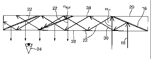
Fig. 2 illustrates a sectional view of an LOE according to the present
invention. The
first reflecting surface 16 is illuminated by a collimated display 18
emanating from a
light source (not shown) located behind the device. The reflecting surface I6
reflects
the incident light from the source such that the Iight is trapped inside a
planar
substrate 20 by total internal reflection. After several reflections from the
surfaces of
the substrate, the trapped waves reach an array of selectively reflecting
surfaces 22,
which couple the light out of the substrate into the eye of a viewer 24.
Assuming that
the central wave of the source is coupled out of the substrate 20 in a
direction normal
to the substrate surface 26, and the off axis angle of the coupled wave inside
the
substrate 20 is a;", then the angle aSUr2 between the reflecting surfaces and
the normal
to the substrate plane is:
(4)
asur~ = 2
As can be seen in Fig. 2, the trapped rays arrive at the reflecting surfaces
from
two distinct directions 28, 30. In this particular embodiment, the trapped
rays arrive
at the reflecting surface from one of these directions 28 after an even number
of
reflections from the substrate surfaces 26, wherein the incident angle (3rer
between the
trapped ray and the normal to the reflecting surface is:
o ° a~n (5)
~~~~f = 90 - (aa - as~~rz ) = 90 - 2
CA 02479824 2004-09-17
WO 03/081320 PCT/IL03/00237
The trapped rays arrive at the reflecting surface from the second direction 30
after an odd number of reflections from the substrate surfaces 26, where the
off axis
angle is a';n = 180°-a;" and the incident angle between the trapped ray
and the normal
to the reflecting surface is:
3a.
/j~rn.=90°-(a'a~-as~arz)=90°-(180°-arn-asura)=-
'~0°+ ~~
In order to prevent undesired reflections and ghost images, it is important
that
the reflectance be negligible for one of these two directions. The desired
discrimination between the two incident directions can be achieved if one
angle is
significantly smaller then the other one. Two solutions to this requirement,
both
exploiting the reflection properties of S-polarized light were previously
proposed,
however, both of these solutions suffer drawbacks. The main disadvantage of
the
first solution is the relatively large number of reflecting surfaces required
to achieve
an acceptable F~V. The main drawback of the second configuration is the
undesired
reflectance of the rays having an internal angle of a~n. An alternative
solution is
presently described, exploiting the reflection properties of P-polarized light
and in
some cases also the S-polarized Light, and providing for a shallower
reflecting surface
inclination so that fewer reflecting surfaces are required for a given
application.
The reflection characteristics as a function of incident angle of S- and
P-polarized light are different. . Consider for example an air/crown glass
interface;
while both polarizations reflect 4% at zero incidence, the Fresnel reflectance
of
S-polarized light incident on the boundary rises monotonically to reach 100%
at
grazing incidence, the Fresnel reflectance of P-polarized light first
decreases to 0% at
the Brewster's angle and only then rises to 100% at grazing incident.
Consequently,
one can design a coating with high reflectance fox S-polarized light at an
oblique
incident angle and near-zero reflectance for a normal incidence. Furthermore
one can
also readily design a coating for a P-polarized light with very Low
reflectance at high
incident angles and a high reflectance for Low incident angles. This property
can be
exploited to prevent undesired reflections and ghost images as described
above, by
CA 02479824 2004-09-17
WO 03/081320 PCT/IL03/00237
11
eliminating the reflectance in one of the two directions. For example choosing
(3Yef~ 25° from Equations (5) and (6) it can be calculated that:
~3'~.~~. =105° ; as =130° ; a'~» = 50° ; as~~ra =
65° . (7)
If now a reflecting surface is determined for which ~i're f 1S not reflected
but
~Yefis, the desired condition is achieved. Fig. 3A and 3B illustrate the
desired
reflectance behavior of selectively reflecting surfaces. While the ray 32
(Fig. 3A),
having an off axis angle of ~iref~.25°, is partially reflected and
coupled out of the
substrate 34, the ray 36 (Fig. 3B), which arrives at an off axis angle of
~i'ref~ 75° to
the reflecting surface (which is equivalent to ~i',.e~~ 105°), is
transmitted through the
reflecting surface 34 without any notable reflection.
Fig. 4 shows the reflectance curves of a dichroic coating designed to achieve
the above reflectance characteristics, for four different incident angles:
20°, 25°, 30°
and 75°, all of them for P-polarized light. While the reflectance of
the high-angle ray
is negligible over the entire relevant spectrum, the rays at off axis angles
of 20°, 2S°
and 30° obtain almost constant reflectance of 26%, 29% and 32%
respectively, over
the same spectrum. Evidently, reflectance decreases with the obliquity of the
incident
rays.
Fig. 5 illustrates the reflectance curves of the same dichroic coating, as a
function of the incident angle for P-polarized light with the wavelength
~,=550 nm.
Evidently, there are two significant regions in this graph: between 50°
and 80° where
the reflectance is very low and between 15° and 40° where the
reflectance increases
monotonically with decreasing incident angles. Hence, as long as, for a given
FOV,
one can ensure that the entire angular spectrum of J3'ref, where very low
reflections
are desired, will be located inside the first region while the entire angular
spectrum of
ref Where higher reflections are required, will be located inside the second
region
one can ensure the reflection of only one substrate modes into the viewer's
eye and
ensure a ghost-free image.
Up to now, only P-polarized light was analyzed. This treatment is sufficient
for a system using a polarized display source, such as a liquid-crystal-
display (LCD)
CA 02479824 2004-09-17
WO 03/081320 PCT/IL03/00237
12
or for a system where the output brightness is not crucial and the S-polarized
light
can be filtered out. However, for an unpolarized display source, like a CRT or
an
OLED, and where the brightness is critical, S-polarized light cannot be
neglected and
it must be taken into account during the design procedure. Fortunately,
although it is
more challenging than the P-polarized light, it is also possible to design a
coating
with the same behavior for an S-polarized light as discussed above. That is, a
coating
having a very low reflectance for an entire angular spectrum of ~i'r~ f and
higher,
pre-defined reflections for the respective angular spectrum of ~iref
Figs. 6 and 7 illustrate the reflectance curves of the same dichroic coating
described above with reference to Figs 4 and 5, but now fox S-polarized light.
Apparently, there are some differences between the behavior of the two
polarizations:
the region of high angles where the reflectance is very low is much narrower
for the
.S-polarization; it is much more difficult to achieve a constant reflectance
for a given
angle over the entire spectral bandwidth for the S-polarized light than for
the
P-polarized light; and finally, the monotonic behavior of the S-polarized
light at the
angular spectrum of ~i,.~f, where higher reflections are required, is opposite
to that of
the P-polarized light, that is, the reflectance for the S-polarized light
increases with
the obliquity of the incident rays. Apparently, this contradicting behavior of
the two
polarizations at the angular spectrum of ~3r~f could be utilized during the
optical
design of the system to achieve the desired reflectance of the overall light
according
to the specific requirements of each system.
It is clear that the reflectance of the first reflecting surface 16 (Fig. 2)
should
be as high as possible, so as to couple as much light as possible from the
display
source onto the substrate. Assuming that the central wave of the source is
normally
incident onto the substrate, i.e., cco = 180°, then the angle as~".1
between the first
reflecting surface and the normal to the substrate plane is:
GC,n + coo ~ a~~n -!"~o (g)
as~ur~ _ ~ ~ a s~u~n =
The solutions for asZ~r~ and CL'SUrI In the above example are 155°
and 115°,
respectively.
CA 02479824 2004-09-17
WO 03/081320 PCT/IL03/00237
13
Fig. 8 presents a sectional view of the reflective surface 16 which couples
light
38 from a display source (not shown) and traps it inside the substrate 20 by
total
internal reflection. As plotted here, the projection S~ of the reflecting
surface on the
substrate surface 40 is:
S, = T ~ tan(a) , ~ ~ (9)
wherein T is the substrate thickness.
The solution of a = CC'SUrI ~S preferred, since the coupling area on the
substrate
surface for the above example is more than 4.5 times larger than it is for the
previous
solutions. A similar improvement ratio holds for other systems. Assuming that
the
coupled wave illuminates the entire area of the reflecting surface, after
reflection
from the surface 16, it illuminates an area of 2S~ = 2T tan(a) on the
substrate surface.
On the other hand, the projection of a reflection surface 22 on the substrate
plane, is
SZ = T tan(asurz). To avoid either overlapping or gaps between the reflecting
surfaces,
the projection of each surface is adjacent to its neighbor. Hence, the number
N of
reflecting surfaces 22 through which each coupled ray passes during one cycle
(i.e.,
between two reflections from the same surface of the substrate) is:
N - 2Sj _ 2T ~ tan(czsuri ) , ( 10)
Sz T ~ tan(cz,urz
In this example, where ast~rz = 65° and CLszerl = 115°, the
solution is N = 2; that
is, each ray passes through two different surfaces during one cycle. This is a
conceptual change and a significant improvement over our previous disclosures,
where each ray passes through six different surfaces during one cycle. The
ability to
reduce the number of reflecting surfaces for a given FOV requirement relates
to the
projection of the reflecting surface on the viewing plane - as the angles in
the present
disclosure are larger, fewer reflection surfaces are needed. to span the image
dimensions. Allowing fewer reflection surfaces simplifies the implementation
of the
LOE and ensures a significant cost saving in its manufacture.
The embodiment described above with regard to Fig. 8 is an example of a
method fox coupling the input waves into the substrate. Input waves could,
however,
CA 02479824 2004-09-17
WO 03/081320 PCT/IL03/00237
14
also be coupled into the substrate by other optical means, including (but not
limited
to) folding prisms, fiber optic bundles, diffraction gratings, and other
solutions.
Also, in the example illustrated in Fig. 2, the input waves and the image
waves
are located on the same side of the substrate. Other configurations are
envisioned in
which the input and . the image waves could be located on opposite sides of
the
substrate. It is also possible, in certain applications, to couple the input
waves into
the substrate through one of the substrate's peripheral sides.
Fig. 9A is a detailed sectional view of an array of selectively reflective
surfaces which couple light trapped inside the substrate out and into the eye
of a .
viewer. As can be seen, in each cycle the coupled ray passes through
reflecting
surfaces 42, having a direction of a'~n = 130°, whereby the angle
between the ray and
the normal to the reflecting surfaces is ~75° and the reflections from
these surfaces
are negligible. In addition, the ray passes in each cycle twice through the
reflecting
surface 44 having a direction, of a;" = 50°, where the incident angle
is 25° and part of
the ray's energy is coupled out of the substrate. Assuming that one array of
two
selectively reflecting surfaces 22 is used to couple the light onto the
viewer's eye, the
maximal FOV is:
2T tan gs.",., - chye ~ ( 11 )
FOVm
Re~e
Hence, for the same parameters of the examples above, the limiting substrate
thickness for an FOV of 8° is in the order of 2.8 mm; for FOVs of 1
S° and 30°, the
limiting substrate thickness is 3.7 mm and 5.6 mm, respectively. These are
more
favorable values than the limiting thickness of the state-of the-art solutions
discussed
above. Moreover, more than two selectively reflecting surfaces can be used.
For
example, for three selectively reflecting surfaces 22, the limiting substrate
thickness
for FOVs of 15° and 30° is approximately 2.4 mm and 3.9 mm,
respectively.
Similarly additional reflecting surfaces may be introduces to, amongst other
advantages, reduce the limiting optical thickness further.
For configuration where a relatively small FOV is required, a single partially
reflecting surface can be sufficient. For example, fox a system with the
following
CA 02479824 2004-09-17
WO 03/081320 PCT/IL03/00237
parameters: Reye = 25 mm ; ocsttr = 72° and T-- 5 mm, a moderate FOV of
17° can be
achieved even with a single reflecting surface 22. Part of the rays will cross
the
surface 22 several times before being coupled out into the desired direction.
Since
the minimal propagation angle inside the substrate to achieve the total-
internal
reflection condition for BK7 material or similar is a;n~,n;"> = 42°,
the propagation
direction of the central angle of the FOV 1S CGin(cen) = 48°.
Consequently, the
proj ected image is not normal to the surface but is rather inclined to
12° off axis.
Nevertheless, far many application this is acceptable.
As illustrated in Fig. 9B, each selectively reflecting surface is illuminated
by
optical rays of different intensities. While the right surface 46 is
illuminated by rays
immediately after they are reflected from the lower face 48 of the substrate
20, the
left surface 50 is illuminated by rays that have already passed through the
partially
reflecting surface 46 and therefore have lower intensity. To achieve images of
uniform brightness, compensation is required, for the differences in
intensities
between the different portions of the image. Indeed, coating the reflecting
surfaces
with different coatings, whereby the reflectance of surface 46 is lower than
the
reflectance of surface 50 compensates for the uneven illumination.
Another potential non-uniformity in the resulting image might occur due to the
different reflection sequences of different rays that reach each selectively
reflecting
surface:-some rays arrive directly without a reflection from a selectively
reflecting
surface; other rays arrive after one or more such reflections. This effect is
illustrated
in Fig. 9A. A ray intersects the first selectively reflecting surface 22 at
the point 52.
The incident angle of the ray is 25° and a portion of the ray's energy
is coupled out
of the substrate. The ray then intersects the same selectively reflecting
surface at
point 42 at an incident angle of 75° without noticeable reflection, and
then intersects
again at point 54 at an incident angle of 25° where another portion of
the ray's
energy is coupled out of the substrate. In contrast the ray shown in Fig. 9B,
experiences only one reflection from the same surface. We note that more
multiple
reflections occur at smaller incident angles. Therefore, one method to
compensate for
non-uniformity that results from such multiple-intersections is to design a
coating
CA 02479824 2004-09-17
WO 03/081320 PCT/IL03/00237
16
where the reflectance increases monotonically with decreasing incident angle,
as
shown in the reflectivity for the range 10-40° of Fig. 5. It is
difficult to fully
compensate for such differences in multiple-intersection effects.
Nevertheless, in
practice, the human eye tolerates significant variations in brightness which
remain
unnoticed. For near-to-eye displays, the eye integrates all the light which
emerges
from a single viewing angle and focuses it onto one point on the retina, and
since the
response curve of the eye is logarithmic, small variations, if any, in the
display's
brightness will not be noticeable. Therefore, even for moderate levels of
illumination
uniformity within the display, a human eye experiences a high-quality image.
The
required moderate uniformity can readily be achieved with an LOE.
For displays located at a distance from the eye, however, like head-up
displays, the non-uniformity due to the multiple intersection effects cannot
be
tolerated. For these cases, a more systematic method to overcome the non-
uniformity
is required. Figure 10 illustrate one possible approach. A thin transparent
layer 55
with a thickness Tad is cemented at the bottom of the LOE. In this
arrangement, the
exemplary ray incident at 25°, which according to Fig. 9A intersected
the first
selectively reflecting surface 22 at three.points, intersects this surface
only twice and
is reflected only once: at the point 52. In this manner, the double-reflection
effect
does not occur. The thickness Tad can be calculated to minimize the
double-reflection effect for the entire FOV of the optical system. For
example, for
optical system having the following parameters: FOV = 24° ; asZtr =
64° ; a;n = 52°;
v=1.51 and T 4 mm, a layer with a thickness of T°~~ =.2.1 mm should be
added to
totally eliminate the undesired double-pass effect. Evidently, the total
thickness of
the LOE is now 6.1 mm instead of 4 mm, but fox HUD systems where the combiner
is relatively large and a mechanical strength is required for the LOE, the
increased
thickness is not necessarily a drawback. It is possible to add the transparent
layer at
the top of the LOE or even on both sides of the substrate, wherein the exact
configuration will be set according to the specific requirements of the
optical system.
For the proposed configuration, no matter what the thickness of T~,d~ is, at
least some
of the rays intersect the same selectively reflecting surface twice. For
instance, in
CA 02479824 2004-09-17
WO 03/081320 PCT/IL03/00237
17
Fig. 10, the ray passes once through the first reflecting surface 22 at the
point 52
having an incident angle of 25° where part of the ray's energy is
coupled out of the
substrate, and once at an incident angle of 75° without noticeable
reflection.
Naturally, only the first intersection contributes to the image which is
formed by the
LOE.
In considering the viewing angles different portions of the resulting image
originate at different portions of the partially reflecting surfaces, Fig. 11
illustrates
this effect: a sectional view of a compact LOE display system based on the
proposed
configuration. Here a single plane wave 56, representing a particular viewing
angle
~, illuminates only part of the overall array of partially reflecting surfaces
22. Thus,
fox each point on the partially reflecting surface, a nominal viewing angle is
defined,
and the reflectance is designed according to this angle.
The ~ design of the coatings of the various partially reflective surfaces of
the
LOE is performed as follows: For each particular angle, a ray is plotted
(taking into
account the refraction due to Snell's Law) from the center of the designated
eye pupil
60 to' the partially reflecting surface. The calculated direction is set as
the nominal
incident direction and the particular coating is designed according to that
direction,
by also taking into account prior reflectance related to this particular
viewing angle.
Hence, for each viewing angle, the average reflectance from the relevant
surfaces will
be very close to the desired reflectance, In addition, if required, a layer
with a
thickness TQ~~will be added to the LOE,
An LOE with non-identical selectively reflecting surfaces has two
consequences. In see-through systems, such as head-mounted displays for
pilots,
wherein the viewer should see the external scene through the LOE so the
reflectance
of the selectively reflecting surfaces should be relatively high. Since here
the
reflectance coefficient is not the same for all the selectively reflecting
surfaces, there
is a danger that this would also entail a non-uniform image of the external
scene
viewed through the substrate. Fortunately, this non-uniformity is rather
small, and
can be neglected in many cases. In other situations, where such potential non
uniformity is crucial, a complementary non-uniform coating could be added on
the
CA 02479824 2004-09-17
WO 03/081320 PCT/IL03/00237
external surface of the substrate, to compensate for the non-uniformity of the
substrate and to achieve a view of uniform brightness over the entire FOV.
In non-see-through systems, such as virtual-reality displays, the substrate is
opaque and the transmittance of the system has no importance. However, in such
a
case, the reflectance may be rather higher than before, and care must be taken
in
order to ensure that enough intensity passes through the first reflecting
surface in
order to achieve a uniform brightness across the entire FOV. Another issue
that
should be taken into account is the polarization of the light. As discussed
above, for
the selectively reflecting surface Boating, P-polarized light is preferred.
Fortunately,
some of the compact display sources (e.g., nematic liquid crystal displays)
are
linearly polarized. This would also apply to situations where the display
source is
oriented such that the incoming light is S-polarized in relation to the
reflective
surfaces. In such cases it is possible to either design a coatings for the S-
polarized
light, or, alternatively rotate the ~ source's polarization with a half wave
plate. As
illustrated in Fig. 12, the light emerging from the display source 4 is
linearly
S-polarized. By using a half wave plate 62, the 'polarization is rotated so
that the
desired P-polarized light is incident onto the coupling reflective surface 22.
To illustrate the expected performance of a typical see-through system, a
computer simulation has been performed, calculating the brightness of both the
projected display and the external scene. The system has the following
parameters:
T = 4.3 mm ; T~~~ = 0 ; oc;" = 50° ; FOV = 24° ; Rye = 25 mm;
v=1.51; the display
source is S-polarized, there are two selectively reflecting surfaces, and the
nominal
reflectance is 22%. Fig. 13 shows the simulation results, normalized to the
requested
nominal values. There are some small fluctuations in both graphs, but these
changes
would no be noticeable in near-to-eye applications.
Thus far, only the FOV along the ~ axis has been discussed. The FOV along
the orthogonal r~ axis should also be considered. The FOV along the r~ axis is
not
dependent upon the size or number of the selectively reflecting surfaces, but
rather,
on the lateral dimension along the r~ axis of the input waves coupled into the
substrate. The maximum achievable FOV along the r~ axis is:
CA 02479824 2004-09-17
WO 03/081320 PCT/IL03/00237
19
D,~ - d~y~ (I2)
FOVmax ~ Rey' + 1 l(v sin a;n ) '
wherein D~ is the lateral dimension along r~ axis of the input waves coupled
into the
substrate.
That is, if the desired FOV is 30°, then by using the same parameters
described
above, the limiting lateral dimension is 42 mm. It was previously demonstrated
that
the longitudinal dimension along the ~ axis of the input waves coupled into
the
substrate is given by SI = T tan(a,;n). A substrate thickness of T = 4 mm
yields
SI = ~.6 mm. Seemingly, the lateral extent of the LOE is fivefold larger than
the
longitudinal dimension. Even for an image aspect ratio of 4:3 (as with a
standard
video display) and the FOV in the ~ axis is 22°, the required lateral
dimension is
approximately 34 mm, still four-fold larger than the longitudinal dimension.
This
asymmetry is problematic:- a collimating lens with a high numerical aperture,
or a
very large display source are. required. In any case, with such numerical
values
dimensions, it is impossible to achieve the desired compact system.
An alternative method for solving this problem is presented in Fig. 14.
Instead
of using ,an array of reflecting surfaces 22 only along the ~ axis, another
array of
reflecting surfaces 22a, 22b, 22c, 22d is positioned along the r~ axis. These
reflecting
surfaces are located normal to the plane of substrate 20 along the bisector of
the ~ and
r~ axes. The reflectance of these surfaces is determined so as to achieve
uniform
output waves. For example, for four reflecting surfaces, the reflectance of
the
surfaces should be 75%, 33%, 50% and 100% for the first surface 22a, the
second
surface 22b and the third surface 22c, and the fourth surface 22d,
respectively. This
arrangement yields a sequence of wavefronts, each at 25% of the incoming
intensity.
Typically, such an array of reflecting surfaces can be readily designed for S-
polarized
light. Fortunately, the light which is S-polarized compared to the partially
reflecting
surfaces 22a-22d, will be P-polarized compared to the partially reflecting
surfaces 22.
Therefore, if the vertical expansion of the image in the rl axis is affected
with
S-polarized light, there is no need for a half wavelength plate to rotate the
CA 02479824 2004-09-17
WO 03/081320 PCT/IL03/00237
polarization of the light onto the horizontal expanders in the ~ axis. The
arrangements shown in, the array assemblies 22 and 22a-22d are only examples.
Other arrangements for increasing the lateral dimensions of the optical waves
in both
axes, in accordance with the optical system and the desired parameters, are
possible,
some of which are described below.
Figure 15 illustrates an alternative method to expand the beam along the r~
axis. In this configuration the reflectance of surfaces 22a, 22b and 22c is
50% for
S-polarized light where 22d is a simple 100% mirror. Although the lateral
dimension
of the vertical expansion for this solution is larger than the previous
configuration, it
requires only one simple selectively reflecting coating and the overall
configuration is
easier to fabricate. In general, for each specific optical system the exact
method to
expand the beam along the r~ axis can be chosen according to the particular
requirements of the system.
Assuming a symmetrical collimating lens 6, the lateral dimension along. the r~
axis after the reflection from the reflective surfaces 22a-22d, is given by
S,~ = NT tan(ain), wherein N is the number, of the reflecting surfaces. The
maximum
achievable FOV along the r~ axis is now:
S,~ - d~y~ NT tan(a;" ) - deye (13)
FOI~max ~ ReYc + l l(v sin a;" ) Reye + l l(v sin a;n )
Since the reflecting array 22a-22d can be located closer to the eye, it is
expected that the distance l between the reflecting surfaces will be smaller
than in
previous examples. Assuming that l = 40 mm, and choosing the parameters: T = 4
mm ; N= 4; a;,~ = 65°; Reye = 25 mm and v = 1.5, the resultant FOV will
be:
FOhmax ~ 30° . ' (14)
This is an improvement with respect to the previous values obtained above.
Figure 16 illustrates another method to expand the beam along both axes
utilizing a double LOE configuration. The input wave is coupled into the first
LOE
20a by the first reflecting surface 16a and then propagating along the ~ axis.
The
partially reflecting surfaces 22a couple the light out of 20a and then the
light is
CA 02479824 2004-09-17
WO 03/081320 PCT/IL03/00237
21
coupled into the second LOE 20b by the reflecting surface 16b. The light is
then
propagates along the r~ axis, and then coupled out by the selectively
reflecting
surfaces 22b. As shown, the original beam is expanded along both axes where
the
overall expansion is determined by the ratio between the lateral dimensions of
the
elements lba and 22b respectively. The configuration given in Fig. 16 is just
an
example of a double-LOE setup. Other configurations where two or more LOEs are
.
combined together to form complicated optical systems are also possible. For
example, three different substrates, the coating of each being designed for
one of the
three basic colors, can be combined to produce a three-color display system.
In that .
case, each substrate is transparent with respect to the other two colors. Such
a system
can be useful for applications in which a combination of three different
monochromatic display-sources is required in order to create the final image.
There
are many other examples in which several substrates can be combined together
to
form a more complicated system.
Another issue to be addressed is the brightness of the system. This issue is
important for see-through applications, where it is desired that the
brightness of the
display will be comparable to that of the external scene, to allow acceptable
contrast
ratio and convenient observation through the combiner. It is not possible to
ensure
that the insertion loss of most of the systems is small. For example, as
described
above for the four-surface combiner of Fig. 14, because of the requested beam
expansion along the r~ axis, the brightness of the optical waves is reduced
four-fold.
In general for N-reflecting surfaces the brightness reduces by a factor of N.
In
principle high-brightness display sources can offset this difficulty, but this
approach
necessarily has a practical limitation. Not only are high-brightness display
sources
very expensive, they also have high power consumption with the associated very
high
electrical currents. Furthermore, in most of the displays there is an inherent
limitation to the maximal brightness that can be achieved. As . an example,
for
transmission LCDs, which are presently the most abundant source for small
displays,
the baclc-illumination light power is limited to avoid undesired effects lilce
flaring
CA 02479824 2004-09-17
WO 03/081320 PCT/IL03/00237
22
which decrease the resolution and contrast ratio of the display. Therefore,
other
approaches are required to optimize the use of the available light from the
source.
One possible method to improve the brightness of the display which reaches
the viewer's eye is to control the reflectance of the reflecting surfaces 22
of the LOE
according to the eye-motion-box (EMB) of the viewer. As illustrated in Fig.
11, each
reflecting surface of the overall array of selectively reflecting surfaces 22,
is
illuminated by only the part of the overall FOV. Hence, the reflectance of
each
surface can be set to optimize the brightness of the entire FOV. For example,
the
reflectance of the right surface 22a in Fig. 11 could be designed to have
higher
reflectance for the right part of the FOV and the lowest possible reflectance
for the
left part of the FOV, while the left surface 22b have higher reflectance for
the left
part of the FOV. A similar design method can be applied to a two-dimensional
expansion system. Assuming that r~ is the vertical axis in Fig. 16, the
reflectance of
the reflecting surfaces 22a could be designed such that the lower surfaces
will have
higher reflectance for the lower part of the FOV and the lowest possible
reflectance
for the higher part of the FOV, while the upper surfaces have higher
reflectance for
the upper part of the FOV. Therefore, the factor in which the brightness is
reduced
because of the lateral expansion can be much smaller than R, where R is the
ratio
between the area of the coupling-in surface 16a and the coupling-out surfaces
22b.
Another method to improve the overall brightness of the system is by
controlling the display source brightness without changing the input power. As
shown in Fig. 11 above, a large portion of the energy coupled onto the
substrate 20 by
the reflecting mirror 16 is reflected into the vicinity of the eye pupil 60.
To maximize
the achievable brightness, however, it is also desirable that most of the
light that
emerges from the display source couples into the substrate.
Figure 17 illustrates an example of a substrate-mode display where the display
source is a transmission LCD. The light which emerges from the light source 64
and
collimated by a lens 66, illuminates an LCD 68. The image from the LCD is
collimated and reflected by the optical components 70 onto the substrate 20.
Figure
18 illustrates . an optical layout of the collimating/folding lens 70, while
Fig. 19
CA 02479824 2004-09-17
WO 03/081320 PCT/IL03/00237
23
illustrates the foot-print of the light, which is coupled into the substrate
20, on the
front surface 72 of the lens 70. Usually, for most of the display source,
there is a
Lambertian distribution of the light, which emerges from the display. That is,
the
energy is distributed uniformly over the entire angular spectrum of 2~c
steradians. As
can be seen in Figs. 18 and 19, however, only a small portion of the light
which
emerges from the display source is actually coupled into the substrate 20.
From each
point source on the display surface, only a small cone of light of ~20-
30° actually
illuminate the footprint on the front surface 72 and couples into the
substrate 20.
Therefore, a significant increase in the brightness can be achieved if the
light which
emerges from the display is concentrated inside this cone.
One method to achieve such directionality in the source illumination is to use
a
special selective diffuser for the LCD. Usually, a conventional diffuser
scatters the
light uniformly in all directions. Alternatively, a selective diffuser can
spread the
light in such a way that the light from each point source diverges into a~
required
angular cone. In this case the power that the LCD surface illuminates remains
the
same. For a 20-30° cone, the diverging angle of the light for each
point source is
reduced by a factor of more than 50 as compared to the ~ steradians of the
Lambertian source, the brightness of the light increases by the same factor.
Hence, a
significant improvement in the brightness of the system can be achieved with a
minimal design and manufacturing effort and without increasing the power
consumption of the system.
An alternative solution, which is appropriate not only to LCDs but also to
other display sources, is to use an array of micro-lenses that is aligned with
the pixels
of the display source. For each pixel a micro-lens narrows the diverging beam
that
emerges from that pixel into the desired angular cone. In fact, this solution
is
efficient only if the fill-factor of the pixels is a small number. An improved
version
of this solution is to design the emitting distribution function of the pixels
in the
pixel-array to make each pixel diverge into the required angle. For example,
in
OLED displays, efforts are usually made to increase the divergence angle of
the
single LEDs in order to allow viewing from a wide angle. For our specific LOE
CA 02479824 2004-09-17
WO 03/081320 PCT/IL03/00237
24
display application, however, it is advantageous to keep this divergence angle
small,
in the order of 20-30°, to optimize the brightness of the system.
As described above with a reference to Figs. 14 and 15, it is possible to
achieve a wide FOV also along the vertical r~ direction without increasing the
volume
of the system significantly. There are, however, situations where this
solution is not
sufficient. This is true especially for systems with a very wide FOV and a
constraint
on the distance, l,, between the couple-in reflective surface 16 and the
couple-out
selectively reflecting surfaces 22. Figure 20 illustrates an unfolded optical
system
with the following parameters: l = 70 mm ; T= 4 mm ; cc;n = 65°; Reye =
24 mm ;
v = 1.51, the eye-motion-box (EMB) is 10 mm and the required vertical FOV is
42°.
If we trace the rays from the EMB 74, we find that the light passes through
the
projection of the EMB on the couple-out optics 22, where 76, 78 and 80 are the
projections of tie upper, central and lower angles, respectively of the FOV.
This
means that to achieve the desired FOV the required couple-in aperture 82 is 65
mm;
this is a very large aperture that necessarily increases the size of the
entire system,
even if the substrate remains a thin plate. Alternatively, if only a smaller
aperture 84
of 40 mm is allowed, the achievable vertical FOV 86 falls to 23° which
is nearly half
of the required FOV.
Figure 21 illustrates a possible solution to this problem. Instead of using a
simple rectangular plate 20, the two horizontal edges of the plates are
replaced with
two pairs of parallel reflecting surfaces, 88a, 88b and 90a, 90b respectively.
While
the central part of the FOV projects directly through to the aperture 84 as
before, the
rays from the lower part of the FOV are reflected from surfaces 88a and 88b,
while
the rays from the upper part of the FOV are reflected from surfaces 90a and
90b.
Typically, the angles between the rays trapped inside the substrate and the
reflecting
surfaces 88 and 90 are sufficiently large to affect total internal
reflections, so no
special reflecting coating is required for these surfaces. Since aII rays are
either
traveling directly from the input aperture or reflected twice from a pair of
parallel
surfaces, the original direction of each xay is maintained, and the original
image is not
affected.
CA 02479824 2004-09-17
WO 03/081320 PCT/IL03/00237
Indeed, it is important to ensure that each ray which is reflected by surface
88a
is also reflected by surface 88b before it impinges on aperture 84. To confirm
this, it
is sufficient to check two rays paths:- the marginal ray of the extreme angle
92,
incident on surface 88a at the point 94, must impinge on surface 88b to the
right of its
intersection with surface 90a; in addition; the marginal ray 96, incident on
surface
88a next to its intersection 98 with surface 90b, must impinge on surface 88b
before it
crosses the aperture 84. As both marginal rays meet the requirement,
necessarily all
rays from the FOV that are incident on surface 88a will also impinge on
surface 88b.
The present example provides for an FOV of 42° with a significantly
reduced input
aperture 84: 40 mm. Naturally, in cases where l is extremely large, a cascade
of two
or more pairs of reflecting surfaces can be used to achieve the desired FOV
while
maintaining an acceptable input aperture.
The embodiment of Fig. 21 is just an example 'illustrating a simple
implementation of this method. The use of pairs of parallel reflecting
surfaces in
order to decrease the aperture of the system for a given FOV, or alternatively
to
increase the useable FOV for a given aperture, is not limited to substrate-
mode optics
and it can be utilized in other optical systems including, but not limited to,
free-space
systems like head-up displays, episcops or periscopes.
Apparently, as described above with reference to Fig. 21, the lateral
dimension
of the input aperture of the substrate is 40 mm along the r~ axis and 8.5 mm
along the
~ axis. Figures 22A and 22B illustrate an alternative embodiment to that
described
above with reference to Figs. 14-15. This approach involves an adjustment
between a
symmetrical collimating lens 6 and an asymmetrical input aperture. The lateral
dimensions of the input aperture are assumed to be D and 4D along the two axes
respectively. A lens 6 with an aperture of 2D collimates the image onto the
substrate.
The front half of the collimated light is coupled into the substrate by the
mirror 16a.
Two pairs of parallel reflecting surfaces, 22a; 22b and 22c; 22d split the
coupled light
outward and then reflects it back to its original direction. The rear part of
the
collimated light passes through the substrate 20 and then folded by the prism
99 back
into the substrate. A second mirror 16b couples the folded light onto the
substrate 20.
CA 02479824 2004-09-17
WO 03/081320 PCT/IL03/00237
26
Evidently, the lateral dimensions of the input aperture are D and 4D along the
two
axes respectively, as required.
There are some advantages to the approach describe above with reference to
Fig. 22. The system is symmetrical about the rl axis and more important, there
is no
loss of light intensity. This approach is only an example and other similar
methods to
convert the symmetrical input beam into an asymmetrical coupled light beam are
possible. A suitable conf guration for expanding the image along the r~ axis
requires
careful analysis of the system specifications.
In general, all the different configurations of the light-guide optical
elements
considered above, offer several important advantages over alternative compact
optics
fox display applications, which include:
1) The input display source can be located very close to the substrate, so
that the
overall optical system is very compact and lightweight, offering an
unparalleled
form-factor.
2) In contrast to other compact display configurations, the present invention
offers flexibility as to location of the input display source relative to the
eyepiece.
This flexibility, combined with the ability to locate the source close to the
expanding
substrate, alleviates the need to use an off axis optical configuration that
is common
to other display systems. In addition, since the input aperture of the LOE is
much
smaller than the active area of the output aperture, the numerical aperture of
the
collimating lens 6 is much smaller than required for a comparable conventional
imaging system. Consequently a significantly more convenient optical system
can be
implemented and the many difficulties associated with off axis optics and high
numerical-aperture lenses, such as field or chromatic aberrations can be
compensated
for relatively easily and efficiently.
3) The reflectance coefficients of the selectively reflective surfaces in the
present
invention are essentially identical over the entire relevant spectrum. Hence,
both
monochromatic and polychromatic, light sources may be used as display sources.
The LOE has a negligible wavelength-dependence ensuring high-quality color
displays with high resolutions.
CA 02479824 2004-09-17
WO 03/081320 PCT/IL03/00237
27
4) Since each point from the input display is transformed into a plane wave
that is
reflected into the eye of the viewer from a large part of the reflecting
array, the
tolerances on the exact location of the eye can be significantly relaxed. As
such, the
viewer can see the entire field-of view, and the eye-motion-box can be
significantly
larger than in other compact display configurations.
5) Since a large part of the intensity from the display source is coupled into
the
substrate, and since a large portion of this coupled energy is "recycled" and
coupled
out into the eye of the viewer, a display of comparatively high brightness can
be
achieved even with display sources with low power consumption.
Figure. 23 illustrates an embodiment of the present invention in which the
LOE 20 is embedded in an eye-glasses frame I00. The display source 4, the
collimating Lens 6,, and the folding lens 70 are assembled inside the arm
portions 102
of the eye-glasses frame, just next to the edge of the LOE 20. For a case in
which the
display source is an electronic element such as a small CRT, LCD, or OLED, the
driving electronics 104 for the display source might be assembled inside the
baclc
portion of the arm 102. A power supply and data interface 106 is connectable
to arm
102 by a Iead 108 or other communication means including radio or optical
transmission. Alternatively, a battery and miniature data link electronics can
be
integrated in the eye-glasses frame.
The embodiment described above can serve in both see-through and
non-see-through systems. In the latter case opaque layers are located in front
of the
LOE. It is not necessary to occlude the entire LOE, typically only the active
area,
where the display is visible needs to be blocked. As such, the device can
ensure that
the peripheral vision of the user is maintained, replicating the viewing
experience of a
computer or a television screen, in which such peripheral vision serves an
important
cognitive function. Alternatively, a variable filter can be placed in front of
the system
in such a way that the viewer can control the level of brightness of the light
emerging
from the external scene. This variable filter could be either a mechanically
controlled
device such as a folding filter, or two rotating polarizers, an electronically
controlled
CA 02479824 2004-09-17
WO 03/081320 PCT/IL03/00237
28
device, or even an automatic device, whereby the transmittance of the filter
is
determined by the brightness of the external background.
There axe some alternatives as to the precise way in which an LOE can be
utilized in this embodiment. The simplest option is to use a single element
for one
eye. Another option is to use an element and a display source for each eye,
but with
the same image: Alternatively it is possible to project two different parts of
the same
image, with some overlap between the two eyes, enabling a wider FOV. Yet
another
possibility is to project two different scenes, one to each eye, in order to
create a
stereoscopic image. With this alternative, attractive implementations are
possible,
including 3-dimensional movies, advanced virtual reality, training systems and
others.
The embodiment of Fig. 23 is just an example illustrating the simple
implementation of the present invention. Since the substrate-guided optical
element,
constituting the core of the system, is very compact and lightweight, it could
be
installed in a vast variety of arrangements. Hence, many other embodiments are
also
possible including a visor, a folding display, a monocle, and many more. This
embodiment is designated for applications where the display should be near-to-
eye:
head-mounted, head-worn or head-carried. There are, however, applications
where
the display is located differently. An example of such an application is a
hand-held
device for mobile application, such as for example a cellular phone: These
devices
are expected in the near future to perform novel operations, which require
the,
resolution of a large screen, including videophone, Internet connection,
access to
electronic mail, and even the transmission of high-quality television
satellite
broadcasting. With the existing technologies, a small display could be
embedded
inside the phone, however, at present, such a display can project either video
data of
poor quality only, or a few lines of Internet or e-mail data directly into the
eye.
Figure 24 illustrates an alternative method, based on the present invention,
which eliminate the current compromise between the small size of mobile
devices
and the desire to view digital content on a full format display, by projecting
high
quality images directly into the eye of the user. An optical module including
the
CA 02479824 2004-09-17
WO 03/081320 PCT/IL03/00237
29
display source 6, the folding and collimating optics 70 and the substrate 20
is
r
integrated into the body of a cellular phone 110, where the substrate 20
replaces the
existing protective cover-window of the phone. Specifically, the volume of the
support components including source 6 and optics 70 is sufficiently small to
fit inside
the acceptable volume for modern cellular devices. To view the full screen
transmitted by the device the user positions the window in front of his eye
24, to
conveniently view the image with high FOV, a large eye-motion-box and a
comfortable eye-relief. It is also possible to view the entire FOV at a larger
eye-relief
by tilting the device to display different portions of the image. Furthermore,
since the
optical module can operate in see-through configuration, a dual operation of
the
device is possible; namely it is optionally possible to maintain the
conventional
cellular display 112 intact. In this manner the standard, low-resolution
display can be
viewed through the LOE when the display source 6 is shut-off. In a second
mode,
designated for e-mail reading. Internet surfing, or video operation, the
conventional
display 112 is shut-off while the display source 6 projects the required wide
FOV
image into the viewer's eye through the LOE. The embodiment described in Fig.
24
is only an example, illustrating that applications other than head-mounted-
displays
can be materialized. Other possible hand-carried arrangements include palm
computers, small displays embedded into wristwatches, a pocket-carried display
having the size and weight reminiscent of a credit card, and many more.
The embodiments described above are mono-ocular optical systems, that is,
the image is projected onto a single eye. There are, however, applications,
such as
head-up displays (HUD), wherein it is desired to project an image onto both
eyes.
Until recently, HUD systems have been used mainly in advanced combat and
civilian
aircraft. There have been numerous proposals and designs, of late, to install
a HUD
in front of a car driver in order to assist in driving navigation or to
project a thermal
image into his eyes during low-visibility conditions. Current aerospace HUD
systems
are very expensive, the price of a single unit being ~in the order of hundreds
of
thousands of dollars. In addition, the existing systems are very large, heavy,
and
bullcy, and axe too cumbersome for installation in a small aircraft let alone
a car.
CA 02479824 2004-09-17
WO 03/081320 PCT/IL03/00237
30 '
LOE-based HUD potentially provide the possibilities for a very compact,
self contained HUD, that can be readily installed in confined spaces. It also
simplifies
the construction and manufacturing of the optical systems related to the HUD
and
therefore is a potentially suitable for both improving on aerospace HUD's, as
well as
introducing a compact, inexpensive, consumer version for the automotive
industry.
Fig. 25 illustrates a method of materializing an HUD system based on the
present invention. The light from a display source 4 is collimated by a lens 6
to
infinity and coupled by the first reflecting surface 16 into substrate 20.
After
reflection at a second reflecting array (not shown), the optical waves impinge
on a
third reflecting surfaces 22, which couples the light out into the eyes 24 of
the viewer.
The overall system can be very . compact and lightweight, of the size of a
large
postcard having a thickness of a few millimeters. The display source, having a
volume of a few cubic centimeters, can be attached to one of the corners of
the
substrate, where an electric wire can transmit the power and data to the
system. It is
expected that the installation of the presented HUD system will not be more
complicated than the installation of a simple commercial audio system.
Moreover,
since there is no need for an external display source for image projection,
the
necessity to install components in unsafe places is avoided.
Since the exit pupil of a typical HUD system is much larger than that of a
head-mounted system, it is expected that a three-array configuration, as
described
above with reference to Figs. 14-16, will be needed to achieve the desired FOV
There may be some special cases, however, including systems with small
vertical
FOVs, or with a vertical LED array as a display source, or by exploiting pairs
of
parallel reflecting mirrors (as described above with reference to Fig. 21) in
which a
two-array configuration would suffice.
The embodiments illustrated in Fig. 25 can be implemented for other
applications, in addition to HUD systems for vehicles. One possible
utilization of
these embodiments is as a flat display for a computer or television. The main
unique
characteristic of such a display is that the image is not located at the
screen plane, but
is focused at infinity or to a similarly convenient distance. One of the main
CA 02479824 2004-09-17
WO 03/081320 PCT/IL03/00237
31
drawbacks of existing computer displays is that the user has to focus his eyes
at a
very close distance of between 40 and 60 cm, while the natural focus of a
healthy eye
is to infinity. Many people suffer from headaches after worlcing for a long
duration
of time at a computer. Many others who work frequently with computers tend to
develop myopia. In addition, some people, who suffer from both myopia and
hyperopia, need special spectacles for work with a computer. A flat display,
based on
the present invention, could be an appropriate solution for people who suffer
from the
above-described problems and do not wish to work with a head-mounted display.
Furthermore, the present invention allows for a significant reduction in the
physical
size of the screen. As the image formed by the LOE is larger than the device,
it
would be possible to implement large screens on smaller frames.. This is
particularly
important for mobile applications such as lap and palm-top computers.
One potential problem that might arise with a large display LOE relates to its
brightness. Ideally, for compactness it is advantageous to use a miniature
display
source, but this necessarily reduces the display brightness due to the large
increase in
the actively illuminated area of the LOE as Compared to the actively
illuminated area
of the source. Therefore, even after the special measures described in the
foregoing
are deployed, one expects a reduction in the brightness, even for non- see
through
applications. This reduction .in the brightness can be offset either by
increasing the
brightness of the source, or deploying more than one source. That is, the LOE
can be
illuminated with an array of display sources and their associated collimating
lenses.
Fig. 26 illustrates an example of this method. The same image is generated
from an
array of 4 display sources 4a through 4d, each collimated by a related array
of lenses
6a, through 6d to form a single collimated image, which is coupled into the
LOE 20
by the reflecting surface 16. At a first glance it loops like this solution
can be quite
expensive. Here any increased system cost through increase in its components
and
the need to coordinate the sources images with special electronics is offset
by the
inherently low cost of the micro-displays themselves and the ability to reduce
the
numerical aperture of the collimating lenses. There is also no need for a
lateral
expander in this arrangement; it is quite feasible to include only a one-
dimensional
CA 02479824 2004-09-17
WO 03/081320 PCT/IL03/00237
32
image expander LOE and increase the brightness accordingly. It is important to
note
that the display sources should not necessarily be identical to each other and
a more
complicated system with a different display sources can be utilized as
explained in
what follows.
Another advantage of the LOE display of the present invention is its very flat
shape, even compared to the existing flat-panel displays. Another. difference
is a
significantly more directional viewing angle: the LOE display can be viewed
from a
significantly limited angular range as compared to common flat-panel display.
Such
limited head-motion-box is sufficient for convenient operation by a single
user, and
offers the additional advantages of privacy in many situations.
Furthermore, the image of the LOE-based screen is located in a distant plane
behind the display surface and not on its physical surface. The sensation of
the image
is similar to viewing it through a window. This configuration is particularly
suitable
for implementing three-dimensional displays.
Ongoing developments in information technology have led to an increasing
demand for 3-D displays. Indeed, a broad range of 3-D equipment is already on
the
market. The available systems, however, suffer from the drawback that users
are
required to wear special devices to separate images intended for the left eyes
and the
right eye. Such "aided viewing" systems have been firmly established in many
professional applications. Yet further expansion to other fields will require
"free
viewing" systems with improved viewing comfort and closer adaptation to the
mechanisms of binocular vision. The present solutions to this problem suffer
from
various disadvantages and fall behind familiar 2-D displays in terms of image
quality
and viewing comfort.
Figures 27A and 27B illustrate a front view and a top view, respectively, of a
possible configuration, based on the present invention to materialize a real 3-
D
display. Instead of a single display source, an array 114 of h different
display sources
1141 114" is located 'at the lower portion of the substrate 20, where each
display
source projects images obtained at different perspectives of the same scene.
The
image from each display source is coupled into the substrate in the same
manner as
CA 02479824 2004-09-17
WO 03/081320 PCT/IL03/00237
33
described above with reference to Fig. 26. When the viewer is observing the
display,
his right 24a and left 24b eyes view the images projected from the display
sources
114i and 114j, respectively. Consequently the viewer sees with each eye the
same
scene from a different perspective. The experience closely resembles the
viewing
experience when observing a real 3-D object through a window. As illustrated
in
Figs. 28a- 28b, when the viewer moves his gaze horizontally his eyes see the
images
which are projected from different display sources 114k and 1141; the effect
is
similar to moving the head across a window while looking at an external scene.
When the viewer moves his gaze vertically, as illustrated in Figs. 29A-29B,
the eyes
see points on the. screen which are located lower then before. Since these
points are
located closer to the display sources 114, the viewer sees images which emerge
from
different display sources 1148 and 114h, which are located closer to the
center of the
array 114 than before. As a result, the sensation of the viewer is similar to
viewing a
scene, which is closer to the window. That is, the scene through the substrate
is seen
as a three-dimensional panorama where the lower part of the scene is closer to
the
newer.
The embodiment described above with regard to Figs.27-29 is only an
example. Other arrangements for realizing a real 3-D display, with different
apertures, number of aspect points and more are also possible by utilizing the
present
invention.
Another possible embodiment of the invention is its implementation. as a
teleprompter, such as used as to project text to a speaker or TV broadcaster;
as the
teleprompter is transparent, the audience feel that the speaker is making eye-
contact
with them while he is actually reading text. Utilizing an LOE, the
teleprompter can
be implemented with a small source, attached to the optical assembly,
alleviating the
need to locate large screen in the vicinity of the device.
Yet another possible implementation of this embodiment is as a screen for a
personal digital assistance (PDA). The size of the existing conventional
screens
which are presently used, is under 10 cm. Since the minimal distance where
these
displays can be read is on the order of 40 cm, the obtainable FOV is under
15°;
CA 02479824 2004-09-17
WO 03/081320 PCT/IL03/00237
34
I hence, the information content, especially as far as text is concerned, on
these
displays is limited. A significant improvement in the projected FOV can be
made
with the embodiment illustrated in Fig. 24. The image is focused at infinity,
and the
screen can be located much closer to the eyes of the viewer. In addition,
since each
eye sees a different part of the total filed-of view (TFOV), with an overlap
at, its
center, 'another increase in the TFOV may be achieved. Therefore, a display
with an
FOV of 40° or larger is feasible.
In all of the embodiments of the invention described above, the image which
was transmitted by the substrate 20, originated from an electronic display
source such
as a CRT or LCD. There are, however, applications where the transmitted image
can
be a part of a living scene, for example, when it is required to couple a
living scene
onto an optical system. -
Fig. 30 illustrates an application of star-light amplifier (SLA) 116 where
this
implementation is required. The image from the external scene is focused by
the
collimator 118 into the SLA where the electronic signal of the image is
amplified to
create a synthetic image which is projected through an eye-piece ,120 onto the
viewer
eye. The illustrated configuration is , fairly popular for military, para-
military and
civilian applications. This commonly used configuration necessarily protrudes
forward in front of the user and makes it inconvenient for protracted use in a
head-mounted configuration. The device is relatively heavy and in addition to
its
physically interference with objects in the vicinity of the user, and it
exerts a
strenuous moment on the user's head and neck.
A more convenient configuration is illustrated in Fig. 31. Here, the device is
not located in front of the user but to the side of the head, where the center
of the
gravity of the SLA is aligned along the main axis of the head. The direction
of the
device is reversed, that is, the collimator 118 is located at the rear and the
eye-piece
120 is located at the front. Now, the image from the frontal external scene is
coupled
into the collimator 118 by .using an LOE 20a, where the image from the eye-
piece
120 is coupled into the user's eye by using another LOE 20b. Though additional
two
optical elements, 20a and 20b, are added to the original device, the weight of
these
CA 02479824 2004-09-17
WO 03/081320 PCT/IL03/00237
elements is negligible compared to the weight of the SLA and the overall
configuration is much more convenient than before. Furthermore, as the
mounting
tolerance of these devices is far from demanding, it is feasible that these
two elements
be configures as modular so that they can be either shifted away from their
position
or even removed by the user. In this manner the SLA viewer can be reconfigured
for
convenient location for head-mounted operation with the LOE mounted, or for L
mounting on standard gun-sites or other aiming devices for use without the LOE
modules. It is also possible to shift the LOE's so as to accommodate the use
of the
device with either eye.
In all of the embodiments described above, the LOE is utilized to transmit
light waves for imaging purposes: The present invention, however, can be
applied
not only for imaging, but also for non-imaging applications, mainly
illumination
systems, in which the optical quality of the output wave is not crucial and
the
important parameters are intensity and uniform brightness. The invention may
be
applied, for example, in back illumination of flat-panel displays, mostly LCD
systems, in which, in order to construct an image, it is necessary to
illuminate the
plate with a light as bright and uniform as possible. Other such possible
applications
include, but are not limited to, flat and non-expensive substitutes for room
illumination or for floodlights, illuminators for fingerprint scanners, and
readout
waves for 3-dimensional display holograms.
One of the illumination utilizations that can be considerably improved by
using an LOE device .is for a reflective 'LCD. Figure 32 illustrates an
example of a
substrate-mode display where the display source is a reflection LCD. The light
generated by an illuminator 122 passes through a polarizer 124, collimated by
a lens
126, reflected by a polarizing beamsplitter 128 and illuminates an LCD 130.
The
polarization of the light which is reflected from the LCD is rotated in
90° by a 1/a
wavelengths plate, or alternatively by the LCD material itself. The image from
the
LCD now passes through the beamsplitter to be collimated and reflected by the
lens
132 onto the substrate 20. As a result of the beamsplitter configuration, the
entire
illuminating system is large and cumbersome, and certainly ~ not compact
enough for
CA 02479824 2004-09-17
WO 03/081320 PCT/IL03/00237
36
head-mounted systems. Moreover, because of the beamsplitter 128 the
collimating
lens 132 is located further away from the display source, while for the sake
of
minimizing the aberrations it is required that the field-lens will be located
as close as -
possible to the display surface.
An improved version of the illuminating setup is illustrated in Fig. 33. The
light from the light source 122 coupled into another LOE 134, which
illuminates the
surface of the LCD 130, where the partially reflective surfaces are polarizing
sensitive. Apparently, the entire . system here is much more compact than that
illustrated in Fig. 32, and the lens 132 is located much closer to the LCD
surface. In
addition, since the input aperture of the LOE 134 is much smaller than that of
the
beamsplitter 128, the collimating lens 126 can be now much smaller than
before, and
therefore have a larger f number. The illuminating arrangement shown in Fig.
32 is
only an example. Other arrangements for illuminating a reflective or
transmission
LCD, or for using for any other illuminating purposes in accordance with the
optical
system and the desired parameters, are also permissible.
An important issue that should be addressed is the fabricating process of the
LOE, where the crucial component is the array of selectively reflecting
surfaces 22.
Fig. 34 illustrates a possible method of fabricating an array of partially
reflecting
surfaces. The surfaces of a plurality of transparent flat plates 138 are
coated with the
required coatings,140 and then the plates are cemented together so as to.
create a stack
form 142. A segment 144 is then sliced off the stack form by cutting, grinding
and
polishing, to create the desired array of reflecting surfaces 146, which can
be
assembled with other elements to materialize the entire LOE. More than one
array
146 can be fabricate of each segment 144, according to the actual size of the
coated
plates 13 8 and the required size of the LOE. As described in Figs. 4-7, the
required
coatings of the selectively reflecting surfaces should have a specific angular
and
spectral response in order to assure a proper operation of the LOE. Hence, it
is
essential to accurately measure~the actual performance of the coatings before
the final
fabrication of the LOE. As explained above, there are two angular regions that
should be measured - the high incident angles (usually between 60° and
85°) where
CA 02479824 2004-09-17
WO 03/081320 PCT/IL03/00237
37
the reflectance is very low and the low incident angles (usually between
15° and 40°),
where the reflectance of the surfaces is utilized to couple part of the
trapped waves
out of the LOE. Naturally, the coating should be measured at these two
regions. The
main problem of the testing procedure is that it is very difficult to measure
with the
existing testing equipment the reflectance (or alternatively the transmission)
for very
high angles of incidence, usually above 60°, for coatings that are
located, as in our
case, between two transparent plates.
Figure 35 illustrates a method proposed to measure the reflection of a coated
surface 150 at very high incident angles. Initially two prisms 152 with an
angle a are
attached to the coated plate. The incoming beam 154 impinges on the coated
plate at
an incident angle a. Part of the beam 156 continues at the original direction
and its
intensity Ta can be measured. Hence, taking into account the Fresnel
reflections from
the external surface, the reflectance of the measured coating at the angle a
can be
calculated as Ra, = 1 - Ta. In addition, the other part of the beam is
reflected from the
coated surface, reflected again by total internal reflection from the external
surface of
the lower prism, impinges at the coated surface again at an angle 3a,
reflected again
from the external surface of the upper prism by total internal reflection, and
then
reflected by the coated surface at an angle a and coupled out from the prism.
Here,
the intensity of the output beam 15 ~ can be measured. Taking into account the
Fresnel reflections, the intensity of the output beam is (Ra,)2*T3a. Hence,
lcnowing the
'reflectance Ra from the previous step, the reflectance at an angle 3a can be
calculated
accordingly. There are testing equipments where the output beam must be
located at
the same axis of the incoming beam. Figure 36 illustrates a folding prism 160
used to
translate the beam into that of the original beam. The residue of the original
ray 154
can be blocked using a suitable mask or blocking layer 162.
Evidently, each pair of prisms can measure the reflectance at two angles - a
and 3a. For instance, if the head angle is 25° then the reflectance at
25° and 75° can
be measured simultaneously. Therefore, a small number of prism pairs (2 or 3)
is
usually requested for a proper measurements of the coated plates. Naturally,
the
CA 02479824 2004-09-17
WO 03/081320 PCT/IL03/00237
' 38
setup shown here can be utilized to measure the reflectance of these two
angles at
different wavelengths as well as for the two polarizations, if required.
It will be evident to those skilled in the art that the invention is not
limited to
the details of the foregoing illustrated embodiments and that the present
invention
mayl be embodied in other specific forms without departing from the spirit or
essential attributes thereof. The present embodiments are therefore to be
considered
in all respects as illustrative and not restrictive, the scope of the
invention being
indicated by the appended claims rather than by the foregoing description, and
all
changes which come within the meaning and range of equivalency of the claims
are
therefore intended to be embraced therein.