Note: Descriptions are shown in the official language in which they were submitted.
CA 02480258 2004-09-23
WO 03/084069 PCT/CA03/00447
1
PHASE ERROR CANCELLATION CIRCUIT AND METHOD FOR FRACTIONAL
FREQUENCY DIVIDERS AND CIRCUITS INCORPORATING SAME
DESCRIPTION
TECHNICAL FIELD:
The present invention relates to phase error cancellation in frequency
dividers of the
kind in which a division ratio is varied with time so that, over time, a
desired average division
ratio is obtained. The invention relates to phase-cancellation circuits per
se, and to circuits,
such as phase-locked loops, fractional dividers and frequency synthesizers,
incorporating
same.
BACKGROUND ART:
Known frequency dividers use different division ratios to obtain an average
division
ratio. Because each different division ratio produces a different phase delay,
the phase
difference between the input signal and the output or divided signal varies.
Because the
division ratios are known, the phase variation or error can be predicted, and
means provided
to compensate for it, or cancel it.
One compensation approach is to use a Delta-Sigma modulator to vary the
division
ratio more randomly. Thus, it is known for frequency synthesizers to use Delta-
Sigma
Modulators and integer-N dividers. A Delta-Sigma Modulator produces a
quantized (Ito
several bit) output from a high resolution (many bit and/or analog) input with
the error
resulting from this quantization spectrally shaped to reduce the spectral
density of the error
within some predetermined signal bandwidth. For frequency synthesizer
applications, this
bandwidth is typically centred around dc and multiples of the Delta-Sigma
Clock frequency.
Examples of such frequency synthesizers can be found in US4965531 (Riley) and
US5,495,206 (Hietala), to which the reader is directed for reference. A
disadvantage of these
synthesizers is that the quantization step size is inherently 1 cycle of the
high frequency signal,
with frequency Fo and period To=1/Fo, applied to the divider. This makes the
quantization
noise large relative to the high frequency input signal.
Delta-Sigma modulators for use in frequency synthesizers may comprise other
smaller
Delta-Sigma modulator units. For example, in "Design and Realization of a
Digital
CA 02480258 2004-09-23
WO 03/084069 PCT/CA03/00447
2
Delta-Sigma Modulator for Fractional-n Frequency Synthesis" by T.P. Kenny,
T.A.D. Riley,
N.M. Filiol and M.A. Copeland presented in the IEEE Transactions on Vehicular
Technology, March 1999, many possibilities are disclosed. Many MASH type of
Delta-Sigma modulators use a quantity which, for convenience, will be called
herein the
"Residual Quantization Error", (R). In a Delta-Sigma modulator, there are many
well known
ways to obtain this Residual Quantization Error R. For example, the
aforementioned paper
illustrates and discusses a first order Delta-Sigma Modulator with single bit
quantizer that is
equivalent to an accumulator and in which the sum output represents the
Residual
Quantization error R. In this case the accumulator provides an Inherent
Residual
Quantization Error, R. This error is described as "inherent" because it is
available for use
with no added circuitry.
US5,055,802 (Heitala) discloses a Delta-Sigma modulator for use in a
synthesizer in
which the quantizer is a means for selecting the most significant bits (MSBs)
of a digital
signal to be quantized, the remaining least significant bits (LSBs) providing
the Residual
Quantization Error R. Since these LSBs are required to be there for the
accumulator to
function, they provide an Inherent Residual Quantization Error R. If this
residual
quantization error R is not available inherently, it can be derived explicitly
by subtracting the
output of the quantizer from the input to the quantizer. This difference then
provides an
Explicit-Difference Residual Quantization Error R.
Such Delta-Sigma modulator-based devices are not entirely satisfactory,
however,
because the minimum phase deviation which they can introduce is one full cycle
of the high
frequency signal applied to the divider. As a result, the error signals are
relatively large and
cause unacceptable jitter at the output of the divider.
The alternative approach uses a phase error cancellation circuit to subtract
an error
signal known a priori from the input signal before application to the divider
or from the
divided signal leaving the divider, or a signal derived therefrom. The circuit
disclosed in
US5,495,206 (Hietala), supra, not only modulates the division ratio directly
but also provides
partial cancellation of the phase error caused by the varying division ratio.
Hietala's approach
is not entirely satisfactory, however, because it does not reduce the jitter
at the output of the
divider, specifically because the minimum step size at the delta-sigma
modulator output
remains equal to 1 cycle of the high frequency input.
CA 02480258 2004-09-23
WO 03/084069 PCT/CA03/00447
3
Furthermore, Hietala does not disclose a fractional divider wherein the delta-
sigma
step size is less than one cycle of the high frequency input signal. In Figure
5 of Hietala, a
charge pump 153 subtracts an estimate of the error signal, known a priori,
from a signal
derived from the output of divider 140 by a phase detector 152. When the error
signal is
subtracted from a signal derived from the divider output, it is necessary to
match the error
signal path with the divider output path in both gain and delay. For this
reason, it is preferred
to cancel the error within the divider. This preference has been recognized in
the prior art
but does not detract from the general equivalence of subtracting the error
within the divider
and subtracting the error form a signal derived from the divider output.
In other known devices, a separate phase error cancellation circuit is
provided, for
example entirely within a fractional divider, or comprising some components
inside and others
outside the fractional divider. Generally, however, although these known phase
error
cancellation circuits provide correction smaller than one cycle of the high
frequency divider
input, they utilize an error-reduction signal which is periodic. As a result,
the error-
correction signal and hence the output or divided signal are subject to spurs,
i.e., periodically-
occurring phase errors.
A conventional divider will have a rising edge and a falling edge for each
cycle of the
divider output. Many phase detectors respond to only one of these two edges,
the "active"
edge, in which case the period of the divider is the time between two
consecutive active
edges. Fractional division can be achieved with a combination of counting
input cycles at the
divider input and delaying the active edge of the divider output. For example,
dividing by 51/4
can be achieved by the following steps:
(i) counting 5 cycles and delaying the active edge by 1/4 of a cycle;
(ii) counting a further 5 cycles and delaying the active edge by 1/2 of a
cycle;
(iii) counting a further 5 cycles and delaying the active edge by % of a
cycle;
(iv) counting a further 6 cycles and not delaying the active edge.
These steps then are repeated.
A Controlled Delay Divider may be used to perform these steps. A Controlled
Delay
Divider (COD) produces an output pulse at a frequency (having a period and a
controlled
delay), FDIV, from one or more high frequency inputs having a frequency, Of.
The period
may be either predetermined, or controlled by an external input N, such that
each period of
CA 02480258 2004-09-23
WO 03/084069 PCT/CA03/00447
4
the output pulse is N times the period of the input frequency plus some
additional controlled
delay. In a CDD, this delay can be controlled by a delay control input R which
causes the
additional delay to be R times dT, where dT is typically some predetermined
fraction 1/Np,
of high frequency input period. In the example above, Np is 4 and the ordered
pair (N,R)
takes on values (5,1), (5,2), (5,3), (6,0). The prior art has recognized that
the sequence of
values for R can be provided by a modulo Np accumulator with the carry out of
the
accumulator incrementing the integer part of the desired division ratio. It
should be noted
that the input signal N is the signal that causes the divider to divide by N
and need not
necessarily be a binary representation of the number N. For example, a divider
that loads the
binary number k and counts up from there to 255 and then reloads a new value
for k, will
divide by N = 256 - k.
Some divider architectures will have a more complicated input that causes the
divider
to divide by N. As another example, high speed dividers designed for low power
consumption may have two binary words producing a composite input which causes
the
divider to divide by N; one of these words may be sent to an M-counter, the
other word to
an A-counter with the divide ratio N further depending on a predetermined
prescaler value
also. Although these relationships may be complicated, they are well defined
in the prior art
and within the skill of those versed in that art. Similarly, the delay control
input, R, is the
input which causes the delay to be R times dT regardless of how the signal R
is represented
or how the signal R controls the controlled delay. To further clarify the
meaning and to
illustrate the reduction to practice of a CDD, two examples are provided.
US5,448,191
(Meyer), to which the reader is directed for reference, describes an Edge
Selecting Controlled
delay divider. In Meyer's device, the three phases of the high frequency
divider input, (1)1, (1)2
and =4)3, are generated by a three-stage voltage-controlled ring oscillator
(VCO) oscillating
at a frequency Of This allows the output of the divider to be delayed by 0,
1/3 or 2/3 of one
VCO cycle. Ideally these three phases should have exactly 0, 120 and 240
degrees of phase
shift, but mismatches in the stages of the ring oscillator or (more generally)
unmatched delays
through the divider may cause some Delay Error. Difficulties in maintaining an
equal
distribution of phase shift or (more generally) a linear and properly scaled
relationship
between the delay control input and the Controlled Delay, have limited the
applicability of this
CA 02480258 2004-09-23
WO 03/084069 PCT/CA03/00447
type of fractional divider. Techniques to improve the delay linearity have
also been disclosed
in the prior art.
An improved ring oscillator with individually calibrated delays is described
in "A
1.8-GHz Self-Calibrated Phase-Locked Loop with Precise 1/Q Matching", Chan-
Hong Park,
5 et al.,
published in the IEEE Journal of solid state circuits May 2001, to which the
reader is
directed for reference. This example also illustrates how Controlled Delay is
linearized
through a feedback loop around each individual delay stage.
In both of these two Controlled Delay Divider examples, the different phases
are
generated outside the divider, but this is not generally necessary for a
controlled Delay
Divider.
These two examples also illustrate how Fractional Dividers comprising a
Controlled
Delay Divider can be used in a phase-locked loop (PLL) to create a fractional-
N synthesizer.
Limitations of such PLL synthesizers based on Controlled Delay Dividers are
that they have
resolution limited to the reference frequency divided by the number of
available phases. If
they are adapted to provide higher resolution by quantizing the accumulator
value to use only
the number of available phases, they produce "spurs", i.e., spurious output
tones. This occurs
even in the absence of errors in the controlled delay of the different phases.
As illustrated in
the article by Chan-Hong Park, el at., these spurious tones may be produced
even when these
errors are individually compensated.
There remains a need, therefore, for a phase cancellation circuit which
reduces phase
errors caused by spurs without using large error signals.
DISCLOSURE OF INVENTION:
The present invention seeks to eliminate, or at least mitigate, such
disadvantages.
According to one aspect of the present invention there is provided a frequency
divider
means having an input port for an input signal (FO) to be divided, an output
port for a divided
signal (FDIV), and means for providing a variable division-ratio control
signal (N+C) and a
residual quantization error signal (R), applying the variable division ratio
control signal (N+C)
to a control port of the frequency divider, and using the residual
quantization error signal (R)
to cancel phase error in the divided signal, wherein both the variable
division ratio control
signal (N+C) and the residual quantization error signal (R) are dithered.
CA 02480258 2004-09-23
WO 03/084069 PCT/CA03/00447
6
The means for providing the variable division-ratio signal and the residual
quantization
error signal may comprises means for providing a constant portion (N) of the
division ratio
control signal (N+C), means for providing a dithered variable portion (C) of
the division ratio
control signal, and summing means for combining the constant portion (N) and
the dithered
variable portion (C) to form the variable division ratio control signal (N+C).
Preferably, the means for providing the dithered variable portion (C)
comprises a
delta-sigma modulator responsive to a dithered variable value (D) to provide
both the
dithered variable portion (C) and the dithered residual quantization error
(R).
The delta-sigma modulator may be a first order delta-sigma modulator.
According to a second aspect of the invention there is provided a method of
dividing
an input signal (F0) to obtain a divided signal (FDIV), using a frequency
divider, comprising
the steps of providing a variable division-ratio control signal (N+C) and a
residual
quantization error signal (R), applying the variable division ratio control
signal (N+C) to
control the frequency divider, and using the residual quantization error
signal (R) to cancel
phase error in the divided signal, wherein both the variable division ratio
control signal (N+C)
and the residual quantization error signal (R) are dithered.
The step of providing a variable division-ratio control signal ( N+ C) may
include the
steps of providing a constant portion (N) of the division ratio control signal
(N+C), and a
dithered variable portion (C) of the division ratio control signal, and
summing the constant
portion (N) and the dithered variable portion (C) to form the variable
division ratio control
signal (N+C).
Preferably, the step of providing the dithered variable portion (C) uses a
delta-sigma
modulator responsive to a dithered variable value (D) to provide both the
dithered variable
portion (C) and the dithered residual quantization error (R).
According to a preferred embodiment of this second aspect of the invention, a
method
of dividing an input signal (F0) by a non-integer value comprises the steps
of:
(i) providing an integer value (N) and a fractional value (KIM) which
together
correspond to the non-integer value (N+KJM);
(ii) splitting the fractional value (K/M) into a first part (K/MMSB) above
a preset
resolution and a second part (K/MLSB) below said preset resolution;
CA 02480258 2012-05-11
7
(iii) using noise-shaped quantization, quantizing the second part (K/MLSB)
at a
quantization resolution equivalent to the least significant bit of said first
part (ICIANISB) to
produce a noise-shaping-quantized value;
(iv) summing said first part (K/MMSB) and the noise-shaping-quantized value
to
produce a dithered value (D);
(v) quantizing the dithered value (D) to provide a quantized dithered value
(C) having
aTesolution equivalent to the least significant bit of the integer value (N)
and an integrated
residual value (R);
(vi) summing said quantized dithered value (C) with said integer value (N)
to provide
. ,
a division ratio value (N+C); and
(vii) in dependence upon said residual value (R), dividing the input signal
frequency
(FO) by said division ratio value (N+C) to provide an output frequency (FDIV).
The step of dividing the input signal (FO) may use the residual value (R) to
control the
phase of the output signal (FDIV).
The step of dividing the input signal frequency (F0) may comprise the steps of
deriving 1
from said input signal (FO) producing a plurality of signals differing in
phase from each other;
and selecting one of said plurality of signals as said output signal (FDIV) in
dependence upon
said residual value (R).
The step of quantizing the second part (K/MLSB) may use second- or higher
order noise-
shaped quantization. ------
,
CA 02480258 2004-09-23
WO 03/084069 PCT/CA03/00447
8
The foregoing and other objects, features, aspects and advantages of the
present
invention will become more apparent from the following detailed description,
in conjunction
with the accompanying drawings, of preferred embodiments of the invention
which are
described by way of example only.
BRIEF DESCRIPTION OF THE DRAWINGS:
Figure 1, labelled PRIOR ART, is a block diagram of a known 3-step Controlled
Delay Divider;
Figure 2 illustrates a typical Delay Error of a 16-step Controlled Delay
Divider;
Figures 3(a) and 3(b) illustrate the effect on Delay Error of periodically
changing
delay control of the Controlled Delay Divider of Figure 2;
Figure 4 is a block diagram of a fractional divider embodying the present
invention;
Figures 5(a) and 5(b) illustrate the effect on Delay Error of randomizing the
delay
control in the fractional divider of Figure 4;
Figure 6 is a block diagram of a first first-order Delta-Sigma Modulator of
the
fractional divider of Figure 4;
Figure 7 is a block diagram of a Programmable-Delay Controlled Delay Divider
of the
fractional divider of Figure 4;
Figure 8 is a block diagram of the Programmable-Delay Controlled Delay Divider
of
Figure 7 with extra details shown;
Figure 9 is a block diagram of the Programmable-Delay Controlled Delay Divider
of
Figure 7 modified by inclusion of a delayed divider output clock; and
Figure 10 is a block schematic diagram of a frequency synthesizer embodying
the
invention.
DETAILED DESCRIPTION OF PREFERRED EMBODIMENTS:
In the drawings, identical or corresponding components in the different
Figures have
the same reference numbers, where appropriate with a prime to indicate a
modification.
To facilitate an understanding of the present invention, known fractional
dividers and
the way they operate will first be described with reference to Figures 1, 2
and 3. Thus, Figure
1, which replicates Figure 5 of US5,448,191 (Meyer), illustrates a Controlled
Delay Divider
CA 02480258 2004-09-23
WO 03/084069 PCT/CA03/00447
9
in which a three-stage voltage controlled ring oscillator 10-2 provides three
signals Phi, Ph2
and Ph3 having phases differing by 120 degrees which are "regenerated" to
produce three
divider output signals NF1, NF2 and NF3 with three different delays. Selecting
the
appropriate one of the signals NF1, NF2 and NF3 allows three possible phase
values, varying
by 1/3 of one VCO cycle, to be selected as the divider output pulse. Ideally,
these three
phases should have exactly 0, 120 and 240 degrees of phase shift, but
mismatches in the
stages of the ring oscillator or (more generally) unmatched delays through the
divider, may
cause some Delay Error. Difficulties in maintaining an equal distribution of
phase shift or
(more generally) a linear and properly scaled relationship between the delay
control input and
the Controlled Delay have limited the applicability of this type of fractional
divider.
Figure 2 illustrates, as an example, how Controlled Delay varies as a function
of Delay
Control for a known Controlled Delay Divider (with Np=16) where the delay
generated by
the delay control is not ideal but rather has some error. Figure 3(a) shows
the time sequence
for the delay control and Figure 3(b) the resulting time sequence for the
error introduced by
a Controlled Delay Divider used in the manner taught by the prior art. The
periodic changes
in the delay control shown in Figure 3(a) result in periodic changes in the
Delay Error as
shown in Figure 3(b). It takes more design effort and more on-chip components
to improve
the delay linearity of a Controlled Delay Divider and ultimately there are
fundamental limits
to how much improvement can be achieved. The present invention, therefore,
provides a
fractional divider architecture which is less sensitive to delay nonlinearity
in the Controlled
Delay Divider.
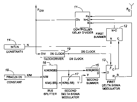
A preferred embodiment of the present invention will now be described with
reference
to Figure 4. The fractional divider shown in Figure 4 comprises a Controlled
Delay Divider
11 which divides a high frequency input signal with frequency Fo to provide an
output signal
with frequency FDIV having its period responsive to a division ratio value,
N+C, supplied
by a first summer 12 and a delay responsive to a Residual Quantization Error
signal, R,
supplied by a first delta-sigma modulator 13. The first summer 12 provides the
division
control value N+C in response to a quantized dithered value C supplied by the
first delta-
sigma modulator 13 and an integer value N input via a port 14. The first Delta-
Sigma
modulator provides the quantized dithered value, C, and the Residual
Quantization Error, R,
in response to a dithered value, D, supplied by a second summer 15. The second
summer
CA 02480258 2004-09-23
WO 03/084069 PCT/CA03/00447
sums a most significant part K/MMSB of a fractional input value provided by a
bus splitter
16 and a noise-shaping quantized value Y supplied by a second Delta-Sigma
modulator 17.
The second delta-sigma modulator 17 quantizes a least significant fractional
value K/MLSB
from the bus splitter 16 to form the noise-shaping quantized value Y. The bus
splitter 16
5 derives the most significant bits K/MMSB and the least significant bits
1{/MLSB by splitting
a fractional value KIM inputted via a second port 18. The first and second
delta-sigma
modulators 13 and 17 are clocked by a Delta-Sigma Clock, DS Clock, from a
clock driver
19. In Figure 4, the clock driver 19 is shown using the output pulse Fdiv to
derive the Delta-
Sigma Clock DS Clock. It is possible, however, to derive the clock signal in
other ways, such
10 as, for example, from a PLL reference clock signal or from within the
Controlled Delay
Divider.
The divider shown in Figure 4 operates as follows:
The high frequency signal is substantially sinusoidal and has a frequency Fo
of 2 GHz.
The Controlled Delay Divider 11 may provide 16 possible delays in increments
of 1/16th of
a cycle of the high frequency input signal Fo. Different binary values of the
Residual
Quantization Error R ranging from 0 to 15 will select corresponding delays
ranging from
1/16th to one cycle of the input frequency Fo.
The division ratio value N+C from first summer 12 is a 7-bit unsigned binary
number
between 64 and 127 which the first summer 12 produces by adding a two's
complement 4-
bit binary number, C, (-4 to +3) to an unsigned 7-bit binary number N (67 to
123). Sign
extension of C may be required. The LSB of Y is added with the same weight as
the LSB
of KiMMSB, i.e., the numbers C and N are added bit by bit beginning with the
LSB of each.
The first Delta-Sigma modulator 13 produces the 4-bit signed value C and the 4-
bit
unsigned value R from an 8-bit signed (two's complement) input D. The first
Delta-Sigma
modulator 13 is a first-order Delta-Sigma modulator with a multi-bit
quantizer. It should be
noted that an accumulator (being equivalent to a first-order Delta-Sigma
modulator with a
single-bit quantizer) is in adequate for some combinations of K/MLSB and Y.
The second summer 15 adds an 8-bit signed binary number Y to a 4-bit unsigned
binary number K/MMSB to produce the 8-bit signed input D. The LSB of Y is
added with
the same weight as the LSB of K/MMSB, as in the case of C and N. Since K/MMSB
is
unsigned, sign extension of 1C/MMSB may not be required.
CA 02480258 2004-09-23
WO 03/084069 PCT/CA03/00447
11
The bus splitter 16 provides the four MSB's of the unsigned 24 bit input K/M
as
KNIMSB and the 20 LSBs of the 24 bit input KIM as an unsigned 20 bit value
K/MLSB.
The second Delta-Sigma modulator 17 randomizes and noise shapes the unsigned
20-bit value
KJMLSB to produce the 8-bit output value Y. The four bits of R and KJMNISB
correspond
to the sixteen possible values of controlled delay in the Controlled Delay
Divider.
The second Delta-Sigma modulator 17 conveniently comprises a MASH Delta-Sigma
modulator of the kind described in "Design and Realization of a Digital Delta-
Sigma
Modulator for Fractional-n Frequency Synthesis" by T.P. Kenny, T.A.D. Riley,
N.M Filiol
and M.A. Copeland, presented in the IEEE Transactions on Vehicular Technology,
March
1999, to which the reader is directed for fiirther details. A fourth-order
MASH type of
Delta-Sigma modulator is described in US5495206, which also describes how to
extend it to
higher orders. Preferably, the second Sigma-Delta modulator 17 is 7th order.
Increasing the order of the second Delta-Sigma modulator 17 improves the
randomization of Residual Quantization Error signal R and thus reduces the
spurs. If higher
order modulators are used, the range of values for Y, D, C and N+C will have
to increase,
possibly requiring wider buses for these signals. Correspondingly, either the
range of N+C
accepted by the Controlled Delay Divider 11 will have to increase or the range
of N will have
to decrease.
The clock driver 19 which supplies the Delta-Sigma Clock (DS Clock) must
provide
drive capability to clock all flip-flops in the two Delta-Sigma modulators 13
and 17 with
clock skew adequate for the timing tolerances of the flip-flops.
In operation, using the randomized Residual Quantization error R shown in
Figure
5(a) as the delay control for the divider 11 causes the Delay Error in the
divider output signal
Fdiv to be randomized also, as shown in Figure 5(b). Consequently, spurs are
reduced, since
the delay error appears randomized rather than periodic.
As shown in more detail in Figure 6, the first Delta-Sigma modulator 13 of
Figure 4
comprises a second bus splitter 20 which provides a predetermined number of
LSBs of a
delayed summed signal X1 as the Residual Quantization Error signal R, and
provides
remaining MSBs of delayed summed signal X1 as the quantized dithered value C.
The
second bus splitter 20 provides 4 LSBs in order to permit selection of 16
possible delays in
the Controlled Delay Divider 11. A delay device 21 derives the delayed summed
signal X1
CA 02480258 2004-09-23
WO 03/084069 PCT/CA03/00447
12
by delaying, by one cycle of the Delta-Sigma Clock DS Clock, a summed signal X
from a
third summer 22. Where the second Delta-Sigma modulator 17 is 7th order, the
delayed
summed signal X1 is an 8- bit signed binary number, and the delay can be
implemented with
eight flip-flops clocked by the Delta-Sigma Clock "DS Clock".
The third summer 22 derives the summed signal X by summing the dithered value
D
from second summer 15 (Figure 4) and the Residual Quantization Error R from
the LSBs
output of second bus splitter 20. Where the second Delta-Sigma modulator 17 is
7th order,
the summed signal X is an 8-bit signed binary number, and can be implemented
with an 8-bit
adder. Since the residual Quantization error signal R is only four bits wide,
some of the
segments of the 8-bit adder can be reduced to half adders rather than full
adders.
The Controlled Delay Divider 11 preferably is a Programmable-Delay Controlled
Delay Divider, as shown in Figure 7, comprising a multiple input single output
(MISO) delay
line 23, a divider unit 24 and a control unit 25 which selectively routes the
output from the
divider 24 to the inputs of the MISO delay line 23. Such a Controlled Delay
Divider 11
advantageously can be used with a VCO producing only one output phase. This
makes it
convenient to have an off-chip VCO or any VCO which does not generate multiple
phases,
such as a VCO based on an LC tank resonator. The Programable-Delay Controlled
Delay
Divider 11 produces a controlled delay on the rising edge of the divided
signal FDIV in
response to the Residual Quantization Error R and a period responsive to the
division control
signal N+C. When the delay is controlled on only the rising (or falling) edge,
the phase
detector used in any PLL synthesizer should be rising (or falling) edge
triggered.
The MISO delay line 23 has multiple inputs and one output with the output
being
related to one of the inputs so that, when the active input is held high, the
output will also
eventually be high (or alternatively low) and when the active input is held
low, the output will
eventually be low (or alternatively high). There is a different delay for each
path through the
MISO delay line, though the logical output of the MISO delay line does not
depend on the
propagation path from input to output.
The MISO delay line 23 provides a delay which depends upon the input used as
the
active input. This is accomplished by having multiple stages in the delay
line, with one input
for each stage, with each stage contributing some delay. The stages near the
end of the delay
line then will have less delay and the stages near the beginning of the delay
line will have more
CA 02480258 2004-09-23
WO 03/084069 PCT/CA03/00447
13
delay. Thus, referring again to Figure 7, the stages of the MISO delay line 23
comprise
logical OR gates 261,..., 26n, each of which has a first input connected to
the output of the
previous gate and a second input coupled to the control unit 25 to receive a
respective one
of a plurality of delay control signals xbl,
xbn. Because the OR gates 261,..., 26n are
connected in series, the delay control signal xbn will pass through only one
OR gate 26n
producing a delay of TO/n, while the delay control signal xbn-1 will pass
through two OR
gates 26n-1 and 26n producing a delay of 2To/n, and so on. A delay control
signal xbl will
pass through all of the OR gates 261,..., 26n producing a delay of TO. Thus,
as an example,
if the MISO delay line 23 has 16 inputs xbl to xb16 and 16 OR gates 261,...,
2616, each
stage will provide a delay dT = To/16 ¨ 1/16F0.
The control unit 25 controls the delay through the MISO 23 by selecting the
appropriate one of the MISO delay control signals xbl, xb2, xbn
for application to the
corresponding stage of the MISO delay line 23. As shown in Figure 7, the
control unit 25
comprises a set of AND gates 271,..., 27n each having one input coupled to the
output of the
divider unit 24 and the other input to a logic unit 28 which enables the AND
gates 271,...,
27n selectively in dependence upon the Residual Quantization Error R. The
outputs of the
AND gates 271,..., 27n are coupled to the second inputs of the logical-OR
gates 261,..., 26n,
respectively.
The logic unit 28 provides the ENABLE signals for the AND gates in response to
the
Residual Quantization Error signal R. Preferred encoding for R is a binary
code because this
simplifies the first Delta-Sigma modulator 13 (Figure 6). The logic unit 28
decodes binary
code for R to provide the signals xal, xa2 xan-1, xan so that, when R calls
for minimum
delay, the propagation of the output signal P1 from divider unit 24 to the
delay line goes
through AND gate 27n and, when R calls for a maximum delay, the propagation of
output
signal P1 to the delay line goes through AND gate 271. For example, if R is a
binary encoded
4-bit number, the logic unit 28 would decode xan for R=0, xa2 for R=14, xal
for R=15, and
so on. The logic unit 28 may not be necessary if, for example, R is directly
thermometer
coded rather than binary coded.
The divider 24 comprises a 7-bit loadable down counter 29 and a first decoder
30 for
determining when the counter 29 is within the last 16 cycles of its count. The
down-counter
29 counts down when in a non-zero state and loads a new value, N+C, when in
the zero state.
CA 02480258 2004-09-23
WO 03/084069 PCT/CA03/00447
14
On each rising edge of the high frequency signal with frequency Fo, the
counter 29 advances
to the next state.
The decoder 30 provides a timing signal Si which is a logical 1 output when
the state
of the counter 29 is less than or equal to some predetermined state and a
logical 0 otherwise.
The signal S I could serve directly as the output of divider 24 but it is
preferred to use
flip-flop 31 to retimes the Si signal. This reduces timing errors introduced
by the decode unit
30. Thus, the output of the decoder 30 advantageously is re-synchronized to
the high
frequency input signal FO. This re-synchronization reduces the effect of power
supply
dependent delays in the counter 29 and the decoder 30. The re-synchronization
is provided
by means of a flip-flop 31 clocked by the high frequency signal FO. The output
of the
decoder 30 is supplied to data input D of the flip-flop 31 and the output of
the flip-flop 31
provides the output pulse P1 of the divider 24.
The logic block 28 may comprise a series of binary decoders arranged to decode
a
binary input of R=0 to set only xan to a logic one, thus enabling a path from
P1 through xbn
to produce a minimum delay. Similarly, the binary decoders would decode R = ¨I
to set only
xa 1 high enabling a path through xbl for a maximum delay. For intermediate
delays, the
binary decoders would decode the corresponding value of R to select the
appropriate one of
the intermediate OR gates 262,..., 26n-1.
Enabling only one of the AND gates 271,..., 27n enables only one path for the
output
signal P1 through to the FDiv output of the Controlled Delay Divider 11. (With
the OR gate
based delay line, enabling only xa3, for example, is equivalent to enabling
xa3 and any
combination of xal or xa2; enabling only xa3 is more instructive.)
For an ideal MISO delay line 23 with n stages, the delay of each stage is
equal. For
an ideal MISO delay line as used in a Programable-Delay Controlled Delay
Divider, the
difference in delay from the minimum to the maximum should be exactly (n-1 )/n
times one
period of the high frequency signal with frequency, Fo. Practical delay lines,
however, will
have unequal delays due to mismatches in the delay stages. Process variation
may also result
in all of the delays being slower or faster. The deviations from ideal
behaviour result in
spurious output frequencies from the synthesizer but are mitigated by the
pseudo-randomization of the second Delta-Sigma quantizer. This may require
"binning" or
selecting the devices following manufacture for use at particular frequencies
depending on
CA 02480258 2004-09-23
WO 03/084069 PCT/CA03/00447
the process variations; or may require good process control to get the
variations within
acceptable limits.
In order to obtain the lowest level of spurs, every effort should be made to
make sure
that the delay of each stage matches and that the difference in delay from the
minimum to the
5 maximum delay is close enough to ideal for the prescribed operating
frequency FO.
It may also be necessary to control the ambient temperature about the delay
line to
remove temperature variations or to use temperature or voltage to control the
delay. The
voltage or temperature used to control the delays can be controlled with a
feedback loop.
Figure 8 is an illustration in block diagram form of a Programable-Delay
Controlled
10 Delay Divider 11' similar to that of Figure 7 but with two
modifications, one to address the
problem of delay variations and the other to provide a delayed output pulse.
The
Programmable-Delay Controlled Delay Divider 11' comprises a controllable-delay
MISO
delay line 23', a control unit 25, and a divider unit 24. The control unit 25
and divider unit
24 are identical to those shown in Figure 7. The MISO delay line 23', however,
differs in
15 that all of the delays can be reduced or increased by means of a control
signal Vc.
In normal operation, the Programmable-Delay Controlled Delay Divider II '
operates
in the same manner as that described with reference to Figure 7. Periodically,
however, the
Programmable-Delay Controlled Delay Divider 11' performs a calibration cycle
to determine
changes in the delay provided by the MISO delay line 23' and makes appropriate
adjustments
to the delays 26'1,..., 26'n to compensate. The calibration circuitry
comprises a second
decoder 32, second and third flip-flops 33 and 34, three additional AND gates
35, 36 and 37,
a phase detector 38, and a NOT inverter 39, operation of which will now be
described.
As before, the counter 29 loads an initial value I and counts down with the
value of
the Count reduced by one for each cycle of the high frequency signal with
frequency Fo. The
value of the Count starts at the initial value I, determined by N+C, and is
reduced through
states!, I-1 ..., S2+2, S2+1, S2, .... Sl, and finally 0, whereupon the
counter 29 loads a new
value of!, determined by N+C again, and continues. The Count which represents
the counter
state (or some of its MSBs) is provided to first decoder block 30, as before,
and to the
second decoder block 32. The second decoder block 32 produces a second timing
signal S2,
which is high when the Count is equal to some predetermined state higher than
that which
CA 02480258 2004-09-23
WO 03/084069 PCT/CA03/00447
16
corresponded to Si as described above. As before, the first decoder block 30
produces a
timing signal S1 which is high when the divider is in state SI or lower.
The second retiming flip-flop 33 retimes the timing signal S2, producing a
delay line
input pulse P2 which is applied to the input of the MISO delay line 23'. The
third flip-flop
34 delays the pulse P2 from second flip-flop 33 by one cycle of the high
frequency signal with
frequency Fo, producing a calibration pulse P3 which is supplied to one input
of AND gate
36. The second and third flip-flops 33 and 34 are clocked by the high
frequency input signal
FO.
The output of the MISO delay line is supplied to one input of the other AND
gate 35.
The outputs of the AND gates 35 and 36 are applied to respective inputs of the
phase
detector 38. The other inputs of the two AND gates 35 and 36 are connected in
common to
the output of NOT inverter 39, the input of which is coupled to the output of
first retiming
flip-flop 31. The output of the phase detector is the control signal VC which
is supplied to
the MISO 23' and used to adjust the delays therein. The output of the MISO
delay line 23'
and the output of the first retiming flip-flop 31 are supplied to respective
inputs of AND gate
37, whose output is the output signal FDIV.
In this embodiment, a calibration is performed before each output pulse is
generated.
Following output of a previous pulse, the NOT inverter 39 enables the AND
gates 35 and 36
to pass the output of the delay line 23' and output of third retiming flip-
flop 34 to be applied
to the phase detector 38, which detects whether or not the output of the delay
line 23' arrives
before or after the output of the third retiming flip-flop 34 and adjusts each
of the delay
stages by the same amount so as to reduce any difference.
On the next cycle, the NOT inverter 39 will disable the AND gates 35 and 36 so
that
the next pulse from the MISO delay line 23' will be supplied via AND gate 37
as the output
pulse FDIV.
The feedback provided by the phase detector 38 is negative feedback resulting
in a
stable Delay locked loop. For example, if the output of the delay line 23'
arrives earlier than
the calibration pulse, the delays should be increased. Conversely, if the
output of the delay
line 23' arrives later than the calibration pulse, the delays should be
decreased.
As mentioned earlier, the second modification is to provide a delayed output
pulse.
Thus, a third decoder 40 has its input connected to the output of counter 29
and responds to
CA 02480258 2004-09-23
WO 03/084069 PCT/CA03/00447
17
the state of the counter 29 to provide a third timing signal, SO, when the
Count is in state 0.
Because this occurs after state SI, as the counter 29 counts down, the output
(SO) of the
decoder 40 can be provided as the signal DO, i.e., as an extra output from the
Programmable-Delay Controlled Delay Divider 11'. As shown in Figure 9, which
is similar
to Figure 4, this second divider output DO may be used by Delta-Sigma Clock
source 19'
(Figure 4) to generate the DS Clock used to clock the digital logic i.e., the
first Delta-sigma
modulator 13 and second Delta-sigma modulator 17 (Figure 4) at a time slightly
delayed from
the edge that triggers the phase detector 38. This reduces interference from
the digital logic
to the phase detector 38.
Figure 10 is an illustration in block diagram form of the fractional divider
of Figure
9 incorporated into a PLL to form a frequency synthesizer. In this case, the
Delta-Sigma
Clock signal DS Clock is derived from the second divider output DO, though it
could be
derived in the manner shown in Figure 4. Use of the fractional divider in a
phase locked loop
allows the high frequency signal, with frequency FO to be the synthesizer
output, which is
useful when the invention is used as part of a local oscillator in a radio.
The PLL comprises
a phase frequency detector (PFD) 41, a charge pump 42, a loop filter 43 and a
VCO 44. A
signal of frequency FREF from a reference source 45 is applied to the
reference input of the
phase frequency detector 41 and the signal FDIV from the fractional divider is
applied to the
other DIVIDER input of the phase frequency detector 41. The UP and DOWN
outputs of
the PFD 41 are applied to the charge pump 42 to control its output current ICP
which loop
filter 43 converts to a corresponding control voltage VCP which adjusts the
frequency of the
VCO 44, providing the high frequency signal FO which is both the output of the
frequency
synthesizer and the input to the fractional divider.
The PLL also provides filtering to remove the noise-shaped quantization error
introduced by the second Delta-Sigma modulator.
In embodiments of any of the various aspects of the invention arbitrarily fine
resolution may be obtained by increasing the resolution (number of bits) of
the second DSM.
The invention also comprehends an adjustable delay line per se having means
for
calibrating average element delay by comparing the total actual delay provided
by the delay
line with a reference period equal to the prescribed total delay.
CA 02480258 2004-09-23
WO 03/084069 PCT/CA03/00447
18
INDUSTRIAL APPLICABILITY
Embodiments of the invention advantageously may be used in frequency
synthesizers,
especially those that are part of a larger integrated circuit with on-chip or
off-chip resonator-
based oscillators.
An advantage of the Programmable-Delay Controlled Delay Divider in which the
delay line is calibrated is that it can widen the range of frequencies (FO)
over which the delays
are correct for a given chip sample and temperature. It can also be used to
correct for a wider
range of temperature or for process variation.
Advantageously, in embodiments of the present invention the step size of the
quantization noise, as compared to known Delta-Sigma synthesizers and the
effect of
Controlled Delay Divider delay nonlinearity is reduced as compared to known
Controlled
Delay Divider based dividers. Moreover, embodiments of the invention reduce
the level of
spurs by randomizing the controlled delays and thereby randomizing the Delay
Error.