Note: Descriptions are shown in the official language in which they were submitted.
' ' ~ ' CA 02480691 2004-09-27
Schott Glas
0 3 SGLfl 13 b~A~~
Process for forming a housing for electronic modules, and
electronic modules hermetically encapsulated in this way
Description
The invention relates to a process for forming housings for
electronic modules, and to electronic modules that are
hermetically encapsulated in this way, in particular sensors,
io integrated circuits and optoelectronic components.
To encapsulate integrated circuits and optoelectronic
components, it is known to use an organic adhesive layer to
bond a thin plate of glass onto the module and thereby to
i5 cover and protect the sensitive semiconductor structures.
This design has the drawback that over the course of time
water can diffuse into the organic adhesive layer and can
then reach and damage the semiconductor structures.
Furthermore, the adhesive layers may age as a result of UV
2o irradiation, which is damaging in particular to
electro-optical modules.
As an alternative to organic adhesives, low-melting glass
solder has also already been used as an intermediate layer
2s which has been sprayed on, sputtered on or applied by means
of screen-printing and dispenser technology. The process
temperature for melting the glass-solder layer, however, is
higher than T=300°C, which means that temperature-sensitive
semiconductor structures cannot be encapsulated.
CA 02480691 2004-09-27
2
The invention is therefore based on the object of providing a
process for encapsulating electronic modules which makes it
possible to achieve encapsulation which is substantially
resistant to water diffusion yet is carried out at moderate
temperatures below 300°C, preferably below 150°C.
The object set is achieved on the basis of the measures
described in claim 1 and is configured and developed further
to by the further measures of the dependent claims. Claim 24
relates to an electronic module producible in accordance with
the invention, with advantageous refinements and
configurations being given in the claims that are dependent
on claim 24.
One advantage of coating with a vapor-deposition glass is the
application of the insulating glass layer at room temperature
up to approximately 150°C, so that there is no likelihood of
damage or oxidation of the substrate surface whatsoever, even
with metal substrates. In this context, reference is also
made to the following applications:
DE 202 05 830.1, filed on 04.15.2fl02,
DE 102 22 964.3, filed on 05.23.2002;
DE 102 22 609.1, filed on 05.23.2002;
DE 102 22 958.9, filed on D5.23.2002;
DE 102 52 787.3, filed on 11.13.2002;
DE 103 O1 559.0, filed on 01.16.2003;
in the name of the same Applicant, the content of disclosure
of which is hereby expressly incorporated by reference.
With regard to the barrier properties of vapor-deposition
glass layers, measurements have shown that with layer
thicknesses of the vapor-deposition glass layer in the range
' ~ ' CA 02480691 2004-09-27
3
from 8 ~tm to 18 Vim, helium leak rates of less than
10-7 mbar 1 s-1 or less than 10-a mbar 1 s-1 are reliably
achieved. The measurements, for layers with a thickness of 8
~m and 18 ~m have even revealed helium leak rates of between
0 and 2 x 10⁻⁹ mbar 1 s-1, and even these upper limit values
are significantly influenced by the measurement inaccuracy of
the tests carried out.
The process according to the invention for encapsulation with
io vapor-deposition glass can even be employed if the electronic
module is attacked while it is still being produced.
The thickening of the substrate of the electronic module
produced by the vapor-deposited glass layer is utilized to
i5 stabilize the substrate while actions are being carried out
on the substrate from the unencapsulated side. The otherwise
finished electronic module may also be encapsulated from the
connection side, leaving clear the connections themselves.
For this purpose, the substrate may, for example, be provided
2o with a passivation layer on the opposite side from a first
side having the semiconductor structures. By way of example,
a plastic layer is suitable for this purpose. The passivation
layer may also comprise a glass layer which is preferably
vapor-deposited onto this side.
The process is particularly suitable for packaging components
which still form part of a wafer (wafer level packaging), in
which case the substrate comprises a wafer having the
substrates of the components, which can be separated from the
3o wafer after they have been packaged.
Depending on the particular requirements, the thickness of
the vapor-deposited glass layer may be from 0.01 to 1000 Vim.
' ' ' CA 02480691 2004-09-27
4
If it is merely a matter of hermetically sealing the
module to be protected, it is preferable for the glass layer
thickness to be in the range between 0.1 and 50 Eun. If the
loads imposed are greater, the glass layer thickness is
s increased accordingly, with a preferred range for the glass
layer thickness being between 50 and 200 Vim. It is also
possible to build up multiple layers in combination with
other materials. It is, furthermore, possible for the glass
layer to be combined with an applied plastic layer in order
to to structurally reinforce the electronic module.
There are various options for the vapor deposition of glass.
It is preferable to generate the glass vapor from a stock
glass target by means of electron beam. It is possible to
15 generate vapor-deposition rates of more than 4 ~,m/min, and
the glass produced is deposited with a secure bond on the
surface of the substrate without needing an increased H20
content for a bonding action, as is the case with low-melting
glass solder. The preferred vapor-deposition glass is a
2o borosilicate glass containing aluminum oxide and alkali metal
oxide fractions, such as for example the vapor-deposition
glass of type 8329 produced by Schott Glas. Moreover, this
glass has a coefficient of thermal expansion which is close
to that of the substrate for standard semiconductor
2s structures or can be matched to the coefficient of thermal
expansion of the substrate by suitable modification to the
components. It is possible to use vapor-deposition glass of
other compositions, in particular in a plurality of layers on
top of one another, in which case the glasses of the layers
3o may have different properties with regard to refractive
index, density, hardness, etc.
' ' ' ' CA 02480691 2004-09-27
The vapor-coating of the substrate with a glass layer
may advantageously also encompass plasma ion assisted
deposition (PIAD). In this case, an ion beam is additionally
directed onto the substrate to be coated. The ion beam may be
5 produced by way of a plasma source, for example by ionization
of a suitable gas. The plasma results in additional
densification of the layer and the removal of loosely
adhering particles from the substrate surface. This leads to
particularly dense, low-defect deposited layers.
to
Furthermore, by selecting a suitable combination of
materials, it is possible to realize the application of a
mixed layer of inorganic and organic constituents. This mixed
layer is characterized by a reduction in its brittleness.
If the glass layer is applied to a first side of the
substrate of the electronic module before this electronic
module has been fully produced, it may be expedient, for
handling purposes during completion of production, to apply a
2o plastic layer, which reinforces the module, above the glass
layer. In this case, the glass layer is produced with a
thickness which is sufficient for encapsulation or hermetic
seal with respect to the penetration of diffusing substances,
while the plastic layer is produced in a thickness which is
required for stabilization during further processing of the
module.
In such a case, it is possible for material to be removed
from the second, unencapsulated substrate side, so that it is
so possible to produce connections to the module which extend
into the module from the underside and are therefore
protected by the module itself when the module is finally
installed at its position of use. This is of significance in
' ~ ' CA 02480691 2004-09-27
6
particular in the case of sensors.
The invention is described with reference to the drawing, in
which:
s
Fig. 1 shows a section through a wafer with a
vapor-deposited glass layer,
Fig. 2 shows a wafer section with glass and plastic
layer,
io Fig. 3 shows the production of connections to the
wafer,
Fig. 4 shows the additional plastic passivation of
the wafer underside,
Fig. 5 shows the coating of the wafer underside with
is vapor-deposition glass,
Fig. 6 shows the application of a ball grid array to
the wafer shown in Fig. 5,
Fig. 7 shows a further way of applying the ball grid
array,
2o Fig. 8 shows the encapsulation of the underside of a
wafer,
Fig. 9 shows the application of the ball grid arrays
to the wafer shown in Fig. 8,
Fig. 10 shows a diagram illustrating a vaporization
2s arrangement,
Fig. 11 shows results of a TOF-SIMS measurement, and
Fig. 12 shows an electron microscope transverse
microsection image.
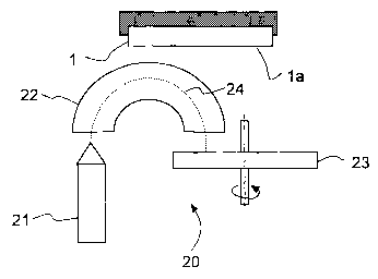
3o Fig. 10 shows the arrangement of a substrate 1 with respect
to a vapor-deposition glass source 20 which comprises an
electron beam generator 21, a beam-diverter device 22 and a
glass target 23 on which the electron beam 24 impinges. ~t
' ' ' CA 02480691 2004-09-27
7
the location at which the electron beam impinges, the
glass is vaporized and is then deposited on the first side 1a
of the substrate 1. To allow the glass from the target 23 to
be vaporized as uniformly as possible, the target is rotated
s and the beam 24 sweeps back and forth along it. In addition,
the arrangement may also comprise a plasma source for
generating an ion beam which, in operation, is directed onto
the side la that is to be coated, in order for the substrate
to be coated with a glass layer by means of plasma ion
to assisted deposition (PIAD).
For more details concerning the possible substrate 1,
reference is made to Fig. 1. A silicon wafer as the substrate
1 includes regions 2 having semiconductor structures and
is regions 3 having connection structures, for example made from
aluminum. The connection structures may, for example,
comprise bond pads or other connection surfaces. The silicon
wafer constitutes a substrate with a surface roughness of
< 5 Vim. The top side 1a of the substrate is on the opposite
2o side from the underside 1b. A glass layer 4, which has
preferably been obtained from the vapor-deposition glass of
type 8329 produced by Schott, has been deposited on the top
side la. This type of glass can be substantially vaporized by
the action of the electron beam 24, the work being carried
2s out in an evacuated environment at 10-9 mbar residual
pressure and a bias temperature during the vaporization of
100°C. Under these conditions, a dense, continuous glass
layer 4 is produced, and this layer is substantially
impermeable to gases and liquids, including water, but
3o transmits light, which is important in the case of
electro-optical modules.
The glass layer 4 may also include a plurality of individual
' ' ' ' CA 02480691 2004-09-27
8
layers, for example made from glasses with different
compositions. The glass layer may also comprise a mixed layer
formed from inorganic and organic constituents in order, for
example, to achieve an increased layer flexibility.
The underside 1b of the wafer is available for further
processing steps, which include wet, dry and plasma etching
or cleaning.
io If, as in Fig. 1 and the further Figs. 2 to 9, the substrate
used is a wafer, the process according to the invention may
expediently be used to package components which still form
part of a wafer. However, the process can also be applied in
a similar way to chips which have already been separated from
is the wafer and comprise semiconductor structures and
connection structures.
Fig. 2 shows a covering layer for the substrate l, comprising
a glass layer 4 and a plastic layer 5. The glass layer 4 has
2o a thickness in the range from 1 to 50 Vim, which is sufficient
for the encapsulation or hermetic sealing, while the plastic
layer 5 is thicker, in order to impart greater stability to
the wafer as a workpiece for subsequent treatment steps.
2s Fig. 3 shows the further treatment of a wafer. The wafer is
thinned on the underside, so that the components that can be
produced in accordance with the invention have a thinned
substrate, and etching pits 6 are produced, extending as far
as the connection structures 3, which act as an etching stop.
3o The wafer underside 1b is provided with a plastic lithograph,
with the regions of the connection structures 3 remaining
open. Then, line contacts 7 are produced on the underside,
for example by spraying or sputtering, with the result that
' ' CA 02480691 2004-09-27
9
conductive layers 7 are produced in the region of the
etching pits 6. Then, the plastic used for the lithography is
removed from the wafer underside 1b. Next, a ball grid array
8 is applied to the conductive layers 7, and the wafer is
divided along planes 9. The result is a plurality of
electronic modules whose semiconductor structures 2 are
safely embedded between the covering layer 4 and the
substrate 1 such that they are hermetically sealed.
to Fig. 4 shows a modification to the embodiment shown in Fig.
3. The same process steps as those described above are
carried out, but the plastic on the wafer underside lb is not
removed and covers the underside as a passivation and
protective layer 10.
Fig. 5 shows an embodiment in which a vapor-deposited glass
layer 11 is to be applied to the underside lb of the
substrate instead of the plastic layer 10. As in the
embodiment shown in Fig. 3, the plastic used for lithography
2o is removed from the wafer underside lb, and the entire
underside 1b of the wafer is vapor-coated with the glass,
producing a 1 to 50 Nm thick glass layer 11.
The glass layer 11 shown in Fig. 5, like the plastic layer 10
illustrated in Fig. 4, serves as a protective or passivation
layer.
As illustrated at llb, this glass layer also covers the
outwardly projecting parts of the line contacts 7. To apply a
3o ball grid array 8, these regions llb are uncovered by being
ground and/or etched away. Then, the ball grid arrays are
applied, as shown in Fig. 6, and the wafer is then divided up
in order to form individual modules, and indicated at 9. The
' ' ' CA 02480691 2004-09-27
1~
sensitive semiconductor structures 2 are protected at
the top and the bottom by a respective glass layer 4 and 11.
In a further embodiment of the invention, the wafer is
s divided up at parting planes 9 which do not pass through the
connection structures. This has the advantage that it is also
possible to ensure a lateral passivation protection for the
modules. Fig. 7 shows an example of dividing up the wafer
which only affects material of the covering layer 4 and of
to the substrate 1. The procedure is initially the same as for
the exemplary embodiments described above, i.e. the wafer is
thinned from the underside and etching pits 6 which extend as
far as the underside of the connection structures 3 are
produced. The wafer underside 1b is lithographed, with the
i5 regions of the connection structures remaining open. The line
contacts 7 are produced in the region of the etching pits 6,
with the etching pits also being filled with conductive
material 12. In this context, thickening by electroplating
using Ni(P) may be considered. The components producible in
2o accordance with this embodiment of the invention accordingly
have through-contacts passing through the substrate.
After the plastic has been removed from the wafer underside
at least in the region of the contacts 7, the ball grid
2s arrays 8 are applied. This is followed by dividing up the
wafer along planes 9. The result is electronic modules with
hermetically sealed semiconductor structures 2, with an
analogous plastic layer 10 being present or absent depending
on the procedure employed.
Figs. 8 and 9 show an exemplary embodiment involving the
production of a glass layer 11 on the underside. The
procedure is similar to that of the embodiment shown in Fig.
' ' ' CA 02480691 2004-09-27
11
in conjunction with Fig. 7, i.e. filled regions are
produced beneath the connection structures, and the entire
underside lb of the wafer is coated with the glass layer 11,
which is then removed in the region of the filled etching
5 pits 6 in order for the ball grid arrays to be applied
thereto, as shown in Fig. 9. After the wafer has been divided
up along planes 9, modules with encapsulated semiconductor
structures 2 are obtained.
1o The glass system of the layer 4 or 11 should form at least a
binary system. Multicomponent systems are preferred.
Vapor-deposition glass which has the following composition,
in percent by weight, has proven particularly suitable:
Components % by weight
Si02 75 - 85
B203 10 - 15
Na20 1 - 5
2o Li20 0.1 - 1
K20 0 . 1 - 1
A1203 1 - 5
A preferred vapor-deposition glass of this type is glass $329
produced by Schott, having the following composition:
Si02 84 . 1 %
B203 11 . 0 %
3o Na20 ~ 2 . 0 % ]
K20 ~ 0.3%} 2.3% (in the layer ? 3.3%)
Li20 ~ 0 . 3 % ]
' ' ' ' CA 02480691 2004-09-27
12
A1203 ~ 2.60 (in the layer < 0.5%)
The values given in parentheses represent the proportions by
s weight of the respective component in the vapor-deposited
layer.
The electrical resistance is approximately 101° S2/cm (at
100°C),
to the refractive index is approximately 1.470,
the dielectric constant s is approximately 4.7 (at 25°C, 1
MHz), and tg8 is approximately 45 x 10-4 (at 25°C, 1 MHz).
A further group of suitable vapor-deposition glasses has the
15 following composition, in percent by weight:
Components: % by weight
Si02 65 - 75
B203 20 - 30
2o Na20 0.1 - 1
Li20 0.1 - 1
K20 0 . 5 - 5
A1203 0.5 - 5
2s A preferred vapor-deposition glass from this group is 'the
glass 6018-189 produced by Schott having the following
composition:
Components: % by weight
3o Si02 71
B203 2 6
NazO 0 . 5
' CA 02480691 2004-09-27
13
Li20 0 . 5
K20 1.0
A1203 1 . 0
s The glasses 8329 and 6018-189 that are preferably used in
particular have the properties as listed in the table below:
Properties 8329 6018-189
a2o-soo [ 10 6K 1 ] 2 . 7 5 3 . 2
Density (g/cm') 2.201 2.12
Transformation point [C] 562 742
Refractive index nd 1.469 1.465
Hydrolytic resistance class 1 2
according to ISO 719
Acid resistance class according 1 2
to DIN 12 116
Alkali resistance class 2 3
according to DIN 52322
Dielectric constant s (25C) 4.7 3.9
(lMHz) (40GHz)
tan8 (25C) 45*10-'' 26*10-''
(lMHz) (4flGHz)
To produce particular properties in the modules, it may be
io expedient to use glasses of different compositions for the
glass layers on the top side and on the underside. It is also
possible for a plurality of glasses having different
properties, e.g. with regard to refractive index, density, E
modulus, Knoop hardness, dielectric constant, tank to ,be
i5 deposited successively on the substrate.
As an alternative to electron beam deposition, it is also
' ' ' CA 02480691 2004-09-27
14
possible to use other means for transferring materials
which are deposited in glass form. For example, the
vapor-coating material may be in a crucible which is heated
by electron impact heating. Electron impact heating of this
s type is based on thermionic discharges which are accelerated
onto the crucible in order to impact on the material to be
vaporized with a predetermined kinetic energy. These
processes likewise make it possible to produce glass layers
without excessive thermal loading on the substrate on which
to the glass is deposited.
The following text present results of various tests carried
out on vapor-deposited glass layers formed from glass 8329.
15 Fig. 11 shows the results of a TOF-SIMS measurement, in which
the count rate is plotted as a function of the sputtering
time. The measurement characterizes the profile of the
element concentrations in the direction perpendicular to the
substrate surface. A thickness constancy for the glass frame
20 of < 1% of the layer thickness was determined.
Fig. 12 shows an electron microscope transverse microsection
image of a silicon substrate coated with the vapor-deposition
glass 8329. The vapor-deposition glass and the surface of the
2s silicon substrate are securely bonded to one another in a
manner which is not released even by the transverse
microsectioning operation involved in preparing the specimen.
Furthermore, resistance and stability measurements were
3o carried out on a vapor-deposition glass layer formed from
vapor-deposited glass 8329, in accordance with DIN/iSO. The
results are given in Table 1.
CA 02480691 2004-09-27
Table 1:
Specimen designation:
8329
I
Water DIN ISO
Consumption NazO
Comment
719 of equivalent
s
Class HC1 [ml/g]
[~g/g]
HGB 1 0.011 3 none
Acid DIN 12116 Material Total Comment
Class removal surface area s/visib
[ mg / dm2 ] [ cm2 ] 1 a
.changes
1 W 0.4 2 x 40 unchang
as material ed
Alkali DIN ISO Material Total Comment
695 removal surface area s/visib
Class [mg/dm2] [cmz] le
changes
A 2 122 2 x 14 unchang
As material ed