Note: Descriptions are shown in the official language in which they were submitted.
CA 02480992 2004-09-09
RADIATION DETECTOR
BACKGROUND OF THE INVENTION
(1) Field of the Invention
This invention relates to radiation detectors of the
direct conversion type including a radiation sensitive
semiconductor for generating electric charges upon incidence
of radiation, for use in the medical, industrial, nuclear and
other fields.
l0 (2) Description of the Related Art
An indirect conversion type radiation detector first
converts radiation (e.g. X rays) into light, and then converts
the light into electric signals by photoelectric conversion.
As distinct from the indirect conversion type, a direct conver-
sion type radiation detector converts incident radiation (e.g.
X rays) directly into electric signals by a radiation sensitive
semiconductor.
As shown in Fig. l, a direct conversion type radiation
detector includes an active matrix substrate 51, a radiation
sensitive semiconductor 52 and a common electrode 53 for
bias voltage application. A lead wire 54 for supplying a bias
voltage is connected to the surface of the common electrode
53. Numerous collecting electrodes (not shown) are formed
on the surface of the active matrix substrate 51, in a
two-dimensional matrix arrangement set within a radiation
-1-
CA 02480992 2004-09-09
detection effective area SA. An electric circuit (not shown)
is arranged on the surface of the active matrix substrate 51
for storing and reading electric charges collected by the
respective collecting electrodes upon incidence of radiation.
The radiation sensitive semiconductor 52 is laid on the
surface of the active matrix substrate 51 where the collecting
electrodes are formed, to generate charges upon incidence of
the radiation. The common electrode 53 for bias voltage
application is formed two-dimensionally on the front surface
l0 of the radiation sensitive semiconductor 52.
In time of radiation detection by the direct conver-
sion type radiation detector, a bias voltage from a bias volt-
age source is applied to the common electrode 53 for bias
voltage application via the lead wire 54 for bias voltage sup-
ply. With the bias voltage applied, electric charges are
generated by the radiation sensitive semiconductor 52 upon
incidence of the radiation. The electric charges generated
by the semiconductor 52 are collected by the collecting elec-
trodes. The electric charges collected by the collecting elec-
trodes are fetched as radiation detection signals from the
respective collecting electrodes by the storage and reading
electric circuit including capacitors, switching elements and
electric wires.
That is, in the direct conversion type radiation detec-
tor, each of the collecting electrodes in the two-dimensional
-2-
CA 02480992 2004-09-09
matrix arrangement acts as an electrode corresponding to
each pixel in a radiographic image (pixel electrode). Radia-
tion detection signals obtained can be used to create a radio-
graphic image according to a two-dimensional intensity
distribution of the radiation projected to the radiation detec-
tion effective area SA.
However, the conventional radiation detector has a
problem that performance lowers as a result of the lead wire
54 for bias voltage supply being connected to the common
l0 electrode 53 for bias voltage application.
Since a hard metal wire such as copper wire is used
for the Iead wire 54 for bias voltage supply, when the lead
wire 54 is connected to the common electrode 53, damage is
done to the radiation sensitive semiconductor 52, leading to
a lowering of performance such as a voltage resisting defect.
Particularly where the semiconductor 52 is amorphous sele-
nium or a non-selenic polycrystalline semiconductor such as
CdTe, CdZnTe, PbI2, HgI2 or TlBr, the radiation sensitive
semiconductor 52 of large area and thickness may easily be
2o formed by vacuum deposition, but such amorphous selenium
and non-selenic polycrystalline semiconductor are relatively
soft and vulnerable to scratch. Even where a carrier selec-
tive intermediate layer that demonstrates a dark current
reducing effect is disposed between the radiation sensitive
semiconductor 52 and common electrode 53, the carrier
-3-
CA 02480992 2004-09-09
selective intermediate layer is far thinner than the
semiconductor 52, and therefore a lowering of performance
such as a voltage resisting defect will occur with the carrier
selective intermediate layer and semiconductor 52 when the
lead wire 54 is connected to the common electrode 53.
SUMMARY OF THE INVENTION
This invention has been made having regard to the
state of the art noted above, and its object is to provide a
radiation detector that can avoid a lowering of performance
resulting from a lead wire for bias voltage supply being con-
nected to a common electrode for applying a bias voltage to a
radiation sensitive semiconductor.
The above object is fulfilled, according to this inven-
tion, by a radiation detector having a radiation sensitive
semiconductor for generating electric charges upon incidence
of radiation, and a common electrode for bias voltage
application formed two-dimensionally on a front surface of
the radiation sensitive semiconductor, a lead wire for bias
voltage supply being connected to a surface of the common
electrode, the detector comprising:
an electrically insulating buffer seat disposed on the
front surface of the radiation sensitive semiconductor, in a
position outside a radiation detection effective area;
the common electrode for bias voltage application
-4-
CA 02480992 2004-09-09
covering at least a portion of the buffer seat;
wherein the lead wire for bias voltage supply is con-
nected to a surface portion of the common electrode located
on the buffer seat.
When the radiation detector acco~cding to this inven-
tion detects radiation, a bias voltage is applied to the com-
mon electrode via the lead wire for bias voltage supply.
With the bias voltage applied, the radiation sensitive
semiconductor, upon incidence of the radiation to be detected,
generates electric charges as sources of radiation detection
signals.
The radiation detector of this invention includes an
electrically insulating buffer seat disposed on the front
surface of the radiation sensitive semiconductor, in a posi-
tion outside a radiation detection effective area. The com-
mon electrode for bias voltage application covers at least a
portion of the buffer seat. The lead wire for bias voltage
supply is connected to a surface portion of the common elec-
trode located on the buffer seat. The buffer seat reduces a
2o shock occurring when the lead wire is connected to the com-
mon electrode. As a result, the radiation sensitive
semiconductor is protected from damage which would lead to
a voltage resisting defect.
The buffer seat for preventing damage to the radia-
tion sensitive semiconductor is disposed outside the radia-
-5-
CA 02480992 2004-09-09
tion detection effective area. Thus, the buffer seat is
provided without impairing the radiation detecting function.
In one specific example according to this invention,
the radiation detector further comprises an active matrix
substrate, the active matrix substrate including:
a plurality of collecting electrodes formed on a
surface of the active matrix substrate, in a one-dimensional
or two-dimensional arrangement set within the radiation
detection effective area; and
l0 an electric circuit arranged on the active matrix sub-
strate for storing and reading electric charges collected by
the respective collecting electrodes are;
the radiation sensitive semiconductor being stacked
on the surface, where the collecting electrodes are formed, of
the active matrix substrate.
In this case, the electric charges generated in the
radiation sensitive semiconductor upon incidence of the
radiation are collected by the respective collecting electrodes
formed on the surface of the active matrix substrate, in a
one-dimensional or two-dimensional arrangement set within
the radiation detection effective area. Z'he electric charges
are then outputted by the storing and reading electric circuit
on the active matrix substrate as radiation detection signals
for the respective collecting electrodes. That is, where the
active matrix substrate is provided, this detector is a
-6-
CA 02480992 2004-09-09
one-dimensional or two-dimensional array type radiation
detector for detecting a one-dimensional or two-dimensional
intensity distribution of the radiation projected to the radia-
tion detection effective area.
In this invention, the lead wire for bias voltage sup-
ply, preferably, is connected to the common electrode by a
conductive paste. The buffer seat prevents movement
(migration) to the radiation sensitive semiconductor of the
conductive material in the conductive paste electrically and
mechanically connecting the lead wire for bias voltage sup-
ply and the common electrode. This is effective to avoid
deterioration in the electrical property due to the migration
of the conductive material in the conductive paste.
In one embodiment of this invention, the radiation
detector further comprises a carrier selective intermediate
layer formed between the radiation sensitive semiconductor
and the common electrode, the buffer seat being disposed on
the carrier selective intermediate layer.
In this embodiment, dark current can be reduced
since an infiltration of carriers that would form dark current
is prevented by the carrier selective intermediate layer
formed between the radiation sensitive semiconductor and
the common electrode. The buffer seat is disposed on the
carrier selective intermediate layer. The buffer seat
reduces a shock applied to the carrier selective intermediate
_7_
CA 02480992 2004-09-09
layer and other films or layers formed underneath when the
lead wire for bias voltage supply is connected to the common
electrode. This is effective to prevent damage to the carrier
selective intermediate layer and other films or layers formed
underneath.
In another embodiment of this invention, the com-
mon electrode and the buffer seat are formed directly on the
surface of the radiation sensitive semiconductor.
In a further embodiment of the invention, the radia-
l0 tion detector further comprises a plurality of collecting elec-
trodes in a one-dimensional or two-dimensional arrangement
set within the radiation detection effective area, and a
carrier selective intermediate layer formed between the
radiation sensitive semiconductor and the collecting elec-
trodes.
When a positive bias voltage is applied to the com-
mon electrode, the carrier selective intermediate layer
between the semiconductor and the common electrode is
formed of a material having a contribution of electrons
larger than a contribution of holes. This prevents an
infiltration of holes from the common electrode, thereby
reducing dark current.
When a negative bias voltage is applied to the com-
mon electrode, the carrier selective intermediate layer
between the semiconductor and the common electrode is
_g_
CA 02480992 2004-09-09
formed of a material having a contribution of holes larger
than a contribution of electrons. This prevents an infiltra-
tion of electrons from the common electrode, thereby reduc-
ing dark current.
When a positive bias voltage is applied to the com-
mon electrode, the carrier selective intermediate layer
between the semiconductor and the collecting electrodes is
formed of a material having a contribution of holes larger
than a contribution of electrons. This prevents an infiltra-
to tion of electrons from the collecting electrodes, thereby
reducing dark current.
When a negative bias voltage is applied to the com-
mon electrode, the carrier selective intermediate layer
between the semiconductor and the collecting electrodes is
formed of a material having a contribution of electrons
larger than a contribution of holes. This prevents an
infiltration of holes from the collecting electrodes, thereby
reducing dark current.
The radiation sensitive semiconductor in this inven-
Lion, preferably, is high purity amorphous selenium (a-Se),
an amorphous semiconductor of selenium or selenium com-
pound doped with an alkali metal such as Na, a halogen
such as Cl, As or Te, or a non-selenium base polycrystalline
semiconductor such as CdTe, CdZnTe, PbI2, HgI2 or TlBr.
These materials are desirable because of their excellent apti-
_g_
CA 02480992 2004-09-09
tude for large area and large film thickness. These
semiconductors usually have a Mohs hardness of 4 or less,
and thus are soft and vulnerable to scratch. However, the
buffer seat can reduce the shock occurring when the lead
wire for bias voltage supply is connected to the common elec-
trode, thereby protecting the semiconductor from damage.
This facilitates forming the radiation sensitive semiconduc-
tor with increased area and thickness.
An appropriate thickness of the carrier selective
intermediate layers is in the range of O.I to l0~um. The
carrier selective intermediate layers may be a polycrystal-
line semiconductor such as Sb2Ss, ZnTe, Ce02, CdS, ZnSe or
ZnS, or an amorphous semiconductor of selenium or sele-
nium compound doped with an alkali metal such as Na, a
halogen such as Cl, As or Te. These materials are desirable
because of their excellent aptitude for an enlarged area.
The intermediate layers having a thickness in the
range of 0.1 to 10~,m can fully suppress dark current without
obstructing radiation detection. A thickness of the
intermediate layers less than O.l~,m tends to be incapable of
suppressing dark current sufficiently. Conversely, a thick-
ness exceeding 10~,m tends to obstruct radiation detection,
e.g. tends lower sensitivity. These semiconductors are thin
and vulnerable to scratch: However, the buffer seat can
reduce the shock occurring when the lead wire for bias volt-
- 10-
CA 02480992 2004-09-09
age supply is connected to the common electrode, thereby
protecting the intermediate layers from damage. This
facilitates forming the carrier selective intermediate layers
with an increased area.
The buffer seat in this invention, preferably, is
formed of a hard resin material curable to a high degree of
hardness, such as epoxy resin, polyurethane resin, acrylic
resin or the like. The buffer seat formed of a hard resin
material does not easily contract, and ha.s an excellent buffer
l0 function, compared with one formed of a soft polymeric
material of silicone resin or synthetic rubber base. Thus,
the buffer seat can fully reduce the shock occurring when the
lead wire for bias voltage supply is connected to the common
electrode.
It is preferred in this invention that the buffer seat
has a height in a range of 0.2 to 2mm, and includes a down-
wardly sloped seat portion formed around a side wall thereof
and having a thickness gradually decreasing outwardly
away from the buffer seat, the common electrode extending
from the radiation detection effective area to a top of the
buffer seat, following a surface of the sloped seat portion.
The height of the buffer seat in the range of 0.2 to
2mm will sufficiently reduce the shock applied when the
lead wire for bias voltage supply is connected to the common
electrode, and at the same time assures a sufficient conduc-
-11-
CA 02480992 2004-09-09
tion reliability of the common electrode in the portion of the
buffer seat. A height of the buffer seat less than 0.2mm
would provide an insufficient thickness and render the seat
easily distortable, hence a likelihood of failing to secure a
sufficient buffer function. Conversely, a height exceeding
2mm would readily cause a poor conduction due to stepping
of the common electrode, thus tending to lower conduction
reliability. The common electrode extends by degrees up to
the top of the buffer seat, following a surface of the down-
l0 wardly sloped seat portion around the side wall of the buffer
seat. This construction can reliably avoid a stepping of the
common electrode occurring in the region of the buffer seat.
In this invention, the radiation detector, preferably,
further comprises an overcoat formed of a hard resin mate-
rial to cover at least the buffer seat and the sloped seat
portion. The overcoat fixes and protects the connection of
the lead wire for bias voltage supply. Even when an exter-
nal force is applied such as when the lead wire for bias volt-
age supply is detached, no force is applied to cause cracks in
2o the common electrode on the buffer seat and sloped seat
portion. Thus, a steady bias voltage may be supplied.
The sloped seat portion may be formed of the same
hard resin material as the buffer seat, or may be formed of a
soft polymeric material of silicone resin or synthetic rubber
base.
-12-
CA 02480992 2004-09-09
The radiation detector, preferably, further comprises
a collimator for preventing the radiation incident on the
radiation detection effective area from impinging on edges of
the common electrode and the buffer seat. In this case, the
radiation is incident on the radiation detection effective area
without impinging on the edges of the corrimon electrode and
the buffer seat. This detector can prevent contingent strong
currents that would cause a failure of the detector, from
being produced by the radiation impinging on the edges of
the common electrode and the buffer seat where electric
fields concentrate.
Preferably, the common electrode has an edge thereof
extending over the buffer seat, the common electrode has, in
locations other than the buffer seat, a sloped portion for elec-
trode formed of an electrically insulating polymeric material
and extending along edges of the common electrode, the
sloped portion having a thickness gradually increasing
outwardly of the common electrode, and the edges of the
common electrode extend to and mount on the sloped
portion.
In this case, the edges of the common electrode
extend over the electrically insulating buffer seat and the
sloped portion for the electrode formed of an electrically
insulating polymeric material. This eases the electric field
concentration on the edges of the common electrode, thereby
-13-
CA 02480992 2004-09-09
reliably preventing contingent strong currents that would
cause a failure of the detector, from being produced by the
radiation impinging on the edges of the common electrode
and the buffer seat.
BRIEF DESCRIPTION OF THE DRAWINGS
For the purpose of illustrating the invention, there
are shown in the drawings several forms which are presently
preferred, it being understood, however, that the invention is
not limited to the precise arrangement and instrumentalities
shown.
Fig. 1 is a sectional view showing an outline of a
conventional radiation detector;
Fig. 2 is a plan view showing a principal portion of a
radiation detector in a first embodiment of the invention;
Fig. 3 is a sectional view showing the principal
portion of the detector in the first embodiment;
Fig. 4 is a block diagram showing electric circuits on
and around an active matrix substrate of the detector in the
first embodiment;
Fig. 5 is a schematic sectional view showing a
construction of the active matrix substrate of the detector in
the first embodiment;
Fig. 6 is an electrical equivalent circuit diagram of
one radiation detecting unit of the detector in the first
14-
CA 02480992 2004-09-09
embodiment;
Fig. 'l is a plan view showing a principal portion of a
modified detector in the first embodiment;
Fig. 8 is a sectional view showing the principal
portion of the modified detector in the first embodiment;
Fig. 9 is a sectional view showing a principal portion
of a detector in a second embodiment;
Fig. 10 is a plan view showing a principal portion of a
detector in a third embodiment; and
l0 Fig. 11 is a fragmentary sectional view showing
edges of a common electrode of the detector in the third
embodiment.
DESCRIPTION OF THE PREFERRED F;MBODIMENTS
Preferred embodiments of this invention will be
described in detail hereinafter with reference to the draw-
ings.
First Embodiment
A radiation detector embodying this invention will be
2o described with reference to the drawings. Fig. 2 is a plan
view showing a principal portion of a radiation detector in a
first embodiment of the invention. Fig. ~3 is a sectional view
showing the principal portion of the detector in the first
embodiment. Fig. 4 is a block diagram showing electric
circuits on and around an active matrix substrate of the
-15-
CA 02480992 2004-09-09
detector in the first embodiment. Fig. 5 is a schematic
sectional view showing a construction of the active matrix
substrate of the detector in the first embodiment. Fig. 6 is
an electrical equivalent circuit diagram of one radiation
detecting unit of the detector in the first embodiment.
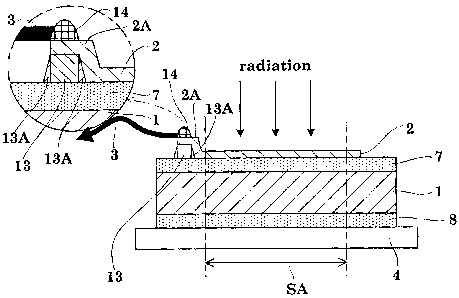
As shown in Figs. 2 and 3, the radiation detector in
the first embodiment includes a radiation sensitive
semiconductor I and a common electrode 2 for bias voltage
application. A lead wire 3 for supplying a bias voltage is
l0 connected to the surface of the common electrode 2. The
radiation sensitive semiconductor 1 gene~cates electric
charges upon incidence of radiation. The common electrode
2 for bias voltage application is formed two-dimensionally on
the front surface of the radiation sensitive semiconductor 1.
As shown in Fig. 4, the detector in the first embodiment
includes an active matrix substrate 4. Numerous collecting
electrodes 5 are formed on the surface of the active matrix
substrate 4, as shown in Fig. 5, i_n a two-dimensional matrix
arrangement set within a radiation detection effective area
SA. An electric circuit 6 is arranged on the surface of the
active matrix substrate 4 for storing and reading electric
charges collected by the respective collecting electrodes 5.
The radiation sensitive semiconductor 1 is laid on the sur-
face of the active matrix substrate 4 where the collecting
electrodes 5 are formed. A carrier selective intermediate
- 16-
CA 02480992 2004-09-09
layer '7 is formed between the radiation sensitive
semiconductor 1 and common electrode 2.. Another carrier
selective intermediate layer 8 is formed between the radia-
tion sensitive semiconductor 1 and collect;ing electrodes 5.
The storing and reading electric circuit 6 arranged on
the active matrix substrate 4 includes capacitors 6A, TFTs
(thin film field-effect transistors) 6B acting as switching
elements, gate lines 6a and data lines Fb. One capacitor 6A
and one TFT 6B are provided for each collecting electrode 5.
Around the storing and reading electric circuit 6 on the
active matrix substrate 4 are a gate driver 9,
charge-to-voltage converting amplifiers 10, a multiplexes 11
and an analog-to-digital converter 12 connected as external
devices. Some or all of the gate driver 9., charge-to-voltage
converting amplifiers 10, multiplexes 11 and ana-
log-to-digital converter 12 may be built into the active
matrix substrate 4, instead of being external devices.
In time of radiation detection by the detector in the
first embodiment, a bias voltage of several kilovolts to tens
of kilovolts outputted from a bias voltage source is applied to
the common electrode 2 via the lead wire 3. With the bias
voltage applied, the radiation sensitive semiconductor 1
generates electric charges upon incidence of the radiation to
be detected. The electric charges generated by the
semiconductor 1 are collected by the respective collecting
-17-
CA 02480992 2004-09-09
electrodes 5. More particularly, electric charges are
induced in the collecting electrodes 5 by rnovement to the
respective collecting electrodes 5. The electric charge
collected in each collecting electrode 5 is fetched by the stor-
y ing and reading electric circuit 6 on the active matrix sub-
strate 4 as a radiation detection signal for each collecting
electrode 5.
Specifically, as the gate driver 9 successively applies
read signals via gate lines 6a to the gates of the respective
l0 TFTs 6B, the data lines 6b connected to the sources of the
TFTs 6B receiving the read signals are successively switched
and connected to the multiplexer 11. With this switching
connection, the electric charges stored in the capacitors 6A
are transmitted from TFTs 6B through the data lines 6b,
15 amplified by the charge-to-voltage converting amplifiers 1~,
and outputted from the multiplexer 11 as radiation detection
signals for the respective collecting electrodes 5 to the ana-
log-to-digital converter 12 to be digitized therein.
Where, for example, the detector i_n the first embodi-
20 went is provided for a fluoroscopic apparatus, the radiation
detection signals outputted from the detector are transmit-
ted to an image processing circuit disposed at a subsequent
stage to create a two-dimensional fluoroscopic image or the
like .
25 That is, in the detector in the firsl~ embodiment, each
_ 18_
CA 02480992 2004-09-09
of the collecting electrodes 5 in the two-dimensional matrix
arrangement acts as an electrode corresponding to each pixel
in a radiographic image (pixel electrode). This detector is a
two-dimensional array type detector for providing radiation
detection signals for use in creating a radiographic image
according to a two-dimensional intensity distribution of the
radiation projected to the radiation detection effective area
SA.
The detector in the first embodiment may be
regarded as a detector having a two-dimension matrix
arrangement along longitudinal and transverse lattice lines
in the radiation detection effective area SA of radiation
detecting units (radiation detecting elements) in an equiva-
lent circuit shown in Fig. 6.
Each component of the detector in the first embodi-
ment will be described in greater detail hereinafter.
The detector in the first embodiment has an electri-
cally insulating buffer seat 13 disposed on the front surface
of the radiation sensitive semiconductor .L, outside the radia-
tion detection effective area SA. The common electrode 2
for bias voltage application is formed to cover a large part of
the buffer seat 13. The lead wire 3 for bias voltage supply
is connected to a portion located on the buffer seat 13 of the
surfaces of the common electrode 2. This is a salient
characteristic of the construction. That is, the carrier selec-
-19-
CA 02480992 2004-09-09
five intermediate layer 7 is provided in the first embodiment,
and the buffer seat 13 is formed to have a substantially
elliptical planar shape on the intermedialte layer 7. On the
other hand, part of the common electrode 2 continuously
extends out of the radiation detection effective area SA over
the buffer seat 13. A thin metal film (e.g. thin gold film) is
formed on that part to define a rectangular lead wire connec-
tion area 2A as an integral part of the common electrode 2.
The lead wire 3, such as a copper wire, is connected to the
surface of the lead wire connection area ~A by a conductive
paste (e.g. silver paste) 14. When the carrier selective
intermediate layer '7 is not provided, the common electrode 2
and buffer seat 13 will be formed directly on the surface of
the radiation sensitive semiconductor 1.
With the detector in the first embodiment, therefore,
when the lead wire 3 for bias voltage supply is connected to
the surface of the common electrode 2, the buffer seat 13
reduces the shock applied to the carrier selective intermedi-
ate layer 7 directly underneath and to the radiation sensi-
tive semiconductor 1 under the intermediate layer 7. This
is effective to prevent damage to the carrier selective
intermediate layer 7 and radiation sensitive semiconductor 1.
Since the buffer seat 13 which prevents damage to the
carrier selective intermediate layer '7 and. radiation sensitive
semiconductor 1 is disposed outside the radiation detection
-20-
CA 02480992 2004-09-09
effective area SA, the buffer seat 13 will never impair the
radiation detecting function.
Thus, the detector in the first embodiment can avoid
a lowering of performance resulting from the lead wire 3 for
bias voltage supply being connected to the common electrode
2 for applying a bias voltage to the radiation sensitive
semiconductor 1.
Further, with the detector in the first embodiment,
the buffer seat 13 prevents the conductive material in the
to conductive paste 14 electrically and mechanically connecting
the common electrode 2 and the lead wire 3 for bias voltage
supply, from moving (migrating) to the radiation sensitive
semiconductor 1. This is effective to avoid a deterioration of
electrical characteristics caused by migration of the conduc-
tive material in the conductive paste 14.
An appropriate height of the buffer seat 13 is in the
range of 0.2 to 2mm. This range will sufficiently reduce the
shock applied when the lead wire for bia~> voltage supply is
connected to the common electrode, and at the same time
assures a sufficient conduction reliability of the common
electrode in the portion of the buffer seat. A height of the
buffer seat 13 less than 0.2mm would provide an insufficient
thickness and render the seat 13 easily distortable, hence a
likelihood of failing to secure a sufficient buffer function.
Conversely, a height exceeding 2mm would readily cause a
-21-
CA 02480992 2004-09-09
poor conduction due to stepping of the common electrode 2,
thus tending to lower conduction reliability.
In the detector in the first embodiment, as shown in
Fig. 3, the buffer seat 13 includes a downwardly sloped seat
portion I3A formed around the entire side wall thereof and
having a thickness gradually decreasing outwardly away
from the seat 13. The c~mmon electrode 2 extends from the
radiation detection effective area SA to the top of the buffer
seat 13, following the surface of the sloped portion 13A.
to Thus, the common electrode 2 is shaped to climb the buffer
seat 13 gradually while extending along the surface of the
downwardly sloped seat portion I3A around the side wall of
the buffer seat 13. This construction can reliably avoid a
stepping of the common electrode 2 occurring in the region of
the buffer seat 13.
A stepping of the common electrode 2 would cause a
lowering of the bias voltage due to poor conduction. Then,
the same voltage applied to the lead wire connection area 2A
would not be applied to the portion of the common electrode
2 in the radiation detection effective area SA. Tt is there-
fore necessary to prevent a stepping of the common electrode
2 in order to avoid a shortage of bias voltage.
The buffer seat 13, preferably, is formed of a hard
resin material curable to a high degree of hardness, such as
epoxy resin, polyurethane resin, acrylic resin or the like.
-22-
CA 02480992 2004-09-09
The buffer seat 13 formed of a hard resin material does not
easily contract, and has an excellent buffer function. Thus,
the buffer seat 13 can fully reduce the shock occurring when
the lead wire 3 for bias voltage supply is connected to the
common electrode 2.
The sloped seat portion 13A may be formed of the
same hard resin material as the buffer seat 13, or may be
formed of a soft polymeric material of silicone resin or
synthetic rubber base.
The radiation sensitive semiconductor 1, preferably,
is high purity amorphous selenium (a-Se), an amorphous
semiconductor of selenium or selenium compound doped
with an alkali metal such as Na, a halogen such as Cl, As or
Te, or a non-selenium base polycrystalline semiconductor
such as CdTe, CdZnTe, PbI2, HgI2 or TIBr. These materials
are desirable because of their excellent aptitude for large
area and large film thickness. These semiconductors usu-
ally have a Mohs hardness of 4 or less, and thus are soft and
vulnerable to scratch. However, the buffer seat 13 can
reduce the shock occurring when the lead wire 3 for bias
voltage supply is connected to the common electrode 2,
thereby protecting the radiation sensitive semiconductor 1
from damage. This facilitates forming the radiation sensi-
tive semiconductor 1 with increased area and thickness. In
particular, amorphous selenium with a resistivity of 10952 or
-23-
CA 02480992 2004-09-09
greater, preferably 1O11SZ or greater, has an outstanding
aptitude for large area and large film thickness. The radia-
tion sensitive semiconductor 1 usually has a film thickness
of 0.5 to l.5mm and an area of 20 to 50crn by 20cm to 50cm,
for example.
As shown in Fig. 5, the active matrix substrate 4 has,
formed on an insulating substrate such as a glass substrate,
the capacitors 6A and TFTs 6B for the storing and reading
electric circuit 6, and the gate lines 6a and data lines 6b in a
l0 crisscross pattern. Further, the collecting electrodes 5 are
formed on the surface in a two-dimensional matrix arrange-
ment. The carrier selective intermediate Layer 8, radiation
sensitive semiconductor l, carrier selective intermediate
layer 7 and common electrode 2 are laminated in the stated
order on the surface of the active matrix substrate 4 having
the collecting electrodes 5.
The detector in the first embodiment, with the
carrier selective intermediate layers 7 and 8, can reduce
dark current. The carrier selectivity here refers to a prop-
erty of being remarkably different in contribution to the
charge transfer action between electrons and holes which
are charge transfer media (carriers) in a semiconductor.
The semiconductor 1 and carrier selective intermedi-
ate layers 7 and 8 may be combined in one of the following
modes. Where a positive bias voltage is applied to the com-
°24°
CA 02480992 2004-09-09
mon electrode 2, the carrier selective intermediate layer 7 is
formed of a material having a greater contribution of elec-
trons than of holes. This prevents an infiltration of holes
from the common electrode 2 to reduce dark current. The
carrier selective intermediate layer 8 is formed of a material
having a greater contribution of holes than of electrons.
This prevents an infiltration of electrons from the collecting
electrodes 5 to reduce dark current.
Conversely; where a negative bias voltage is applied
l0 to the common electrode 2, the carrier selective intermediate
layer 7 is formed of a material having a greater contribution
of holes than of electrons. This prevents an infiltration of
electrons from the common electrode 2 to reduce dark
current. The carrier selective intermediate layer 8 is
formed of a material having a greater contribution of elec-
trons than of holes. This prevents an infiltration of holes
from the collecting electrodes 5 to reduce dark current.
It is not absolutely necessary to provide carrier selec-
tive intermediate layers for the detector according to this
2o invention. One or both of the intermediate layers 7 and 8
may be omitted.
An appropriate thickness of the carrier selective
intermediate layers '7 and 8 is in the range of 0.1 to 10~,m.
A thickness of the intermediate layers 7 and 8 less than
O.I~,m tends to be incapable of suppressing dark current
-25-
CA 02480992 2004-09-09
sufficiently. Conversely, a thickness exceeding 10~,m tends
to obstruct radiation detection, e.g. tends to Iower sensitiv-
ity.
A semiconductor used for the carrier selective
intermediate layers 7 and 8 may be a polycrystalline
semiconductor such as Sb2S~, ZnTe, Ce02, CdS, ZnSe or ZnS,
or an amorphous semiconductor of selenium or selenium
compound doped with an alkali metal such as Na, a halogen
such as Cl, As or Te. These materials axe desirable because
to of their excellent aptitude for an enlarged area. These
semiconductors are thin and vulnerable to scratch. How-
ever, the buffer seat 13 can reduce the shock occurring when
the lead wire 3 fox bias voltage supply is connected to the
common electrode 2, thereby protecting the intermediate
layers 7 and 8 from damage. This facilitates forming the
carrier selective intermediate layers 7 and 8 with an
enlarged area.
Among the semiconductors usable for the intermedi-
ate layers 7 and 8, those having a large contribution of elec-
trons are n-type semiconductors including polycrystalline
semiconductors such as Ce02, CdS, CdSe, ZnSe and ZnS,
and amorphous materials such as amorphous selenium
doped with an alkali metal, As or Te to reduce the contribu-
tion of holes.
Those having a large contribution of boles are p-type
-26-
CA 02480992 2004-09-09
semiconductors including polycrystalline semiconductors
such as ZnTe, and amorphous materials such as amorphous
selenium dopes with a halogen to reduce the contribution of
electrons.
s Further, Sb2S3, CdTe, CdZnTe, PbI2, HgI2, TlBr,
non-doped amorphous selenium or selenium compounds
include the type having a large contribution of electrons and
the type having a large contribution of holes. Either type
may be selected for use as long as film forming conditions
l0 are adjusted.
A modification of the first embodiment is shown in
Figs. 7 and 8. Fig. 7 is a plan view showing a principal
portion of a detector. Fig. 8 is a sectional view showing the
principal portion of the detector. What is different from the
15 construction shown in Figs. 2 and 3 is an addition of an over-
coat 17 formed of a hard resin material and covering the
buffer seat 13 and sloped seat portion 13A. The other
details are the same as in the first embodiment.
While, in Figs. 7 and 8, the overcoat 17 extends to the
2o vicinity of the radiation detection effective area SA, what is
necessary is to cover at least the buffer seat 13 and sloped
seat portion 13A. The hard resin material for forming the
overcoat 17 may be epoxy resin, polyurethane resin, acrylic
resin or the like, as noted hereinbefore in relation to the
25 sloped seat portion 13A. That is, where the sloped seat
-27-
CA 02480992 2004-09-09
portion 13A is formed of a hard resin material, the same
material may be used for forming the overcoat 17.
In this modification, the overcoat 17 fixes and
protects the connection of the lead wire 3 for bias voltage
supply. Even when an external force is applied such as
when the lead wire 3 for bias voltage supply is detached, no
force is applied to cause cracks in the common electrode 2 on
the buffer seat 13 and sloped seat portion 13A. Thus, a
steady bias voltage may be supplied.
l0 Second Embodiment
A radiation detector in a second embodiment will be
described with reference to the drawings. Fig. 9 is a
sectional view showing a principal portion of the radiation
detector in the second embodiment.
As shown in Fig. 9, the detector in the second
embodiment includes a collimator 15 disposed at the radia-
tion incidence side for preventing the radiation incident on
the radiation detection effective area SA from impinging on
edges of the common electrode 2 and the buffer seat 13.
2o Apart from the collimator 15, this detector is the same as the
detector in the first embodiment. The common features will
not be described again, but only the different aspect will be
described below.
With the detector in the second embodiment, electric
fields formed by application of the bias voltage concentrate
-2S-
CA 02480992 2004-09-09
on the edges of the common electrode 2 and the side walls of
the buffer seat 13. When the radiation impinges on the
edges of the common electrode 2 and the side walls of the
buffer seat 13, contingent strong currents could flow that
would cause a failure of the detector (in particular, destruc-
tion of TFTs 6B of the storing and reading electric circuit 6).
Thus, in the second embodiment, the collimator 15
has an opening 15A formed so that the radiation may exactly
enter the radiation detection effective area SA without
l0 impinging on the edges of the common electrode 2 and the
buffer seat 13. As a result, the detector in the second
embodiment prevents the radiation from impinging on the
edges of the common electrode 2 and the buffer seat 13.
This detector can prevent contingent strong currents that
would cause a failure of the detector, from being produced by
the radiation impinging on the edges of the common elec-
trode 2 and the side walls of the buffer seat 13 where electric
fields concentrate.
Third Embodiment
A radiation detector in a third embodiment will be
described with reference to the drawings. Fig. 10 is a plan
view showing a principal portion of the detector in the third
embodiment. Fig. 11 is a fragmentary sectional view show-
ing edges of a common electrode of the detector in the third
embodiment.
-29-
CA 02480992 2004-09-09
In the detector in the third embodiment, as shown in
Fig. 10, an edge of the common electrode 2 extends to the top
of the buffer seat 13, following the surface of the sloped seat
portion 13A. In locations other than the buffer seat 13, a
sloped portion 16 for the electrode formed of an electrically
insulating polymeric material extends along the edges of the
common electrode 2. The sloped portion 16 has a thickness
gradually increasing outwardly of the common electrode 2.
The edges of the common electrode 2 extend and mount on
the sloped portion 16. Apart from the sloped portion 16
extending along the edges of the common electrode 2 in loca-
tions other than the buffer seat 13 and the edge of the com-
mon electrode 2 extending to the top of the buffer seat 13,
this detector is the same as the detector in the first embodi-
ment. The common features will not described again, but
only the different aspect will be described below.
The sloped portion 16 for the electrode is formed, as
is the sloped seat portion 13A, of a hard resin material such
as epoxy resin, polyurethane resin, acrylic resin or the like,
or a soft polymeric material of silicone resin or synthetic
rubber base.
Thus, in the detector in the third embodiment, the
edges of the common electrode 2 extend over the electrically
insulating buffer seat 13 and the sloped portion 16 for the
electrode formed of an electrically insulating polymeric
-30-
CA 02480992 2004-09-09
material. This eases the electric field concentration on the
edges of the common electrode 2, thereby reliably preventing
contingent strong currents that would cause a failure of the
detector (in particular, destruction of TFTs 6~ for storing
and reading electric circuit 6), from being produced by the
radiation impinging on the edges of the common electrode 2
and the side walls of the buffer seat 13.
This invention is not limited to the above embodi-
ments, but may be modified as follows:
(1) The detectors in the first to third embodiments
are the two-dimensional array type. The radiation detec-
tors according to this invention may be the one-dimensional
array type having collecting electrodes formed in a
one-dimensional matrix array, or the non-array type having
a single electrode for outputting radiation detection signals.
(2) The detectors in the first to third embodiments
include the analog-to-digital converter 1.2 besides the gate
driver 9, charge-to-voltage converting amplifiers 10 and
multiplexer 11. The invention may provide modified detec-
2o torn having the same constructions as in the first to third
embodiments, except that certain or all of the gate driver 9,
charge-to-voltage converting amplifiers 10, multiplexer 11
and analog-to-digital converter 12 are omitted.
(3) The detectors in the first to third embodiments
have the common electrode 2 partly extending to cover the
-31-
CA 02480992 2004-09-09
buffer seat 13. The common electrode 2 may extend not
only where the buffer seat is located but also in other loca-
tions. For example, the common electrode 2 may extend
from the radiation detection effective area to locations all
around the circumference the common electrode 2 to an
extent flush with the lead wire connection area 2A.
(4) The second and third embodiments may include,
as in the modification of the first embodiment, an overcoat
formed of a hard resin material and covering at least the
buffer seat 13 and sloped seat portion 13A.
This invention may be embodied in other specific
forms without departing from the spirit or essential attrib-
utes thereof and, accordingly, reference should be made to
the appended claims, rather than to the foregoing speci.fica-
tion, as indicating the scope of the invention.
-32-