Note: Descriptions are shown in the official language in which they were submitted.
CA 02481619 2004-09-15
-1-
MICRO-OPTIC DEVICE AND
METHOD OF MANUFACTURING SAME
BACKGROUND ART
The present invention relates to a micro-optic device including a
mirror and a complicate structure fabricated by a deep dry etching technique
such as a micro-optic device which is capable of light path switching and
light
intensity adjustment utilizing a mirror, and to a method of manufacturing such
a device.
An optical switch has been proposed in which a technique such as a
semiconductor anisotropic dry etching is used to form elements including a
mirror, a hinge, an actuator and a light guide on a substrate and which has
the
function of switching a light path by insertion into and extraction from the
light guide of the mirror.
To give a specific example, the structure of an MEMS
(Micro-Electro-Mechanical System) optical switch disclosed in U.S. Patent
No. 6, 315, 462, issued November 13, 2001, is shown in Fig. 1.
Formed in a sheet-like substrate 111 are four fiber channels 112a to
112d in a crisscross configuration. One of four areas which is defined by the
fiber channels 112a and 112b represents a drive formation 111'. A slot 113
which forms an angle of 45° with each of the fiber channels 112a and
112b is
formed in the drive formation 111', and a movable rod 114 is disposed in the
slot 113.
At its one end, the movable rod 114 carries a mirror 115, which is
positioned at an area of intersection 116 between the fzber channels 112a to
112d. Support beams 117a and 117b have their one end connected to
opposites sides of the movable rod 114 intermediate the length thereof, and
these support beams 117a and 117b have their other end secured to fixed
CA 02481619 2004-09-15
-2-
supports 119a and 1 I9b, respectively, through leaf spring hinges 118a and
118b. In a similar manner, support beams 117c and 117d have their one end
connected to opposite sides of the movable rod 114 at the other end thereof.
These support beams 117c and 117d have their other end secured to the fixed
supports 119a and 119b, respectively, through leaf spring hinges 118c and
118d. In this manner, the movable rod 114 is supported to be movable in the
lengthwise direction. It is to be noted that the leaf springs 118a, 118b, 118c
and 118d are folded back upon themselves to increase the spring length.
The movable rod 114 is driven by a comb tooth type electrostatic
actuator. Specifically, movable comb tooth electrodes 121 a to 121 d are
fixedly mounted as arrays on the support beams 117a to 117d, respectively,
and mate with fixed comb tooth electrodes 122a to 122d, respectively, which
are fixedly mounted on the drive formation 111'. When a voltage is applied
across the movable comb tooth electrodes 121 a and 121 b and the fixed comb
tooth electrodes 122a and 122b, an electrostatic force of attraction is
developed to move the movable rod 1 I4 in a direction toward the center of the
area of intersection 116. On the other hand, when a voltage is applied across
the movable comb tooth electrodes 121 c and 121 d and the fixed comb tooth
electrodes 122c and I22d, an electrostatic force of attraction is developed to
move the movable rod 114 in a direction away from the center of the area of
intersection 116. By driving the movable rod 114 with the comb tooth type
electrostatic actuator, it is possible to insert the mirror 115 into or to
extract it
from the center of the area of intersection 116.
Optical fibers 123a to 123d are respectively disposed in the four
fiber channels 1 I2a to I 12d. When the mirror 115 is inserted into the center
of the area of intersection 1 I 6, light which is emitted from the optical
fiber
123a, for example, is reflected by the mirror 115 to impinge on the optical
CA 02481619 2004-09-15
-3-
fiber 123d, and light which is emitted from the optical fiber 123b is
reflected
by the mirror 115 to impinge on the optical fiber 123c. On the contrary,
when the mirror is extracted from the center of the area of intersection 116,
light emitted from the optical fiber 123a impinges on the optical fiber 123c,
and light emitted from the optical fiber 123b impinges on the optical fiber
123d. A switching of the light path takes place in this manner.
The micro-optic switch is manufactured by the manufacturing
method shown in Fig. 2. Specifically, as shown in Fig. 2A, an SOI (Silicon
On Insulator) substrate 130 of a three layer construction including a single
crystal silicon substrate 131, on which an insulating layer 132 formed by a
silicon oxide film is formed, and a single crystal silicon layer 133 is
disposed
on top of the insulating layer 132 is provided. A required mask 134 is
formed on the single crystal silicon layer 133 by patterning a layer of mask
material. Portions of the single crystal silicon layer 133 which are exposed
through the mask 134 are subject to a deep anisotropic reacticve ion etching
(DRIE: Deep Anisotropic Reactive Ion Etching) to remove the single crystal
silicon layer 133 until the insulating layer 132 becomes exposed, as
illustrated
in Fig. 2B.
A narrow width portion 135 of the single crystal silicon layer 133 as
viewed in Fig. 2B represents movable parts such as the movable rod 114, the
support beams 117a to 117d and leaf spring hinges 118a to 118d shown in Fig.
1 while a wide width portion 136 represents a structural body such as the
fixed supports 119a and 119b shown in Fig. 1 which are fixedly mounted.
Fig. 2 is an exemplary illustration of these parts.
Referring to Fig. 2B, a wet etching is applied to the exposed
insulating layer 132 until a portion of the insulating layer 132 which is
disposed beneath the narrow width portion 135 is removed by a side etching.
CA 02481619 2004-09-15
-4-
As a consequence, the narrow width portion 13 5 will be located above the
single crystal silicon substrate 131 through an air gap 137, as shown in Fig.
2C. Thus, the movable part which is formed by the narrow width portion
135 as the insulating layer 132 is removed is spaced from the single crystal
silicon substrate 131 and becomes movable. It should be understood that the
mirror 115 is fabricated during the etching treatment of the single crystal
silicon layer 133 together with the movable rod 114, the support beams 117a
to 117d and the movable comb tooth electrodes 121 a to 121 d. Subsequent to
the wet etching operation, reflective films are formed by evaporation on the
lateral wall surfaces of the mirror 11 S, thus completing the mirror 115.
In this manner, when the anisotropic reactive ion dry etching
process is utilized, a vertical etched sidewall can be formed without being
influenced by the crystalline orientation of the single crystal silicon
substrate
131, thus enabling a minute structure of a complicate configuration as shown
in Fig. 1 to be manufactured. While a deep etching can be achieved by a wet
etching which uses an etchant solution applied to the single crystal silicon
layer, it is to be noted that this wet etching exhibits an anisotropic
behaviour
with respect to the crystalline orientation of the silicon, and therefore it
is
difficult to manufacture an optical device for a micro-electromechanical
system having a complicate construction as illustrated by the optical switch
shown in Fig. 1. For this reason, a micro-optic device of this kind has been
manufactured utilizing a deep anisotropic dry etching which utilizes a
reactive
ion.
However, when a deep anisotropic reactive ion etching is applied to
the single crystal silicon substrate 131 so that a deep vertical etched
sidewall
surface can be obtained, there results an unevenness which is in excess of the
order of 100nm on the etched sidewall surface. If an etched sidewall surface
CA 02481619 2004-09-15
.5.
having such an unevenness is used as a mirror surface for the movable mirror
115, the mirror cannot have a favorable reflection response. According to a
technology disclosed in the patent literature: International Laid-Open Number
WO 01/01 1411, Internationally Laid Open February 15, 2001, prior to the
deep anisotropic reactive ion etching, sacrificial raised layer masks 134b are
formed close to and on the opposite side of a mask 134a on a portion 115a of
the single crystal silicon layer 133 where the mirror 115 is subsequently to
be
formed in a mariner completely separate from masks 134c which are
associated with wide width portions 136. When the deep anisotropic
l0 reactive ion etching takes place subsequently, sacrificial raised layers
138 are
formed on the opposite sides of the masked portion 115a in closely adjacent
and parallel relationship threrwith. As shown in Fig. 3B, the single crystal
silicon layer 133 is immersed into an etchant 139, whereby movable parts
inclusive of the mirror portion 115a are free to move relative to the single
crystal silicon substrate 131. At this time, the sacrificial raised layers 13
8
are removed without being connected to any fixing part. By choosing such a
technology, the both sidewall surfaces of the mirror portion 11 Sa can be made
to be more smooth surfaces as compared with the surfaces which are obtained
without forming the sacrificial raised surfaces 138, with an unevenness on the
order of 30 nm or less.
However, it will be noted that there are a number of closely spaced
parts such as individual comb teeth of the comb tooth electrodes 121 a to I21
d
and 122a to 122d and folded back portions of the leafed spring hinges 118a to
118d which are closely spaced from each other. In particular, the insulating
layer 132 has a thickness which is normally on the order of 3~,m at most, and
the air gap between these movable parts and the single crystal silicon
substrate 131 is very narrow. If fragments of the sacrificial raised layers
138
CA 02481619 2004-09-15
-6-
which are separated from the substrate axe jammed into these narrow spaces,
the movable parts may become inoperable or there results adverse influences
upon the characteristic of the micro-optic device, leading to a degraded
yield.
It is known that the rough silicon surfaces on the opposite sidewall
surfaces of the mirror portion 11 Sa which are formed by the deep anisotropic
reactive ion dry etching may be thermally oxidized to form an oxide film of a
thickness which is large enough compared with the small unevenness of the
rough silicon surface, and the oxide film may be etched with a fluoric acid
(HF) to provide a mirror surface of a reduced roughness (see non-patent
literature : W.H. Juan and S.W. Pang, "Controlling sidewall smoothness for
micromachined Si mirrors and lenses", J. Vac. Sci. Technol. B 14(6),
Nov/Dec 1996, pp. 4080-4084).
However, with this technique, a time interval required to form an
oxide film which is sufficiently thick with respect to the minute unevenness
of
the surface by the thermal oxidation is as long as ten hours, for example,
requiring an increased manufacturing time for a micro-optic device, resulting
in a high cost of the optical device.
This problem is not limited to the micro-optic switch, but a similar
problem occurs when a micro-optic device including a mirror and a
complicate structure other than the mirror is subject to a gas reactive,
anisotropic dry etching to effect a deep etching reaction perpendicular to the
surface of the substrate.
SUMMARY OF THE INVENTION
It is an object of the present invention to provide a micro-optic
device including a mirror having a smooth mirror surface which can be
manufactured in a relatively reduced length of time and with a good yield, and
CA 02481619 2004-09-15
.7.
a method of manufacturing same.
In the micro-optic device according to the present invention, a
mirror has a minor surface which represents either ( 100) plane or ( I 11 )
plane
which is perpendicular to the sheet surface of a single crystal silicon
substrate.
The mirror surface as well as surfaces of structures other than the mirror are
sidewall surfaces perpendicular to the sheet surface of the substrate or
surfaces which are parallel to the sheet surface of the substrate.
According to the manufacturing method of the invention, an SOI
substrate is provided which includes an upper and a lower single crystal
silicon layer with an intermediate insulating layer, a mask layer is formed on
the top surface of the upper layer, and a mask is formed by patterning the
mask layer by photolithography so as to define a mirror forming surface
which is perpendicular to the sheet surface of the upper single crystal
substrate and which is aligned with either ( I 00) plane or ( 111 ) plane and
other
sidewall surfaces which are perpendicular to the sheet surface of the
substrate;
on the basis of the mask thus formed, the upper substrate which is
not masked is removed by the gas reactive anisotropic dry etching until the
intermediate insulating layer becomes exposed;
of the sidewall surfaces which are exposed by the dry etching
applied to the upper substrate, a surface which is aligned with either ( 100)
plane or ( I 11 ) plane is smoothened by a wet etchant solution which is
anisotropic with respect to silicon;
and of the smoothened surfaces which align with either ( 100) plane
or ( 111 ) plane, a surface which is to be formed as a mirror surface is
coated
with a metal having a high reflectivity.
According to the present invention, the mirror surface represents
either ( I 00) plane or ( 111 ) plane, but other vertical sidewall surfaces of
the
CA 02481619 2004-09-15
.8.
optical device structure are not restricted in this manner, allowing surfaces
which do not align with ( 100) plane or ( 111 ) plane or other
crystallographic
surface to remain. Accordingly, a deep etching by the anisotropic gas
reactive dry etching may be applied to the single crystal silicon substrate so
that the mirror surface is aligned with either ( 100) plane or ( 111 ) plane
to
form a minute structure having a complicate configuration. Subsequent to
the deep etching, an etching is performed using a solution which exhibits
anisotropy with respect to the crystalline orientation, whereby higher order
surfaces which are subject to a rapid etching rate are quickly etched and a
l0 mirror surface becomes a crystallographic surface which is aligned with
either
( 100) plane or ( 111 ) plane to provide a smooth mirror surface having an
unevenness on the order of l Onm or less while allowing the time interval for
the wet etching to be reduced. Because sacrificial raised layers are not
formed and are not required to be removed, there is no likelihood that the
response may be degraded, resulting in a better yield.
BRIEF DESCRIPTIONS OF THE DRAWINGS
Fig. 1 is a plan view of a conventional micro-optic switch;
Figs. 2A to 2C are partial cross sections schematically illustrating
several steps of a method of manufacturing the micro-optic switch shown in
Fig. 1;
Figs. 3A and 3B are schematic cross sections showing several steps
of another method of manufacturing a conventional micro-optic switch;
Fig. 4 is a plan view of an embodiment of the present invention;
Figs. SA, 5B and SC are cross sections of the optical device shown
in Fig. 4, as taken along the lines VA-VA, VB-VB and VC-VC, respectively;
Fig. 6 is a plan view, to an enlarged scale, illustrating a construction
CA 02481619 2004-09-15
-9-
of the optical device shown in Fig. 4 which is located in the vicinity of the
center of fiber channels which are arranged crisscross;
Fig. 7 is a plan view, to an enlarged scale, illustrating the
construction of a movable comb tooth electrode and a fixed comb tooth
electrode of the optical device shown in Fig. 4;
Figs. 8A and 8B are cross sections, to an enlarged scale, of an
exemplary leaf spring hinge used in the optical device shown in Fig. 4;
Fig. 9 is a plan view illustrating a condition that a mirror is
extracted from the center 1 c of fiber channels in the optical device shown in
Fig. 4;
Fig. 10 illustrate enlarged cross sections of various widths of leaf
spring hinges in superimposed relationship;
Fig. 11 graphically shows characteristic curves illustrating
exemplary relationships between the hinge width and the spring constant of
the leaf spring hinge;
Fig. 12 graphically shows characteristic curves illustrating
exemplary relationships between the hinge width error and the spring constant
of the leaf spring hinge;
Fig. 13A shows a condition that the leaf spring hinge may be held
attracted to a wall surface of a hinge recess by the action of a liquid which
remains during a drying step which follows the wet etching;
Fig. 13B shows a condition that the leaf spring hinge cannot be held
attracted to a wall surface of the hinge recess by the action of a liquid
which
remains during the drying step which follows the wet etching; and
Figs. 14A to 14D are cross sections taken along the line VA-VA
shown in Fig. 4, illustrating several steps of the method according to the
invention which is applied to manufacture a structure including a mirror of
the
CA 02481619 2004-09-15
'10_
optical device shown in Fig. 4.
MODE OF CARRYING OUT THE INVENTION
An embodiment of the present invention applied to the micro-optic
switch will now be described below with reference to the drawings. In the
description to follow, it should be noted that throughout the drawings,
corresponding parts are designated by like reference numbers without their
repeated description.
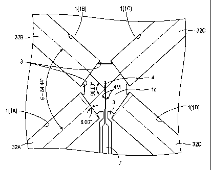
As shown in plan view in Fig. 4 and in cross sections in Fig. 5, an
l0 SOI three layer structure includes a sheet-like single crystal silicon
substrate
31 having a top surface 31 a in which fiber channels 1 are formed in a
crisscross configuration. Four fiber channels lA to 1D extend radially from
the center 1 c of an area of intersection between the crisscross fiber
channels 1,
and optical fibers 32A to 32D are inserted into the respective fiber channels.
As shown in Fig. 6, the width of fiber channels lA to 1D is defined so close
to
diameters of optical fibers 32A -32D that the fibers pressed into channels are
fixed within the channels, and the end face of each optical fiber is disposed
in
abutment against an abutment projection 3 which projects from the sidewall
near the center 1 c of the respective fiber channel 1 A to 1 D, whereby the
optical fibers 32A to 32D are positioned relative to the substrate 31. In this
example, the end face of each optical fiber 32A to 32D which is located
toward the center 1 c is beveled and abraded at an angle of 6°, for
example,
with respect to a plane which is perpendicular to the axis of the fiber to
function as a collimation fiber.
As shown in Fig. 4, one of four areas on the top surface 31 a of the
substrate 31 which are divided by the fiber channels 1 arranged crisscross
defines a drive formation 10, in which a rod channel 33 communicating with
CA 02481619 2004-09-15
-11-
the center I c is formed at an angle of 45° with respect to each of the
fiber
channels 1A and ID so as to bisect the angle therebetween. A movable rod 7
is disposed in the rod channel 33, and the movable rod 7 carries a mirror 4 at
its end disposed toward the center 1 c. Leaf spring hinges 6A to 6D are
connected to the movable rod 7 at two locations on each side to support the
movable rod 7 so as to be movable in the lengthwise direction thereof with a
movable path support 10a. In the example shown, each of the leaf spring
hinges 6A to 6D is slightly flexed in its major plane centrally, allowing the
hinge to assume two stable states which have reversed flexures.
A comb tooth type electrostatic actuator is provided between the
hinges 6A, 6C and the hinges 6B, 6D. Specifically, support arms Sa and Sb
have their one end secured to the opposite sides of the movable rod 7 and a
movable comb tooth electrode 5 is formed on the support arms Sa and Sb
toward the leaf spring hinges 6A and 6B and toward the leaf spring hinges 6C
and 6D. A first and a second fixed comb tooth electrode 8 and 9 are secured
to fixing parts 8a, 9a and 8b, 9b of the drive formation 10 which are disposed
toward the hinges 6C and 6D and toward the hinges 6A and 6B of the
movable comb tooth electrode 5. As shown to an enlarged scale in Fig. 7,
comb teeth on the movable comb tooth electrode 5 and the first and the
second fixed comb tooth electrode 8 and 9 are related such that the both comb
tooth electrodes 5 and 8 and 9 can mesh with each other. The minor 4, the
movable comb tooth electrode 5, the associated support arms Sa and Sb and
the movable rod 7 constitute together a movable part 1 l, which is retained by
the leaf spring hinges 6A to 6D to be movable on the movable part support
10a. As will be described later, the fixing parts 8a, 8b and 9a and 9b are
electrically insulated from the movable part support l0a which is connected to
the leaf spring hinges 6A to 6D.
CA 02481619 2004-09-15
-12-
In the present embodiment, the both lateral surfaces of the mirror 4
or the mirror surfaces 4M (Fig. 6) are perpendicular to the sheet surface of
the
sheet-like substrate 31 or the top surface 31 a and is aligned with the
crystallographic plane (100) of the single crystal silicon. An exposed
surface which is either parallel or orthogonal to the mirror surface 4M of the
micro-optic switch and which is perpendicular to the top surface 31 a
represents the crystallographic plane ( 100) of the silicon, but other
vertical
surfaces do not represent ( 100) plane. The top surface 31 a of the sheet-like
substrate 31 represents ( 100) plane.
As shown in Fig. 7, the leaf spring hinges 6A, 6B and 6C, 6D are
disposed within hinge recesses 14a and 14b, respectively, which axe formed in
the drive formation 10. Every surface which defines the outer profile of
structures other than the mirror 4, namely, the movable comb tooth electrode
5, the movable rod 7, the hinges 6A to 6D, and the first and the second fixed
comb tooth electrode 8 and 9 is either a sidewall surface perpendicular to the
sheet surface of the substrate (top surface 31 u) or a surface parallel to the
top
surface 31 u. In the initial condition which prevails immediately upon
manufacture of the optical device, it is preferred that wall surfaces of the
hinge recesses 14a and 14b which are located opposite to the sheet surface of
the leaf spring hinges 6A to 6D be parallel to oppositely located hinges 6A,
6B or 6C, 6D. Denoting a spacing between the leaf spring hinges 6A and 6B
and the fixing part 9a and 9b of the second fixed comb tooth electrode 9 and a
spacing between the same hinges and fixing parts disposed on the opposite
side from the f xing parts 9a and 9b by D l and D2, respectively, and denoting
a spacing between the leaf spring hinges 6C and 6D and the fixing part 8a and
8b of the first fixed comb tooth electrode 8 and a spacing between the same
leaf spring hinges and fixing parts disposed on the opposite side from the
CA 02481619 2004-09-15
-13-
fixing parts 8a and 8b by D3 and D4, respectively, it is desirable that these
spacings be equal to each other or D1=D2=D3=D4. In addition, as shown in
Figs. 8A and 8B, the cross-sectional configuration of the leaf spring hinges
6A
to 6D is preferably such that the opposite side surfaces are inclined
slightly,
for example, on the order of 81=O.S° with respect to a plane
perpendicular to
the sheet surface of the substrate 31u, and it is preferred that the width is
gradually reduced from the surface 6s (top surface 31u) toward the inner
surface. The cross-sectional configuration of the leaf spring hinges 6A to 6D
may be trapezoidal having a broader top side relative to the base as shown in
Fig. 8A or may be in the form of a wedge-shaped triangle as shown in Fig.
8B.
When the optical device has an initial configuration (which is
hereafter referred to as a first stable state) which is assumed immediately
after
it has been manufactured, the mirror 4 is located at the center 1 c, as shown
in
Fig. 4. At this time, light emitted from the optical fiber 32A is reflected by
the mirror 4 to impinge on the optical fiber 32B. Light emitted from the
optical fiber 32D is reflected and then impinges on the optical fiber 32C.
The movable comb tooth electrode S is electrically connected to the movable
part support 1 Oa through the movable rod 7 and the leaf spring hinges 6A to
6D, and when a voltage is applied to the first fixed comb tooth electrode 8
while the movable part support l0a and the second comb tooth electrode 9 are
connected to the ground, there occurs an electrostatic force of attraction
between the first fixed comb tooth electrode 8 and the movable comb tooth
electrode 5. If this force is greater than the force which tends to retain the
first stable state, the leaf spring hinges 6A to 6D reverse to the second
stable
state, and are maintained in this state by a self holding action if the
voltage
ceases to be applied. In this condition, the mirror 4 is retracted from the
CA 02481619 2004-09-15
-14-
center 1 c, and light emitted from the optical fibers 32A and 32B impinge on
the optical fibers 32C and 32D, respectively. When a voltage is applied to
the second fixed comb tooth electrode 9 while the movable part support l0a
and the first fixed tooth electrode 8 are connected to the ground, there
occurs
an electrostatic force of attraction between the second fixed comb tooth
electrode 9 and the movable comb tooth electrode 5, and if this force is
greater than the force which tends to retain the second stable state, the
hinges
revert to the first stable state again. To apply a voltage across the first or
the
second fixed comb tooth electrode 8 or 9 and the movable electrode 5,
bonding wires may be connected to the fixing parts 8a and 8b or 9a and 9b of
the first or the second fixed comb tooth electrode, and the voltage may be
applied across these bonding wires and the movable part support 10a.
Optical fibers 32A and 32B or 32C and 32D are given as an example of an
optical path formation in which extensions of optical paths intersect with
each
other on the mirror surface of the mirror 14.
It will be noted from Fig. 7 that the optical device is constructed so
that except for the mirror 4, the movable part 11 exhibits an axial symmetry
with respect to a center line parallel to the direction in which the mirror is
driven (or the center line of the movable rod 7) and that points A, B, C and D
where the movable rod 7 is supported by four leaf spring hinges 6A, 6B, 6C
and 6D (namely, where hinge reactions act) are disposed symmetrically with
respect to the connection between the movable comb tooth electrode 5 and the
movable rod 7 (or point S where the driving force acts). In addition, the
point S where the driving force acts is designed to be substantially in
coincidence with the center of gravity of the movable part 11. As a result of
such structural construction, if a driving force from the actuator contains a
vector component directed in a direction different from a direction in which
CA 02481619 2004-09-15
' 15'
the movable part is to be driven, the four leaf spring hinges 6A, 6B, 6C and
6D provide an equal reaction to the unnecessary vector component in the
driving force, thereby allowing an unintended movement of the movable part
11 in a direction other than a desired drive direction to be effectively
suppressed.
If an external disturbance such as impact is applied, two structural
features that 1 ) the four leaf spring hinges 6A, 6B, 6C and 6D are disposed
at
positions which are symmetrical with respect to the center of gravity of the
movable part 11 and that 2) the movable comb tooth electrode 5 which
represents a heavy structure is supported by the four leaf spring hinges 6A,
6B,
6C and 6D in an equal manner allow an unintended movement of the movable
part 11 to be effectively suppressed.
Since the opposite surfaces of the leaf spring hinges 6A to 6D axe
formed by slightly inclined tapered surfaces, reducing the width toward the
inside (or as further removed from the surface), the width of the hinges 6A to
6D on the surface which is required to provide a given spring constant can be
increased than when the cross section is rectangular, and this facilitates the
implementation of the photolithography applied when forming the mask while
reducing the manufacturing errors.
Specifically, the mechanical rigidity of the leaf spring hinges 6A to
6D is proportional to the third power of the thickness of the hinge, and
accordingly, the thickness of the hinges 6A to 6D has a great influence on the
dynamic response of the movable part 11. For this reason, in order to allow
an appropriate switching voltage to be obtained, it is necessary that the
thickness of the hinges 6A to 6D be machined to a very thin configuration on
the order of 1 ~.m, for example, requiring a very high manufacturing accuracy.
However, it is diffcult to achieve a satisfactory final finish configurational
CA 02481619 2004-09-15
-16-
accuracy in this region of sizes.
The cross-sectional configuration of the spring hinge 6 is assumed
to have a given value (0.5°, for example) for the angle of inclination
81 for the
tapered side surface, as shown in Fig. 10. Fig. 11 graphically shows a
relationship between the spring constant and the hinge width W 1 as measured
on the surface 6s, and Fig. 12 graphically shows a relationship between a
hinge width error and the spring constant for spring hinges 6 having a
trapezoidal or a triangular cross section and having various values for the
width W 1 or and for spring hinges having a rectangular cross section and
having the same width and the height as the spring hinges 6. In Fig. 11, the
abscissa represents the spring constant and the ordinate the hinge width W1,
and in Fig. 12, the abscissa represents a hinge width error and the ordinate
the
spring constant. In both Figures, a triangle mark d represents a hinge
having a trapezoidal or triangular cross section and a square mark D
represents a hinge having a rectangular cross section.
It is seen from Fig. 11 that for the same spring constant, a hinge
having a trapezoidal or triangular cross section can have a width W 1 which is
by 0.6N,m or more greater than a corresponding width of a hinge having a
rectangular cross section. It is also seen from Fig. 12 that as an error in
the
hinge width W 1 increases, the rate of a change in the spring constant is less
in
the hinge having a trapezoidal or triangular cross section than in the hinge
having a rectangular cross section, and accordingly, a greater design
allowance is permitted to the hinge having a trapezoidal or triangular cross
section for an equal error of the spring constant.
As mentioned above, it is preferred that the cross section of the leaf
springs 6A to 6D be in the form of an inverted trapezoid or an inverted
isosceles triangle with an angle of inclination of the lateral side on the
order
CA 02481619 2004-09-15
-17-
of 0.5°. However, the inclination of the lateral side of the leaf
springs 6A to
6D is achieved by the dry etching at the same time as the mirror surface is
formed. Light Loss caused by the inclination of the mirror surface 4M
depends on the diameter of a light beam. The light beam is throttled by a
collimation fiber formed at the inner end of each of the optical fibers 32A to
32D and assumes a minimum diameter (beam waist diameter) on the mirror
surface 4M. A light beam emitted from a single mode optical fiber has a
waist diameter on the order of 2.0 to 30.O~.m. Light loss in an optical switch
is attributable to a variety of factors, and a realistic permissible loss
which is
attributable to the inclination of the mirror surface 4M is on the order of
0.1 to
0.3 dB.
A calculation of light loss caused by the inclination of the mirror
surface for an optical wavelength of 1.55~.m and a horizontal angle of
incidence of 45° yields a maximum permissible loss of 0.3dB at the
minimum
beam waist diameter of 2.O~m for an angle of inclination A 1 equal to
5.25°.
On the other hand, an angle of inclination 81 which yields the minimum
permissible loss of 0.ldB at the maximum beam waist diameter of 30.O~xn is
equal to 0.20°. Consequently, a realistic angle of inclination A1 for
the
lateral side of the leaf springs 6A to 6D lies in a range from nearly
0.2° to 5.0°,
preferably nearly 0.5°.
During the drying step which follows the wet etching during the
manufacturing of the optical device, as the etchant becomes vaporized, the
etchant tends to be collected in a narrow region due to the action of the
surface tension of the etchant, and this is likely to cause an inconvenience
that
the movable part is held attracted to the fixing part by the surface tension
of
the liquid and remains fixed thereto under the influence of van der Waals
force when the drying step is completed. Such difficulty can be prevented
CA 02481619 2004-09-15
' 18'
by a technique in which the etching solution is replaced by a liquid which is
susceptible to sublimation under a reduced pressure, and the liquid is
solidified at a temperature on the order of 25°C, for example, to
promote the
sublimation of the resulting solid under a reduced pressure, by a
supercritical
drying process in which the etching solution is replaced by a liquefied carbon
dioxide (C02) and the drying step is continued in an environment of an
elevated temperature and high pressure which does not accompany a state
change from the liquid phase to the gas phase, or by a technique in which the
etching solution is simply replaced by another liquid having a reduced surface
tension for performing the drying step. Of these choices, it is simple to
perform the drying step using a liquid having a reduced surface tension, but
this has a drawback that the reliability is unwarranted.
To avoid this problem, it may be contemplated to increase the
mechanical rigidity of the leaf spring hinge to a degree which makes it to be
hardly attracted. However, the rigidity of the leaf spring hinges 6A-6B
cannot be increased in consideration of the relationship with the drive
voltage,
and the attraction is likely to occur. It is found that this is attributable
to the
reason mentioned below. Flexed leaf spring hinges 6A to 6D are used in
order to allow the movable part 11 to assume the first and the second stable
state. Accordingly, when the hinge recess 14 is made in the form of a
rectangle having a lengthwise direction which is substantially aligned with
the
lengthwise direction of the leaf spring hinge, the sheet surface of the Leaf
spring hinge 6 and the oppositely located wall surface of the hinge recess 14
may be widely spaced or closely spaced, giving rise to an offset in the timing
of vaporization of the liquid during the drying step. In the closely spaced
region, the vaporization of the liquid 1 S may be retarded and the surface
tension of the remaining liquid 15 (indicated by arrow 18) causes the hinge 6
CA 02481619 2004-09-15
-19-
to be attracted to the wall surface of the recess 14.
However, when the configuration of spaces on the opposite sides of
the leaf spring hinges 6A to 6D or the spacing between the sheet surface of
the hinge and the wall surface of the recess is made uniform as in the example
shown in Figs. 4 and 7, the amount of the liquid 15 which has undergone a
retarded vaporization becomes equal on the opposite sides of the hinge, as
shown in Fig. 13B, and accordingly, the magnitude of the surface tension of
the liquid 15 which remains on the opposite sides will be substantially equal
to each other, preventing the hinge from being held attracted. In this manner,
by providing an equal spacing between the hinge and the wall surfaces of the
recess which are located on the opposite sides of the hinge, a direct drying
step from a simple and convenient liquid can be reliably performed.
As will be apparent from the illustrations in Figs. 4 and SA to SC
and related descriptions, in the embodiment, surfaces constituting the mirror
14 and other structures or the movable part 11, the fiber channels 1 A to 1 D,
inclusive of the mirror surfaces are sidewall surfaces perpendicular to the
sheet surface of the substrate or surfaces parallel to the sheet surface of
the
substrate. In other words, the mirror and other structures have outer profiles
which axe formed by surfaces which are perpendicular to and which are
2o parallel to the sheet surface of the substrate.
An example of the method of manufacturing the optical device
shown in Figs. 4 to 7 will now be described with reference to Fig. 14, which
shows cross sections taken along the line VA-VA shown in Fig. 4 during
several steps.
As shown in Fig. 14A, a sheet-like substrate formed by a pair of
single crystal silicon layers 42 and 43 which are joined together through an
intermediate insulating layer 41 or so-called SOI substrate 31 is provided.
CA 02481619 2004-09-15
-20-
For example, the single crystal silicon layer 42 may comprise a single crystal
silicon substrate having a thickness of 350~,m, on which a silicon oxide film
41 is formed as the intermediate insulating layer, and the single crystal
silicon
layer 43 is formed as a single crystal silicon device layer 43 to complete the
substrate 31.
A layer of mask material 44 is formed on the substrate 31 or on top
of silicon device layer 43. The mask material may comprise a silicon oxide
film, for example.
Using the photolithography, for example, the Iayer of mask material
44 is patterned to form a mask 45 as shown in Fig. 14B on top of the mirror 4,
the hinges 6A-6D, the movable rod 7, the movable comb tooth electrode 5,
the first and the second fixed comb tooth electrode 8 and 9 and on top of the
substrate 31 excluding the fiber channels l, the rod channel 33 and space
(hinge recess 14) which does not influence upon the flexing operation of the
leaf spring hinges 6A-6D, or according to a pattern which defines the mirror
forming surface and side wall surfaces of structures other than the mirror
surfaces which are perpendicular to the sheet surface of the substrate, which
is
the pattern conf gured as shown in Fig. 4 in this embodiment. The layer of
mask material 44 is patterned so that the mirror surfaces of the mirror 4 are
aligned with (100) plane of the single crystal silicon. For this reason, the
SOI substrate 31 in which the top surface of the silicon device layer 43
represents ( 100) plane of the single crystal silicon is used.
Subsequently, by ICP-RIE (Inductively Coupled Plasma-Reactive
Ion Etching) dry etching, for example, the silicon device layer 43 is etched
in
a direction substantially perpendicular to the sheet surface of the sheet-like
substrate 31 using the mask 45 until the intermediate insulating layer 41
becomes exposed as shown in Fig. 14C. This forms the fiber channels 1, the
CA 02481619 2004-09-15
-21-
rod channel 33, the hinge recesses 14 and the comb teeth of the comb tooth
electrodes.
After the surface of the silicon device layer 43 including the side
walls which are formed by this etching operation is cleansed, it is immersed
in
a solution which exhibits an anisotropy of the etching rate with respect to
the
crystallographic orientation of the silicon and which has a reduced etching
rate at room temperature, which may be on the order of 0.03 ~,m/min, for
example, as exemplified by 8mol/liter (81~ solution of potassium hydroxide
(KOH) for an interval on the order of ten minuets at room temperature, thus
applying a slight degree of wet etching to the sidewalk which are formed by
the dry etching of the silicon device layer 43. An etchant solution for this
purpose may also comprise an aqueous solution of
ethylendiamine-pyrocatechol (EDP) or an aqueous solution of
tetramethylammonium hydroxide (TMAH), and it is preferred that a solution
having an etching rate on the order of 0.1 ~,m/min at room temperature be
used.
Subsequently, the substrate is immersed in a selective etchant
solution for the intermediate insulating layer 41 which may comprise a 50%
solution of fluoric acid (HF) (or a mixed solution of hydrofluoric acid and
ammonium fluoride) to etch the exposed intermediate insulating layer 41.
An etching time interval is chosen so that the intermediate insulating layer
41
is completely removed in regions corresponding to the movable part 11 such
as the mirror 4, the movable comb tooth electrode 5, the hinges 6A to 6D and
the movable rod 7, but the intermediate insulating layer 41 is only marginally
and slightly removed in regions corresponding to portions of the first and the
second fixed comb tooth electrodes 8 and 9 except for the comb teeth which
should remain fixed to the substrate 31. More specifically, the intermediate
CA 02481619 2004-09-15
-22-
insulating layer 41 located between the silicon device layer 43 and the single
crystal silicon substrate 42 is completely removed in narrow areas such as the
mirror 4, the movable comb tooth electrode 5, the hinges 6A to 6D, the
movable rod 7 and the comb teeth portions of the comb tooth electrodes 8 and
9, but the intermediate insulating layer 41 located between the silicon device
layer 43 and the single crystal silicon substrate 42 is only marginally
removed
in wider areas such as the fixing parts 8a, 8b, 9a and 9b, the movable part
support 10a.
As a result of this etching operation, the movable part 11 is
supported on the substrate 31 in a movable manner by the leaf spring hinges
6A to 6D, and the first fixed comb tooth electrode 48 and its associated
fixing
parts 8a and 8b, the second fixed comb tooth electrode 9 and its associated
fixing parts 9a and 9b and the movable part support l0a are electrically
insulated from each other. In addition, in this example, during this etching
operation, the mask 45 is simultaneously removed because the same material
is used for the intermediate insulating layer 41 and the layer of mask
material
44.
The cross sections taken along the lines VA-VA, VB-VB and
VC-VC after this etching operation appear as shown in Figs. SA , SB and SC
where corresponding parts to those shown in Figs. 4 and 14 are designated by
like reference characters.
The anisotropic wet etching which takes place for a limited time
interval with respect to the etched side walls of the silicon device layer 43
may follow the etching of the intermediate insulating layer 41 or the etching
which makes the movable part to be movable.
It should be noted that the both of these etching operations represent
a wet etching, and may take place in succession while changing the etching
CA 02481619 2004-09-15
-23-
solution without interposing a drying step between the both etching
operations.
After the deep, anisotropic dry etching has been applied to the
silicon device layer 43, the etched sidewall surfaces are rough surfaces which
can be regarded as an assembly of projections directed in random directions
which do not depend on the crystallographic orientation of the silicon (higher
order surface orientations). However, when an etching using an etchant
solution such as potassium hydroxide which exhibits an anisotropy of etching
rate with respect to the crystallographic orientation of the silicon is
applied,
higher order surfaces which are subject to a rapid etching rate are quickly
etched. Since the both surfaces of the mirror 4 represent ( 100) plane of the
silicon crystal, the anisotropic etching which depends on the
crystalllographic
orientation converts the mirror surfaces into smooth surfaces having an
unevenness in the direction of ( 100) plane of the silicon crystal on the
order of
1 Onm or less. The smoothed both surfaces of the mirror 4 are coated with a
metal having a high reflectivity such as Au/Pt/Ti multilayer film as by
sputtering, thus forming the mirror body.
The anisotropic wet etching applied to a single crystal silicon
normally takes place by using KOH solution at a temperature on the order of
70°C. In this instance, the etching rate will be on the order of 1
~.m/min,
which is by two orders of magnitude greater than the reduced etching rate
mentioned above, and when applied to the movable mirror 4 having a
thickness of 2N.m, the etching time will be very short, and unless the etching
time is precisely controlled, the minor portion will be dissolved, making the
control of the etching operation very difficult. However, this wet etching
can take place very easily in accordance with the invention because it takes
place at a reduced etching rate. While an etching rate on the order of
CA 02481619 2004-09-15
-24-
0.01 p,m/min at room temperature is preferred, but it is not limited to such
value. Since this choice is made because the etching rate on the order of
1.O~,m/min makes the etching control practically difficult, an etching rate
which enables easy etching control may be chosen to be 0.05 wm/min at room
temperature, for example, when a rapid etching is desired, but which may be
on the order of 0.1 to 0.2~m/min depending on the circumstance. If the
etching rate is too low, it takes a longer wet etching time, which is not
suitable
for industrial purpose. Accordingly, an etching rate on the order of 0.001 to
O.OOSN.m/min at room temperature may be chosen as a slow etching operation
while avoiding a significant retardation in the productivity.
Forming the both surfaces of the leaf spring hinges 6A to 6D as
tapered surfaces can be achieved by an etching operation with adjusted
etching conditions such that the sidewalls are slightly angled with respect to
the perpendicular to the surface of the substrate to make the thickness of the
hinge (the width of the cross section) reduced from the surface toward the
intermediate insulating layer 41 during the deep dry etching operation. In
this instance, the mirror surface of the mirror 4 or the crystallographic
surface
( 100) will be slightly offset from the perpendicular relative to the surface
of
the substrate (sheet surface of the substrate) when strictly viwed, but if the
offset is on the order of 0.5°, an influence upon optical performance
is
minimal. Throughout the specification, the sidewall surfaces which are
formed by the deep anisotropic reactive ion dry etching are described to be
perpendicular to the surface of the substrate (the sheet surface of the
substrate) inclusive of such slight offset.
The anisotropic wet etching which is applied to the sidewall
surfaces formed by the deep dry etching can also be utilized in a fine
adjustment of the thickness of the leaf spring hinges 6A to 6D which has a
CA 02481619 2004-09-15
-25-
great influence upon the dynamic response of the movable part 11.
In the above description, (100) plane is utilized as a surface which
is subject to a slow etching rate, and (100) plane of the single crystal
silicon
has been chosen for the mirror surface of the minor. However, an SOI
substrate 31 having ( 110) plane as the top surface of the silicon device
layer
43 may also be used so that the mirror has a mirror surface representing ( 111
)
plane and still the anisotropic wet etching may be used to provide a smooth
mirror surface. If one of these planes is to be chosen, ( 100) plane is
preferred.
In the above description, the present invention has been applied to a
mirror drive as a complicate structure other than the mirror 4, but the
application of the invention is not limited thereto, but the present invention
is
applicable to a micro-optic device in which a mirror and structures other than
the mirror are formed by the deep anisotropic dry etching in which the mirror
surface represents ( 100) plane or ( 111 ) plane of the single crystal silicon
and
is perpendicular to the sheet surface of the substrate and in which surfaces
which forms the mirror and structures other than the mirror are defined by
sidewall surfaces perpendicular to the sheet surface of the substrate or by
surfaces parallel to the sheet surface of the substrate, thus including such
device in which the mirror is fixed or in which the structures do not include
a
movable part, inclusive of the following examples:
~As movable devices:
Vaxiable Optic Attenuator (VOA) ~ ~ ~ substantially identical in
construction to an optical switch, in which leaf spring hinges lack the
function
of a bistable operation, and instead of controlling the mirror in a binary
movement, the mirror is continuously displaced in accordance with a drive
voltage applied.
CA 02481619 2004-09-15
-26-
Resonator Type Variable Optical Filter ~ ~ ~ a pair of mirrors are
disposed in opposing relationship to form a resonator, and at least one of the
mirrors is made to be variable to change the spacing between the mirrors for
changing the transmission wavelength characteristic of the resonator.
~As static devices:
an optical module used for transmission and reception of signals
including a mirror, an optical fiber, a semiconductor laser element, a light
receiving element and a sheet-like optical filter element. Grooves and spot
facings for mounting these elements are formed by the deep anisotropic
reacting ion dry etching. A micro-optic device including a pressure
mechanism having pressure springs (such as pressure spring 2 shown in Fig.
5) for positioning optical fibers and sheet-like optical filter elements.